Simple, High Saturation Power, Quantum-limited, RF SQUID Array-based Josephson Parametric Amplifiers
Abstract
High-fidelity quantum non-demolition qubit measurement is critical to error correction and rapid qubit feedback in large-scale quantum computing. High-fidelity readout requires passing a short and strong pulse through the qubit’s readout resonator, which is then processed by a sufficiently high bandwidth, high saturation power, and quantum-limited amplifier. We have developed a design pipeline that combines time-domain simulation of the un-truncated device Hamiltonian, fabrication constraints, and maximization of saturation power. We have realized an amplifier based on a modified NIST tri-layer Nb fabrication suite which utilizes an array of 25 radio frequency Superconducting QUantum Interference Devices (rf SQUIDS) embedded within a low-Q resonator powered by a high-power voltage pump delivered via a diplexer on the signal port. We show that, despite the intensity of the pump, the device is quantum-efficient and capable of high-fidelity measurement limited by state transitions in the transmon. We present experimental data demonstrating up to dBm input saturation power with dB gain, up to MHz instantaneous bandwidth, and phase-preserving qubit measurements with quantum efficiency.
I Introduction
Superconducting quantum computers are rapidly scaling to thousands of physical qubits [1]; more, high-fidelity qubit readout is a requirement for both Noisy Intermediate Scale (NISQ) [2] and error-corrected operation of these machines. To avoid further inflation of machine size via the use of ancilla qubits for error correction and other algorithms involving mid-circuit measurements, we require the readout to be Quantum Non-Demolition (QND), which leaves the qubit in the state indicated by the measurement outcome [3]. Moreover, dispersive superconducting qubit readout is limited by as yet imperfectly understood non-QND effects for strong readout drives [4, 5, 6, 7], and so one cannot increase the power of the measurement indefinitely to increase measurement fidelity. Further, due to the qubit’s finite , one must measure for a time much smaller than in order to attain high fidelity. Finally, we need a faithfully linear amplifier to amplify the short, few-photon quantum signal to be unaffected by the added noise of standard 4K commercial amplifiers in the upper stage of the readout chain while adding the minimum amount of noise allowed by quantum mechanics [8, 9].
Generally, we require these high-fidelity, QND measurements for each element of a quantum computer. Frequency multiplexing is a natural solution, allowing many qubit readout resonators to be measured from a single feed line as long as their resonant frequencies are sufficiently spaced. However, this spacing has to be larger than a few linewidths of the resonators to avoid crosstalk, necessitating a large bandwidth [10, 11, 12, 13] of the first amplifier in the chain. The presence of many signals at the same time also requires that the first amplifier also be highly linear, both avoiding compression and excess intermodulation distortion [12, 13].
The Josephson Parametric Amplifier (JPA) is one type of first-stage amplifier that shows promise for its ease of manufacture. The JPA’s megahertz-scale bandwidth typically falls well short of Josephson Travelling Wave Parametric Amplifiers (JTWPAs). However, the difficulty of manufacturing the thousands of junctions required for JTWPAs, their intrinsic loss, and noise-rise near saturation [14], motivates the study of how we can improve the JPA to create a small, easy-to-fabricate, quantum-limited amplifier. The primary shortcoming of simple JPAs with a single junction or loop is that they have very limited saturation power, typically less than dBm [15, 10, 16, 11, 17]. Depending on the choice of qubit parameters, this power may not be enough to amplify more than one or two qubits without distortion from saturation effects within the amplifier [12]. Diluting the nonlinearity of single junction/loop devices using a chain of DC SQUIDs, rf SQUIDs, and SNAILs has been explored both theoretically and experimentally, yielding substantially higher saturation power [18, 17, 19, 12, 13].
In this work, we design, fabricate, and characterize an extremely quantum-efficient and high-saturation power amplifier using a simple, single-mode device. The key component of our design process is numerical simulations of the un-truncated device Hamiltonian to fully understand and optimize the device within the constraints of fabrication. The key tuning parameters that we optimized are the device quality factor/impedance and the rf SQUID shunting ratio. The resulting simple design consists of merely two capacitors and an rf SQUID array using 25 junctions. We experimentally realized this device in a modified NIST tri-layer process. We demonstrate input referred saturation powers averaging dBm (dBm) with dB of power gain with extremes approaching dBm input saturation power and MHz instantaneous bandwidth using only 25 junctions. Additionally, we show that our amplifiers have high quantum efficiency (62% referred to the plane of the qubit), allowing fidelity measurements that are only limited by the qubit’s ability to tolerate photons in the readout resonator, not the amplifier’s saturation power.
II Amplifier Circuit Design and Fabrication
In this section, we present the device simulation and design within the bounds of fabrication. We begin by discussing the shortcomings of previous simulation efforts that truncate the nonlinearity in the device Hamiltonian. Following this, we discuss why we choose rf SQUIDs as our nonlinear elements. We also elaborate on our simulation method, which does not require truncation, and optimize the design parameters within our circuit. Lastly, we translate these optimization results into circuit elements with an added impedance transformation to control device quality factor.
The problem with single-junction or single-loop JPA’s is that even if their bandwidth is broadened to amplify the readout signals of multiple resonators, they struggle to reach the input saturation powers required to simultaneously amplify multiple readout signals at the dB gain required to overwhelm the added noise at the next stage of amplification at 4K [10, 11]. Measurements of this effect are shown directly in [12] in readout on a superconducting processor. This problem of JPA’s lacking power handling can be traced to the current through and phase difference across the Josephson junction at large input signals, which other works have focused on in some other similar amplifier designs [18, 17, 19]. However, these past works depend crucially on expansions of the junction nonlinearity around a particular bias point to find an analytical expression to guide design. While helpful to guide the designer’s intuition at small signal strengths, truncations to the junction Hamiltonian have been shown to obfuscate the high signal power behavior of Josephson junction-based devices [20, 17, 19], sometimes requiring extensions up to seven or eight orders to capture the nonlinear behavior of the junctions near amplifier saturation [20]. Because one of our chief goals is to increase amplifier saturation power, we instead simulate the device at large signal powers by finding a periodic steady-state solution of the device’s classical equation of motion in the time domain. This method is not without its drawbacks. Notably, it is more computationally intensive than methods such as harmonic balance and does not give any analytical understanding of the design. However, crucially, time domain simulations also do not require any simplification or truncation of the sinusoidal nonlinearity of the junction, and so are a far more accurate guide for the design of high-saturation power amplifiers.
To guide our design, we start with the same strategy as other work with DC SQUIDs [18] and Superconducting Nonlinear Asymmetric Inductive eLements (SNAILs) [21, 17]. If the oscillating phase of the signal increases to nearly , higher-order nonlinearities in the sinusoidal potential of the junction begin to become comparable to the third-order nonlinearity required for gain and disrupt amplification. This has been shown previously in similar studies of the same type of behavior in Josephson ring modulators [22, 20] as well as Josephson bifurcation amplifiers [18]. It has also been shown with fourth-order Kerr nonlinearity in SNAIL parametric amplifiers [21, 17, 19, 23]. All of these devices utilize a nonlinear shunt across the junction, formed by Josephson junctions of equal or higher critical currents. For high-inductance versions of these loops, an array of JJs is desirable for producing rather linear arrays with small geometric size. However, for large critical currents/small inductances, such as we use in amplifiers, it becomes quite feasible and desirable to use the geometric inductance of a short superconducting lead as the shunt, which has the additional advantage of eliminating concerns about array modes of the shunt itself [24, 17].
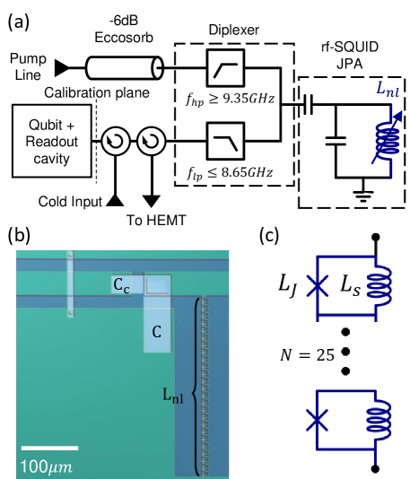
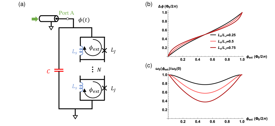
This device we refer to as an rf SQUID, though we acknowledge that is method of operation and biasing is rather different than the historical devices given this name [25]. We then carefully consider how best to optimize the circuit to maximize saturation power. To complement the dilution of the current through the junction by the linear inductive shunt, the phase is distributed by even division over an N-element series array similar to past work in Refs [18] and [17]. The full circuit with all external circuit elements is shown in Fig. 1(a). The result is similar to designs proposed in [26] but simpler, with only one array instead of two in parallel, albeit without an easy means of delivering flux on-chip over the entire array.
To simulate the device, we begin with the circuit diagram in Fig. A.1(a), with a single nonlinear mode formed from an array of rf SQUIDs of shunt inductance in parallel with a Josephson junction with inductance resonated by a capacitor , and coupled to the external environment of characteristic impedance around resonance. Assuming that the external magnetic fluxes through the rf SQUID,noted as , are the same, the equation of motion (EOM) can be expressed as
| (1) |
where the phase variable is defined by (see Fig. A.1a), is the external decay rate, and are two frequency constants.
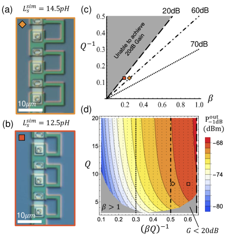
Using this simulation method, we find that controlling the dimensionless ratio of shunt to Josephson inductance , of each rf SQUID in the array and the quality factor of the resonator is critical to maximizing the saturation power of the rf SQUID while maintaining its ability to be pumped to produce gain. We find that the device should have approximately the same maximum achievable gain for constant , shown in Fig. 2(c) by different dashed/dash-dot/dotted lines through the design space. This is qualitatively similar to discussions about the product in SNAIL and JPC parametric amplfiiers, with having the same meaning as here, and being a ratio of SNAIL inductance to the total inductance of the mode. Much like in our rf SQUID case, there a higher , like , is "safer" in the sense that it ensures the amplifiers will achieve 20dB of gain [27, 17].
From our numerical calculations, we find that the design parameters Q and roughly outline a region where the amplifier will fail to achieve dB gain if the rf SQUID is shunted with too small an inductor or the quality factor is too low, as shown by the dashed line determined by a slope . For every point in the design space, we choose a flux bias point that maximizes the third-order nonlinearity in the rf-SQUID. However, we also find that variations in the saturation power with respect to flux bias are small in theory (see Fig. A.2(b)). Our principal result is that we also find that the maximum saturation powers of the device occur on the boundary outlined by the same dashed line through the design space in Fig. 2 (c) and (d), and can increase the saturation power in a 25-element long array by over dB compared to the lowest values. A higher inductive shunt produces a more nonlinear device with lower saturation power for a given Q, but more tunability in its inductance with respect to flux bias. For mode impedances that are controllably low (such that stray parallel capacitance and series inductances are small compared to the LC resonator that makes up the mode) at GHz, this sensitivity corresponds to requiring single micron-scale control over the exact dimensions of the inductive shunt of each rf SQUID in the array. Fig. 2(d) shows the design space of the amplifier assuming an rf-SQUID array in an embedding resonator with GHz.
Based on this understanding, we next scale the circuit by arraying N rf SQUIDs in series. A larger array lowers the nonlinearity by diluting the phase across each rf SQUID, raising the amplifier’s saturation power, but also making it harder to pump. Scaling the array by holding total array inductance constant and decreasing both the individual junction and shunt inductances as the array number increases would increase the saturation flux linearly. This yields quadratic saturation power scaling if one could maintain a constant mode impedance by scaling the junction critical current up and the shunt inductance down indefinitely. However, scaling the junction size up decreases its inductance, and since the designer has to maintain the same shunting ratio, the shunt inductance becomes difficult to control with optical lithography below about pH if the junction size is a few microns. Additionally, the junction side of the rf-SQUID has a stray inductance of a few pH, which can become comparable to the shunt as the scaling is increased. In combination, these effects put a lower bound on the achievable shunt inductance, and therefore an upper bound on the critical current of the junction. With this restriction in mind, we choose to use 25 rf SQUIDs that only require a comfortably low inductance pH shunt inductor and as the basic ingredient for our array.
Our fabricated devices, shown in Fig. 2(a) and (b), are fabricated in a modified niobium trilayer process at the National Institute for Standards and Technology’s Boulder Microfabrication Facility (layer specifications given in Appendix C.1), where the high yield and consistency of the junctions allows for excellent device yield in even very long junction arrays [28]. Even so, spatial nonuniformity in the flux biasing in the array (discussed in Appendix C.5 and C.3) presents an issue with verifying device parameters in the experiment. Accordingly, we discuss only the nominal designed values here, with the understanding that these parameters can reasonably vary by 10 percent or so in the real device. We use a shunting ratio of for device A, 0.21 for device B, and a junction inductance of .
In total, the rf SQUID array forms about pH of total effective inductance at zero DC-bias, and between to pH at the flux bias points which we expect to achieve dB gain. Provided this inductance is paired with a resonant capacitor that produces GHz we arrive at a capacitor value of to pF. If this mode were directly connected to a transmission line, we would expect a quality factor . However, as mentioned above, we have to alter the quality factor due to the increased inductance of the array compared to the single rf-SQUID. To increase the quality factor well into the region where we expect to achieve dB of gain (see Fig. 2(d)), we add a coupling capacitor pF to increase the effective environmental impedance on resonance to as seen by the JPA resonator, and increase the quality factor to approximately , with some added variance over bias flux because of the coupling capacitor’s frequency-dependent impedance. The effect of this variation with respect to flux and its consequences for the tunability of the amplifier’s gain is discussed in Appendix C.4.
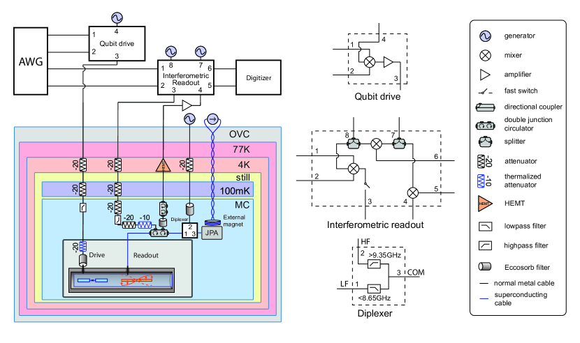
We measure the packaged JPA chip using a typical qubit readout amplification chain, with a few additions, such as eccosorb filters, a diplexer, and a modified pump line, that are detailed in Appendix C.2.
III Results
Cooled to mK in a dilution refrigerator, and powered with a strong pump at the 25-long rf-SQUID array shown in Fig. 2(a) and in the larger device in Fig. 1(b), is capable of generating a three-wave gain of more than dB over a range of bias points, shown in aggregate in Fig. 3(a) with more detail in Fig. C.5(b). To be sure we account for any loss introduced by the amplifier, we take the maximum return loss over all bias fluxes at each frequency as the baseline for gain. After using this pessimistic estimate to tune to dB of gain at each bias point, we measure input signal compression power up to a maximum of dBm, which is among the highest values reported in the literature for a Josephson junction-based resonant parametric amplifier, in good company with the extreme values of [17, 19, 23], and the average values in other rf-SQUID based devices [12, 13]. Notably, devices of this type achieve similar saturation powers even to JTWPAs that contain almost one hundred times more junctions [29].
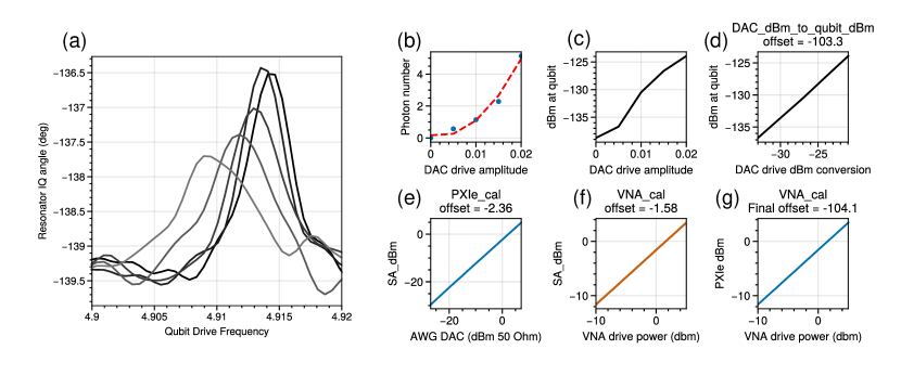
Power is calibrated at GHz by measuring resonator photon number-induced shifts of the qubit’s transition frequency () combined with separate measurements of the qubit-cavity dispersive shift, detailed in Appendix C.6 along the lines of [30].
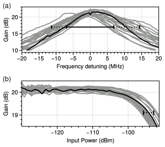
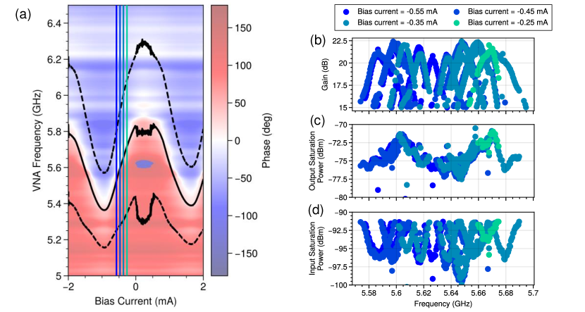
Average input saturation power values are dBm, with an average instantaneous bandwidth of MHz. As shown in Fig. 3(b) with more detail in Fig. C.5, the gain varies somewhat in profile with respect to pump detuning at any given bias point, which we attribute to ripples in the line impedance. Further, because the pessimistic baseline we have chosen for gain is not necessarily flat with respect to frequency and is combined from all bias points, some of the gain profiles are asymmetric with respect to . If we take a less pessimistic baseline, only normalizing to one flux bias point at a time, they appear symmetric as expected. However, some variation in the shape of the loss is expected with the device’s low quality factor because the device responds to changes in the external environment over its linewidth of approximately MHz, with variations over flux bias. This significantly impacts the pumped operation of the device, because the characteristic ripples in the external environment occur on the same MHz scale. Consequently, the gain profile should take on a modified profile depending on the local slope of the external environment at that particular signal frequency. In addition to the shapes shown, it is possible to see double-peaked gain profiles similar to [11]. We fall short of the expected gain-bandwidth product for many bias points partly because of this issue of variable port impedance. There is also significant uncertainty in the fit for the device linewidth due to the same impedance ripples, so it is possible the device linewidth may be lower than designed.
The input-referred saturation power of the amplifier depends slightly on bias settings and certain parameters that vary on the dB level in the external environment, such as the loss between the resonator cavity and the amplifier chip. Within these variations, the data shows reasonable agreement with the theoretically predicted value from periodic-steady-state analysis of the device equation of motion, shown in Fig. A.2. The high saturation power of the rf-SQUID JPA that we demonstrate is critical for enabling many-qubit readout experiments. However, despite the diplexer’s rejection, the pump power (approximately -25 to -30dBm, based on room temperature loss calibrations) required and the lack of attenuation on the pump line might raise concerns over the thermal photon occupation in the readout resonator and the corresponding limits imposed on from thermal photons in the readout resonator dephasing the qubit.
| Amplifier State | () | () | () |
|---|---|---|---|
| Replaced with short | 81 | 8 | 20 |
| Off | 90 | 13 | 26 |
| Detuned -500MHz | 93 | 11 | 18 |
| On (25dB Gain) | 91 | 6.4 | 9.1 |
To address this concern, we measure qubit coherence with varying pump conditions in Table 1. We speculate that the presence of the high-power pump line is not meaningfully contributing to decoherence at the level, otherwise we would have expected that the qubit coherence would have improved in the absence of the amplifier and diplexer combination in row 1. It must be noted, however, that this measurement was taken on a different cooldown than the others, and qubits can have significant variation in coherence from cooldown to cooldown. Avoiding dephasing is crucial to the design of high-saturation JPAs, allowing the pump inefficiency to be tolerable in terms of qubit coherence albeit inconvenient for fridge design, requiring specially engineered lines with lower attenuation in order to deliver high power pumps without excess heating. However, we observe the time of the qubit dip distinctly when the amplifier is turned on, indicating that the amplifier introduces an extra source of dephasing onto the qubit from the gain alone. This effect is often observed in high-efficiency measurement setups [31, 32], and can be the result of insufficient isolation between the JPA and the readout resonator. To combat this, one can use additional circulators for isolation at the cost of a modest loss in quantum efficiency [13].
In order to calibrate the efficiency of the amplification chain from the plane of the qubit, we can measure the back-action that the amplifier introduces on the qubit. We turn the amplifier on at dB gain, prepare the qubit in the state, and apply two measurements in sequence according to the pulse diagram in Fig. 4(a) [33].
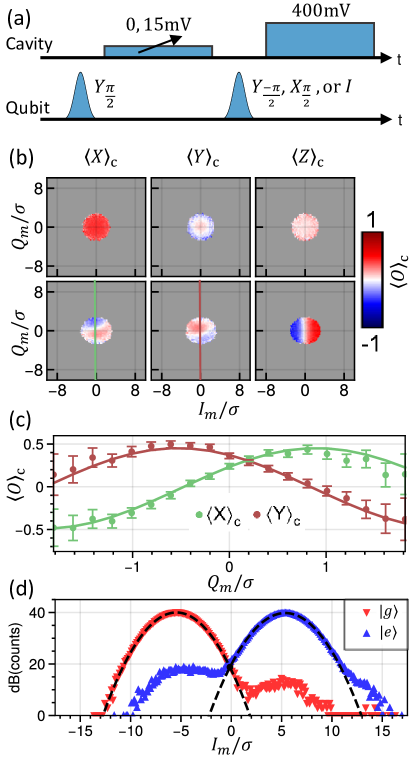
The back-action of the weak measurement results in a sinusoidal pattern in the and expectation values in Fig. 4(b), with linecuts in Fig. 4(c) with respect to the result of the weak measurement. This sinusoidal pattern has frequency set by the measurement strength , but the amplitude is diminished by an exponential dependent on the measurement strength scaled by the quantum efficiency [33]. Because measurement strength is independently set by the distance between coherent pointer states in the IQ plane, we can fit these oscillations to extract the quantum efficiency. Because the IQ values are dependent on the entire readout chain, the quantum efficiency that results from the fit represents the efficiency of the entire readout chain, including losses and added noise from the higher-stage amplifiers at and room temperature. Therefore, it acts as a safe lower bound for the efficiency of the rf-SQUID JPA itself.
With this method, we find a measurement efficiency of on a scale of 0 to 1, without compensating for state preparation and measurement error. This is among the highest reported quantum efficiency values for phase-preserving amplifiers [34, 35, 12, 13], however still not as efficient as phase-sensitive nonreciprocal amplification [32], serving as motivation to pursue integrating amplification closer to the readout resonator itself. The high quantum efficiency of our device also serves as evidence that the high-power nature of the rf-SQUID JPA does not detract from its efficiency.
The projective state readout fidelity of the qubit suffered from a below optimal , where MHz is the change in readout resonator frequency between and states of the qubit and MHz is the readout resonator linewidth. So, despite high readout efficiencies, the decay of the qubit limits the phase-preserving readout fidelity to with a pulse length, as shown in Fig. 4(d). As a result, despite the high saturation power of the amplifier, we were unable to increase the readout power and shorten the pulse time due to readout-induced state transitions in the qubit. For examples of high-power readout histograms, see Fig. C.6.
Higher state transitions in qubit-cavity systems at high cavity occupation is an oft-observed phenomenon [4, 6, 5, 7]. However, it is not entirely without counter. One can design linear filters that take into account quantum noise and decay [36, 37]. Even with such filters the behavior of transmon qubits at very high readout resonator occupations is generally detrimental to readout performance, and remains a barrier to fast, high-fidelity, QND measurement. Future work to improve the state of the art, including the study of transmon dynamics at high power, will hopefully be enabled by a robust measurement chain that can easily tolerate the measurement powers that drive transmons into behavior resembling chaos [7].
IV Conclusion
To conclude, we have experimentally demonstrated the effectiveness of periodic steady-state simulations for capturing JPA dynamics. Using these tools we have successfully designed, built, and fabricated a high saturation power JPA built on rf-SQUID arrays with enough power handling capability for hundreds of channels of simultaneous measurements, albeit without the bandwidth to demonstrate this capability. Additionally, we have shown that despite the device’s need for a high-power pump, it does not reduce qubit coherence beyond what is expected for a single stage of isolation, which can be further circumvented by pulsing the amplifier. In addition, the device maintains quantum efficiency on par with some of the best examples of phase-preserving amplification in the literature. We show high fidelity measurement limited primarily by readout-activated state transitions in the qubit at high powers, rather than any property of amplifier itself. The non-QND nature of strong measurement tones in circuit QED remains an open problem for the field which motivates the pursuit of optimal filtering [37] and a greater understanding of the limitations of the limits of dispersive readout in circuit QED [5, 7, 38].
Future work includes engineering a robust matching network to broaden the gain response of this amplifier with techniques similar to [39, 13]. However, we note that while these techniques outline an elegant solution that traces roots back to filter synthesis, the technique must also be unified with the saturation power calculations demonstrated in this work which account for the full nonlinearity of the Josephson junction to further assist the designer in anticipating saturation effects. More, we should implement a dedicated pump coupling port that can avoid the inefficiency of the coupling capacitor as a means of delivering the AC driving phase to the junction at the pump frequency. This could effectively integrate the external diplexer on-chip, which can be feasibly implemented with the existing fabrication process, which will greatly simplify the external circuitry required to operate the amplifier and conceivably reduce the loss between the amplifier and qubit to further increase the efficiency of measurements. Additional research is also being done on how to increase the amplifier’s power-added efficiency once the pump reaches the resonator node [40]. In all, we demonstrate a simple and highly linear amplifier that can serve as a stepping stone for these innovations and as a workhorse in near-term quantum information experiments, including the study of the QNDnesss of strong qubit readout.
Acknowledgements
We are grateful to the Peterson Institute for Nanoscience and Engineering for support in the fabrication of the qubit used for measurement. We thank Chao Zhou and Pinlei Lu for their work and helpful guidance on the control and measurement software. This manuscript is based upon work supported in part by the U.S. Army Research Office under Grant No. W911NF-15-1-0397 and the National Institute of Standards & Technology (NIST) Quantum Information Program. Boris Mesits was supported by the NSF GRFP. This material is based upon work supported in part by the U.S. Department of Energy, Office of Science, National Quantum Information Science Research Centers, Co-design Center for Quantum Advantage (C2QA) under contract number DE-SC0012704, (Basic Energy Sciences, PNNL FWP 76274). The Pacific Northwest National Laboratory is operated by Battelle for the U.S. Department of Energy under Contract DE-AC05-76RL01830. This is a contribution of the National Institute of Standards and Technology, not subject to U.S. copyright. Any identification of commercial equipment, instruments, or materials in this paper is to foster understanding; it does not imply neither the recommendation or endorsement by the National Institute of Standards and Technology, nor does it imply that the materials or equipment identified are necessarily the best available for the purpose.
References
- IBM [2024] IBM quantum roadmap to build quantum-centric supercomputers | IBM research blog (2024), https://research.ibm.com/blog/ibm-quantum-roadmap-2025.
- Preskill [2018] J. Preskill, Quantum Computing in the NISQ era and beyond, Quantum 2, 79 (2018).
- Nielsen and Chuang [2010] M. A. Nielsen and I. L. Chuang, Quantum Computation and Quantum Information: 10th Anniversary Edition (Cambridge University Press, 2010).
- Sank et al. [2016] D. Sank, Z. Chen, M. Khezri, J. Kelly, R. Barends, B. Campbell, Y. Chen, B. Chiaro, A. Dunsworth, A. Fowler, E. Jeffrey, E. Lucero, A. Megrant, J. Mutus, M. Neeley, C. Neill, P. J. O’Malley, C. Quintana, P. Roushan, A. Vainsencher, T. White, J. Wenner, A. N. Korotkov, and J. M. Martinis, Measurement-induced state transitions in a superconducting qubit: Beyond the rotating wave approximation, Physical Review Letters 117, 190503 (2016).
- Shillito et al. [2022] R. Shillito, A. Petrescu, J. Cohen, J. Beall, M. Hauru, M. Ganahl, A. G. Lewis, G. Vidal, and A. Blais, Dynamics of transmon ionization, Physical Review Applied 18, 034031 (2022).
- Khezri et al. [2023] M. Khezri, A. Opremcak, Z. Chen, K. C. Miao, M. McEwen, A. Bengtsson, T. White, O. Naaman, D. Sank, A. N. Korotkov, Y. Chen, and V. Smelyanskiy, Measurement-induced state transitions in a superconducting qubit: Within the rotating-wave approximation, Physical Review Applied 20, 054008 (2023).
- Cohen et al. [2023] J. Cohen, A. Petrescu, R. Shillito, and A. Blais, Reminiscence of classical chaos in driven transmons, PRX Quantum 4, 020312 (2023).
- Caves et al. [2012] C. M. Caves, J. Combes, Z. Jiang, and S. Pandey, Quantum limits on phase-preserving linear amplifiers, Physical Review A - Atomic, Molecular, and Optical Physics 86, 063802 (2012).
- Clerk et al. [2010] A. A. Clerk, M. H. Devoret, S. M. Girvin, F. Marquardt, and R. J. Schoelkopf, Introduction to quantum noise, measurement, and amplification, Reviews of Modern Physics 82, 1155 (2010).
- Mutus et al. [2014] J. Y. Mutus, T. C. White, R. Barends, Y. Chen, Z. Chen, B. Chiaro, A. Dunsworth, E. Jeffrey, J. Kelly, A. Megrant, C. Neill, P. J. O’Malley, P. Roushan, D. Sank, A. Vainsencher, J. Wenner, K. M. Sundqvist, A. N. Cleland, and J. M. Martinis, Strong environmental coupling in a Josephson parametric amplifier, Applied Physics Letters 104, 263513 (2014).
- Roy et al. [2015] T. Roy, S. Kundu, M. Chand, A. M. Vadiraj, A. Ranadive, N. Nehra, M. P. Patankar, J. Aumentado, A. A. Clerk, and R. Vijay, Broadband parametric amplification with impedance engineering: Beyond the gain-bandwidth product, Applied Physics Letters 107, 262601 (2015).
- White et al. [2023] T. White, A. Opremcak, G. Sterling, A. Korotkov, D. Sank, R. Acharya, M. Ansmann, F. Arute, K. Arya, J. C. Bardin, A. Bengtsson, A. Bourassa, J. Bovaird, L. Brill, B. B. Buckley, D. A. Buell, T. Burger, B. Burkett, N. Bushnell, Z. Chen, B. Chiaro, J. Cogan, R. Collins, A. L. Crook, B. Curtin, S. Demura, A. Dunsworth, C. Erickson, R. Fatemi, L. F. Burgos, E. Forati, B. Foxen, W. Giang, M. Giustina, A. G. Dau, M. C. Hamilton, S. D. Harrington, J. Hilton, M. Hoffmann, S. Hong, T. Huang, A. Huff, J. Iveland, E. Jeffrey, M. Kieferová, S. Kim, P. V. Klimov, F. Kostritsa, J. M. Kreikebaum, D. Landhuis, P. Laptev, L. Laws, K. Lee, B. J. Lester, A. Lill, W. Liu, A. Locharla, E. Lucero, T. McCourt, M. McEwen, X. Mi, K. C. Miao, S. Montazeri, A. Morvan, M. Neeley, C. Neill, A. Nersisyan, J. H. Ng, A. Nguyen, M. Nguyen, R. Potter, C. Quintana, P. Roushan, K. Sankaragomathi, K. J. Satzinger, C. Schuster, M. J. Shearn, A. Shorter, V. Shvarts, J. Skruzny, W. C. Smith, M. Szalay, A. Torres, B. W. Woo, Z. J. Yao, P. Yeh, J. Yoo, G. Young, N. Zhu, N. Zobrist, Y. Chen, A. Megrant, J. Kelly, and O. Naaman, Readout of a quantum processor with high dynamic range Josephson parametric amplifiers, Applied Physics Letters 122, 14001 (2023).
- Kaufman et al. [2023] R. Kaufman, T. White, M. I. Dykman, A. Iorio, G. Stirling, S. Hong, A. Opremcak, A. Bengtsson, L. Faoro, J. C. Bardin, T. Burger, R. Gasca, and O. Naaman, Josephson parametric amplifier with chebyshev gain profile and high saturation, Physical Review Applied 20, 054058 (2023).
- Remm et al. [2023] A. Remm, S. Krinner, N. Lacroix, C. Hellings, F. Swiadek, G. J. Norris, C. Eichler, and A. Wallraff, Intermodulation distortion in a Josephson traveling-wave parametric amplifier, Physical Review Applied 20, 034027 (2023).
- Yamamoto et al. [2008] T. Yamamoto, K. Inomata, M. Watanabe, K. Matsuba, T. Miyazaki, W. D. Oliver, Y. Nakamura, and J. S. Tsai, Flux-driven Josephson parametric amplifier, Applied Physics Letters 93, 42510 (2008).
- Zhou et al. [2014] X. Zhou, V. Schmitt, P. Bertet, D. Vion, W. Wustmann, V. Shumeiko, and D. Esteve, High-gain weakly nonlinear flux-modulated Josephson parametric amplifier using a squid array, Physical Review B - Condensed Matter and Materials Physics 89, 214517 (2014).
- Frattini et al. [2018] N. E. Frattini, V. V. Sivak, A. Lingenfelter, S. Shankar, and M. H. Devoret, Optimizing the nonlinearity and dissipation of a SNAIL parametric amplifier for dynamic range, Physical Review Applied 10, 054020 (2018).
- Kochetov and Fedorov [2015] B. A. Kochetov and A. Fedorov, Higher-order nonlinear effects in a Josephson parametric amplifier, Physical Review B - Condensed Matter and Materials Physics 92, 224304 (2015).
- Sivak et al. [2019] V. V. Sivak, N. E. Frattini, V. R. Joshi, A. Lingenfelter, S. Shankar, and M. H. Devoret, Kerr-free three-wave mixing in superconducting quantum circuits, Physical Review Applied 11, 054060 (2019).
- Liu et al. [2020] C. Liu, T. C. Chien, M. Hatridge, and D. Pekker, Optimizing Josephson-ring-modulator-based Josephson parametric amplifiers via full Hamiltonian control, Physical Review A 101, 042323 (2020).
- Frattini et al. [2017] N. E. Frattini, U. Vool, S. Shankar, A. Narla, K. M. Sliwa, and M. H. Devoret, 3-wave mixing Josephson dipole element, Applied Physics Letters 110, 222603 (2017).
- Liu et al. [2017] G. Liu, T. C. Chien, X. Cao, O. Lanes, E. Alpern, D. Pekker, and M. Hatridge, Josephson parametric converter saturation and higher order effects, Applied Physics Letters 111, 20 (2017).
- Sivak et al. [2020] V. V. Sivak, S. Shankar, G. Liu, J. Aumentado, and M. H. Devoret, Josephson array-mode parametric amplifier, Physical Review Applied 10, 24014 (2020).
- Masluk et al. [2012] N. A. Masluk, I. M. Pop, A. Kamal, Z. K. Minev, and M. H. Devoret, Microwave characterization of josephson junction arrays: Implementing a low loss superinductance, Physical Review Letters 109, 137002 (2012).
- Clarke and Braginski [2005] J. Clarke and A. I. Braginski, The SQUID Handbook, Vol. 1 (Wiley Blackwell, 2005) pp. 1–395.
- Naaman et al. [2019] O. Naaman, D. G. Ferguson, A. Marakov, M. Khalil, W. F. Koehl, and R. J. Epstein, High saturation power Josephson parametric amplifier with ghz bandwidth, IEEE MTT-S International Microwave Symposium Digest 2019-June, 259 (2019).
- Bergeal et al. [2010] N. Bergeal, R. Vijay, V. E. Manucharyan, I. Siddiqi, R. J. Schoelkopf, S. M. Girvin, and M. H. Devoret, Analog information processing at the quantum limit with a josephson ring modulator, Nature Physics 2010 6:4 6, 296 (2010).
- Niemeyer et al. [1985] J. Niemeyer, L. Grimm, W. Meier, J. H. Hinken, and E. Vollmer, Stable josephson reference voltages between 0.1 and 1.3 v for high-precision voltage standards, Applied Physics Letters 47, 1222 (1985).
- Macklin et al. [2015] C. Macklin, K. O’Brien, D. Hover, M. E. Schwartz, V. Bolkhovsky, X. Zhang, W. D. Oliver, and I. Siddiqi, A nearâ€"quantum-limited Josephson traveling-wave parametric amplifier, Science 350, 307 (2015).
- Schuster [2007] D. I. Schuster, Circuit Quantum Electrodynamics, Ph.D. thesis, Applied Physics (2007).
- Lecocq et al. [2017] F. Lecocq, L. Ranzani, G. A. Peterson, K. Cicak, R. W. Simmonds, J. D. Teufel, and J. Aumentado, Nonreciprocal microwave signal processing with a field-programmable Josephson amplifier, Physical Review Applied 7, 024028 (2017).
- Lecocq et al. [2021] F. Lecocq, L. Ranzani, G. A. Peterson, K. Cicak, X. Y. Jin, R. W. Simmonds, J. D. Teufel, and J. Aumentado, Efficient qubit measurement with a nonreciprocal microwave amplifier, Physical Review Letters 126, 020502 (2021).
- Hatridge et al. [2013] M. Hatridge, S. Shankar, M. Mirrahimi, F. Schackert, K. Geerlings, T. Brecht, K. M. Sliwa, B. Abdo, L. Frunzio, S. M. Girvin, R. J. Schoelkopf, and M. H. Devoret, Quantum back-action of an individual variable-strength measurement, Science 339, 178 (2013).
- Walter et al. [2017] T. Walter, P. Kurpiers, S. Gasparinetti, P. Magnard, A. Potočnik, Y. Salathé, M. Pechal, M. Mondal, M. Oppliger, C. Eichler, and A. Wallraff, Rapid high-fidelity single-shot dispersive readout of superconducting qubits, Physical Review Applied 7, 054020 (2017).
- Touzard et al. [2019] S. Touzard, A. Kou, N. E. Frattini, V. V. Sivak, S. Puri, A. Grimm, L. Frunzio, S. Shankar, and M. H. Devoret, Gated conditional displacement readout of superconducting qubits, Physical Review Letters 122, 10.1103/PhysRevLett.122.080502 (2019).
- Gambetta et al. [2007] J. Gambetta, W. A. Braff, A. Wallraff, S. M. Girvin, and R. J. Schoelkopf, Protocols for optimal readout of qubits using a continuous quantum nondemolition measurement, Physical Review A - Atomic, Molecular, and Optical Physics 76, 012325 (2007).
- Khan et al. [2023] S. A. Khan, R. Kaufman, B. Mesits, M. Hatridge, and H. E. Türeci, Practical trainable temporal post-processor for multi-state quantum measurement (2023), https://arxiv.org/abs/2310.18519v1).
- Dumas et al. [2024] M. F. Dumas, B. Groleau-Paré, A. McDonald, M. H. Muñoz-Arias, C. Lledó, B. D’Anjou, and A. Blais, Unified picture of measurement-induced ionization in the transmon, (2024).
- Naaman and Aumentado [2022] O. Naaman and J. Aumentado, Synthesis of parametrically coupled networks, PRX Quantum 3, 020201 (2022).
- Hougland et al. [2024] N. M. Hougland, Z. Li, R. Kaufman, B. Mesits, R. Mong, M. Hatridge, and D. Pekker, In Preparation arXiv:2402.12586 (2024).
Appendix A Periodic steady-state simulation
We analyze the dynamics of the rf-SQUID amplifier using periodic steady-state simulation similar to the methods used to analyze Josephson Ring Modulators in [20], starting from equation given in the main text by Eq.1. Note that the phase variable has DC components, noted as , and hence . The DC component can be determined by the current relation in each rf-SQUID,
| (2) |
where we define .
By separating the DC and AC components, we rewrite the EOM in Eq. (1) as
| (3) |
where the mode resonant frequency is given by
| (4) |
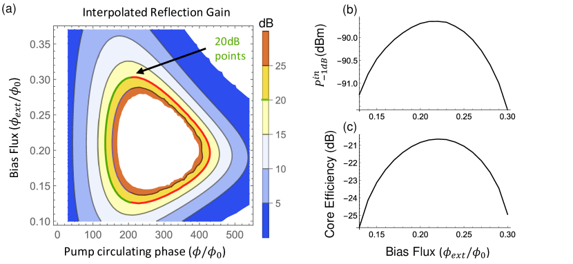
To calculate the pump power that produces dB gain, we apply a procedure similar to the tuneup of the real amplifier. At a particular flux value, we can turn up the pump power and analyze the gain of a weak signal. Repeating this process over a half-quanta of flux values produces a plot shown in Fig. A.2(a), showing a contour of gain points that are all viable bias points. We have divided this contour in two pieces, representing the lower pump power dB gain points in green, and the higher pump power points in red. Despite also looking like dB gain points, points along the red contour are not guaranteed stability and so we neglect them in the analysis, continuing with only the bias points along the green curve. To investigate the variation over the flux bias of the simulated amplifier, we move along the green contour, testing both the saturation power and the core power added efficiency
(which reduces to approximately at dB gain and near amplifier saturation) at each bias point of the amplifier, with the results shown in Fig. A.2(b)-(c). We find only weak variation in saturation power, but more pronounced variation in the pump efficiency at saturation.
The marginal variation is seen along the bias flux for saturation power, reinforcing notions put forward in [19] and [20] that the static Kerr of the amplifier mode does not act as the primary control of the saturation power, however the significant variation in pump power without a change in saturation power also complicates attributing saturation solely to pump depletion. It may be possible, for example, that the effects of Kerr and pump depletion are opposed to one another in how they affect saturation, with the low (static) Kerr bias points toward having more saturation power relative to the pump, but less pump power to draw from at dB gain. Continued study of this equation of motion is necessary to explain these effects in greater detail [40].
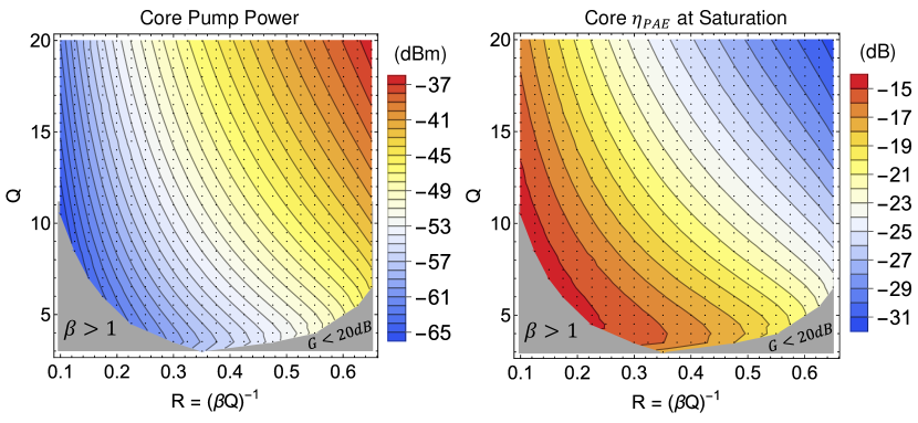
Lastly, we sweep through a significant subset of all possible families of amplifiers of this circuit type to investigate how both the pump power added efficiency and the pump power required to achieve dB gain vary. In Fig.A.3(a) we see that within a given gain family of amplifiers (a vertical line cut through either (a) it (b)), the required pump power increases with respect to the quality factor, and in general that the higher saturation power families of amplifiers determined by the x-axis coordinate require disproportionately higher pump powers at higher quality factors.
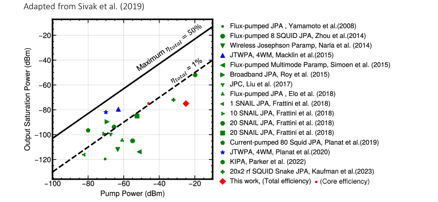
We can see this disproportionality directly in Fig.A.3(b), which shows that the pump efficiency drops significantly with higher quality factor and decreases yet more as one designs for larger and larger (higher and higher saturation power) . We note that despite the simulated pump efficiency of approximately dB for the parameters of our devices, the amplifier in this work performs worse in total efficiency, only achieving approximately dB pump efficiency because of the pump reflecting off of the coupling capacitor, discussed in Appendix B.
Appendix B Pump efficiency
The advantage of utilizing a 3-wave JPA over a 4-wave JPA is the ability to use a single pump at twice the signal frequency, generally reducing the pump leakage into the signal band of the readout chain and making it easier to implement filters to further reduce pump leakage. However, this advantage comes at a cost, which is that the behavior of the circuit near the pumping frequencies has to be carefully considered independently of the behavior at the signal frequencies. For example, it is possible that far away from the signal band it is challenging to get the pump tone to interact with the parametric core of the system that you are driving, significantly raising the pump power requirements of the amplifier and possibly heating the dilution refrigerator it resides in. Therefore, it is important to consider how effectively a certain input pump power drives parametric processes.
Generally, the efficiency metric that most directly impacts the surroundings of the JPA is power added efficiency (PAE) which expresses efficiency as a ratio of the output power at the signal frequency minus the input power at the signal frequency in ratio to the pump power at the pump frequency,
We have already simulated for the core of the amplifier (without the capacitive coupler) in Appendix A, shown in Fig. A.3(b), and so we will define another quantity that captures the difference between the input coupling at the signal frequency, captured effectively by the decay rate , and the pump frequency. This difference is not modeled in the periodic steady-state simulation, which uses the same decay rate for both signal and pump. To model the real circuit, which uses a coupling capacitor to alter the real part of the impedance on resonance, we will modify the "core efficiency" shown in Fig. A.3(b) by another factor which we will calculate as a function of any coupling impedance.
As detailed in Appendix A, the driving term we are concerned with is the circulating phase at the core node of the amplifier, which is the phase across the rf-SQUID array element. To model the effect of any arbitrary coupling series impedance, we consider the circuit below in Fig. B.1.
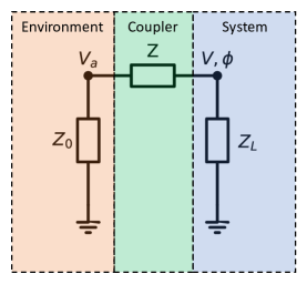
For the particular case of a series coupling impedance, the result is easily attainable by voltage division, allowing us to find the power dissipating in the real impedance outside the amplifier, given by , as a function of the impedances and the required circulating phase
where and are complex amplitudes for , respectively. This can be further simplified by assuming all-reactive loads and couplers , as is the case for a JPA coupled via a capacitor as long as the pump is not dissipating in the amplifier,
We can further group the pre-factors with and rearrange the equality to form an efficiency metric
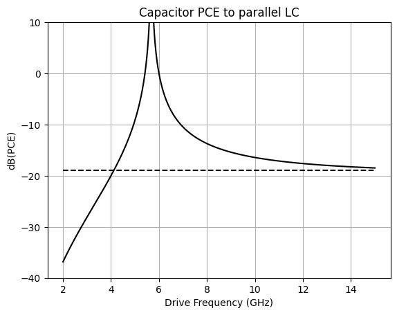
The efficiency that the core utilizes the pump which makes it to the core node is the topic of dedicated research of its own [40], so we define this simpler metric as phase coupling efficiency (PCE). This quantity allows the circuit designer to accurately anticipate the amount of pump power that will make it to the core of the amplifier under some assumptions, and serve as useful energy to the amplification process as opposed to being reflected off of the coupler. The phase coupling efficiency, pump efficiency, and targeted output saturation power combine to determine the total power requirement of the amplifier, the relevant quantity when considering heating problems in a dilution refrigerator.
| (5) |
There are some limitations to this simple calculation, the chief among them is that there must not be a zero in the denominator, or else the efficiency diverges positively at that particular frequency. At first, this appears to be a good thing. However, a positive divergence necessarily implies that the pump power to induce any phase across the load becomes arbitrarily small. This consequence is incompatible with a stiff pump, and so it appears that the PCE can only be evaluated far away from such poles.
This can be calculated for a coupling capacitor with reactance and is most useful in the approximation of driving far above resonance of the mode, where the load reactance of a parallel LC resonator is dominated by the capacitor . This gives a high-frequency limit to the PCE and graphed by the dotted line in Fig. B.2 of
Power-added efficiency is not usually the dedicated focus of JPA’s fabricated in academic settings, with the primary focus usually being on quantum efficiency, bandwidth, and saturation power in that order of priority. Nonetheless, we find it interesting to review the power-added efficiencies of many JPA’s in the field. We found the first such review in [19] very helpful for perspective on the topic, and so have edited it here with some additions. While we do not make similar distinctions for total versus core power added efficiencies for all devices, due to the many differences in couplers and three versus four-wave nonlinearities employed, we still find it helpful to gauge our device’s pump efficiency in reference to other devices fabricated in the field. With this in mind, we conclude that while the core efficiency is competitive at the level, the choice of pump coupler places the of our device below the norm.
The PCE and the PAE determine the total power requirement of the amplifier, and so future work will include coupler optimization to more effectively bring down the power requirement without creating too soft of a pump. Accounting for PCE will hopefully allow future devices to operate without the use of a hot pump line and diplexer.
Appendix C Experimental details
C.1 Fabrication
Our devices were fabricated at Boulder Microfabrication Facility (BMF) at National Institute of Standards and Technology using a Nb/Al-AlOx/Nb trilayer process with low-loss amorphous silicon (a-Si) as an inter-wiring dielectric as described in [25]. From the substrate up the nominal layer thicknesses are as follows: 381- -thick intrinsic Si wafer ( resistivity) with 200 nm Nb, 8 nm Al-AlOx, and 110 nm Nb forming a trilayer that is patterned top-down on the substrate to define Josephson junctions and the bottom Nb wiring layer. These structures are blanketed by 310-nm-thick a-Si dielectric layer. Vias patterned through the dielectric form contacts between the junctions, or bottom wiring, and the 300-nm-thick Nb deposited as a top wiring layer over a-Si. The top and bottom wiring layers together with the low-loss a-Si between them form thin-film parallel-plate capacitors. The fabrication was further modified from the description in [31] to insert a thin bi-layer (< 20 nm) of Nb/Al between a-Si and the top Nb wiring layer to facilitate improved patterning of layers and increase device yields. The full details of the fabrication will be provided elsewhere. The top Nb wiring is bonded onto an external PCB with 1% Al-Si wirebonds to carry signals off-chip into the external environment.
C.2 Lines and external circuit elements
From its single input port, the device is driven through two different lines via a frequency diplexer with a low-pass dB cutoff at GHz, a high-pass dB cutoff at GHz, and over dB rejection from the high-pass port to the common port at the frequencies in this data. The high-pass line provides the pump through a very lightly attenuated (dB attenuator at ) line, and the low-pass port receives the reflected signal from the cavity via the circulator and two Keycom 15 superconducting NbTi semi-rigid coax cables. The diplexer enables rejection of the thermal noise of the high-power pump line without losing pump power at the pump frequency at the cost of additional cabling and insertion loss of approximately dB from the diplexer, both of which must reduce the quantum efficiency of the measurement.
C.3 Flux biasing: offsets
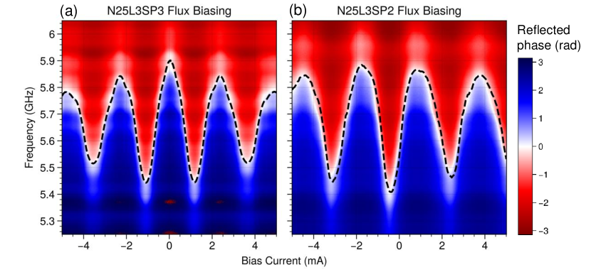
This amplifier is sensitive to external flux offsets caused by the earth’s magnetic field as well as other stray magnetic fields such as nearby ferrite circulators and isolators. In order to shield the device from such stray fields, the amplifier package is enclosed first by a thick 6061 aluminum superconducting shell and then again by a high permeability cryoperm shield made from Amumetal 4K. Despite these precautions, we are able to see distortions in some setups, such as flux offsets even when no bias current is running through the superconducting electromagnet used to bias the amplifier, seen in Fig. C.2(b). However, freshly annealed cryoperm cans are able to reject these external flux offsets effectively, shown for a different device in Fig. C.2(a) by the high degree of symmetry around zero bias current.
C.4 Flux biasing: tunability
One factor that weighs on the choice of the quality factor in the design of the amplifier is the tunable frequency range over which the amplifier can achieve dB gain. Because of the low instantaneous bandwidth of a typical reflection JPA, their chief practical strength lies in their tunability to whichever frequency the readout cavity needs to be driven for measurement. Because the readout cavity frequency of a typical transmon qubit is fixed and designs vary over a few GHz for modern transmons, it is necessary to be able to tune the gain center frequency of the amplifier on the order of a few hundred megahertz or to broaden the amplifier’s gain response using an impedance matching circuit to minimize the number of separate amplifiers required to cover the entire readout band. Further, we observe that the amplifiers in the family that barely achieve dB gain shown on the right-hand side of Fig. 2 only achieve that gain in a narrow range of bias flux. Our devices are simulated to achieve gain for an array inductance of approximately to pH, which gives a nominal tunable range of approximately MHz measured from the maximum frequency.
In practice, however, the device achieves a much narrower tunable bandwidth than this, only about MHz, which can be seen in Fig.C.5(b). One would expect that perhaps the reduction in tunable bandwidth could arise from flux nonuniformity in the array, and so we analyze this possibility next.
C.5 Flux biasing: uniformity
Our high-power JPA is biased by the use of a superconducting electromagnet set into a cutout underneath the copper amplifier package. With a -scale distance from the plane of the array to the edge of the electromagnet solenoid and the finite radius of the coil of approximately , we anticipate that there should be very little flux nonuniformity in the array from the nonuniformity in the magnet field alone.
To investigate this, we sweep the current through the magnet over the maximum possible values without causing heating of the magnet loom connections in the refrigerator, then analyze a fast Fourier transform (FFT) of the resonant frequency modulation in Fig. C.3(b). We can then identify peaks in the spectrum in Fig. C.3(b). The transform correctly identifies the primary modulation frequency highlighted by a green vertical line about the peak value.
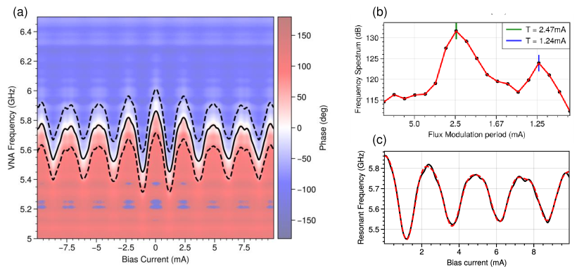
The origin of the second-highest peak is unknown. One possible explanation is that large superconducting planes at the boundaries of the array are shielding the first and last few rf SQUIDs from receiving the full external flux through their loops. This local shielding would be very similar on both the ground and resonator node boundaries of the array. In effort to remedy this, future efforts will include tapers to the array, diminishing the local effect of any adjacent superconductors.
C.6 Saturation power calibration
Power calibrations are often difficult to do in a straightforward way for devices at the base of a dilution refrigerator. Measurements of the input attenuation up to the plane of the amplifier at room temperature are easy, but they are often inaccurate, as all of the losses are susceptible to changes in temperature. The most straightforward way to calculate power for an amplifier serving to read out a qubit is to use the qubit as a power meter [30]. Independent measurements of the qubit can extract the frequency shift of the qubit per photon in the readout cavity. This allows qubit spectroscopy at varying readout powers to directly measure steady-state power in the readout resonator by watching the qubit shift in frequency. As we show in Fig. C.4(a), after establishing this baseline with the qubit, the only tasks remaining are to link the DAC drive voltage to a voltage on a spectrum analyzer. This is simple to do by simply removing the drive from the fridge and attaching it to a spectrum analyzer, a necessary step in eliminating mixer LO leakage and tuning single-sideband upconversion in any case. The results of these calibrations as well as a similar procedures for the VNA are shown in the remaining subplots in Fig. C.4. In our case, the conversion loss of the upconversion mixer and the cable losses are roughly balanced by the additional amplification in the chain.
C.7 Saturation power variation over bias points
Many amplification schemes focus on the available bandwidth of the amplifier. Considering resonant JPA’s without matching networks typically lack instantaneous bandwidth, they typically need to be flux tuned to different operating points, and the pump moved in frequency, in order to achieve gain at a variety of frequencies. A figure of merit of such a device is the tunable bandwidth - the range where the amplifier can operate when allowing for any possible tuning. Because changing the flux bias and pump tuning of the amplifier likely affects the saturation power of the amplifier, we measure multiple bias points distributed over the rf-SQUID JPA’s tunable bandwidth of approximately MHz.
C.8 High power measurement transitions
A natural next step in qubit measurement with a high-power JPA is to increase the power of the measurement to attain a higher integrated SNR with a shorter measurement time. While the amplifier is more than capable of handling the additional power, up to several hundred photons at this readout resonator frequency, the readout resonator plus qubit system is certainly not, as discussed in the main text. Here we show an example of how this process can go awry by showing integrated readout histograms.
In Fig. C.6(c) and (d) we give just one example of the measurement results one might expect to see when measuring at powers where the QND nature of dispersive measurement breaks down because of measurement-induced transitions in the qubit state. Transitions, which are visible as the “tracks” between states, increase in frequency at higher powers, as noted in multiple other publications [4, 5, 6, 7]. In particular, we even see transitions that are supposed to be forbidden, as well as many multi-photon transitions.
