From design to device: challenges and opportunities in computational discovery of p-type transparent conductors
Abstract
A high-performance p-type transparent conductor (TC) does not yet exist, but could lead to advances in a wide range of optoelectronic applications and enable new architectures for, e.g., next-generation photovoltaic (PV) devices. High-throughput computational material screenings have been a promising approach to filter databases and identify new p-type TC candidates, and some of these predictions have been experimentally validated. However, most of these predicted candidates do not have experimentally-achieved properties on par with n-type TCs used in solar cells, and therefore have not yet been used in commercial devices. Thus, there is still a significant divide between transforming predictions into results that are actually achievable in the lab, and an even greater lag in scaling predicted materials into functional devices. In this perspective, we outline some of the major disconnects in this materials discovery process — from scaling computational predictions into synthesizable crystals and thin films in the laboratory, to scaling lab-grown films into real-world solar devices — and share insights to inform future strategies for TC discovery and design.
I Introduction
Many advances in renewable energy technology are limited by the quality and availability of materials. Conversely, materials advances enable technological advances. The search for p-type transparent conductors (TCs) exemplify this: achieving a p-type TC with comparable properties to n-type transparent conducting oxides (TCOs) could enable new solar cell architectures and transparent electronics applications, serving as hole-selective top contacts or electrodes, buffer layers, back contacts for bifacial solar cells, and window layers in tandem devices.[1, 2] Many candidate p-type TCs have been proposed and explored, such as delafossites \ceCuO2[3] and \ceCuI,[4] among others. Yet the realization of high-performing p-type TCs is still a major research challenge, and p-type TCs for photovoltaic (PV) applications remain limited. This is in part due to fundamental physical trade-offs of combining transparency, p-type doping, and high hole mobilities in wide band gap oxides.[5]
While the first p-type TCs have been found by serendipity and following chemical principles (e.g., Cu-based TCs), it is now possible to identify new p-type TCs using first principles computations and high-throughput screening. “High-throughput” computational screenings usually begin with selection of a set of input compounds often from material databases (e.g., Materials Project[6], AFLOW[7], OQMD[8], among others), followed by a series of filtration steps using computed descriptors which represent proxies for certain materials properties.[9]
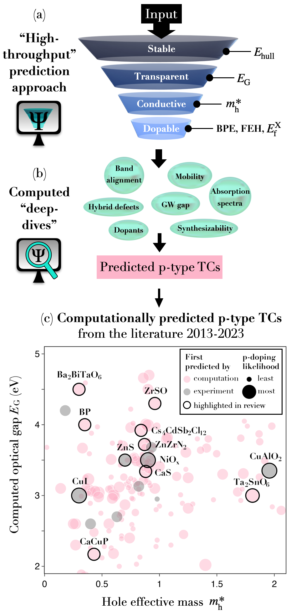
As depicted in Figure 1(a), after selection of inputs a typical screening method for p-type TCs starts with (1) a proxy for thermodynamic stability (usually energy above convex hull, ), (2) a proxy for absorption edge above the visible regime (usually the Kohn-Sham band gap, ), (3) a proxy for high hole mobility (usually hole effective mass, ), followed by a series of more computationally demanding calculations for hole dopability, band alignment, synthesizability, and other properties.[10, 11, 12, 13] As final screening steps as shown in Figure 1(b), higher accuracy computational methods can be applied such as hybrid or GW computations (to better estimate transparency) or electron-phonon limited mobility (to estimate hole transport).
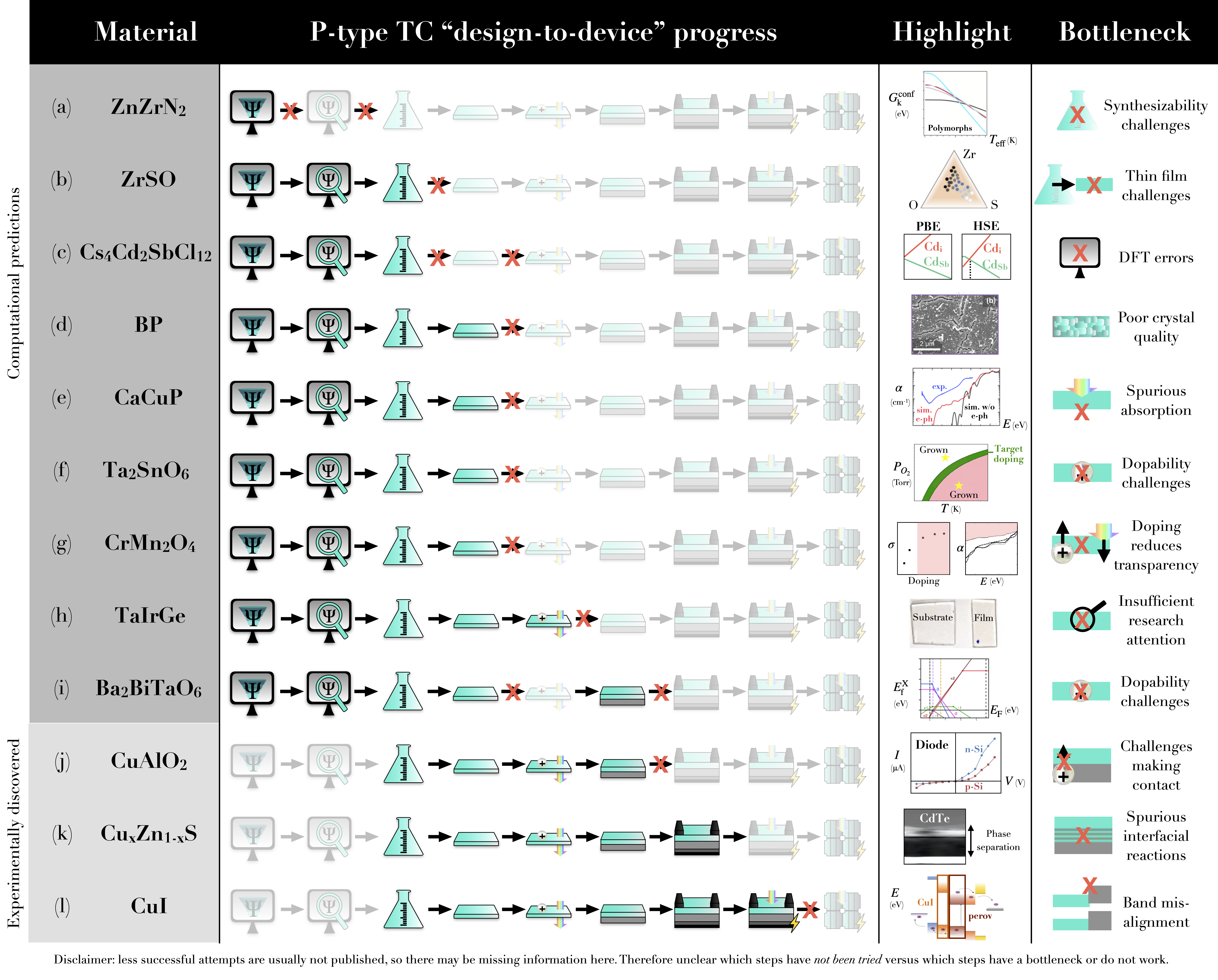
Computational screening research from the past decade has yielded promising p-type TC candidates, and key discoveries are summarized in Figure 1. One of the earliest studies focused on oxides and identified a handful new p-type TCO candidates.[10] Since then, a wide array of follow-up research has refined the screening criteria or input material set, for example by extending the chemistries of interest beyond ternary oxides or by focusing on specific chemistries or structures.[14, 15, 16, 17, 11, 18, 19, 20, 21, 22, 23, 24]. These studies have motivated the synthesis and characterization of a handful of computationally identified candidates, with a few notable success stories. For example, very high mobility and transparency have been observed experimentally in moderately p-type \ceBa2BiTaO6[15, 25] and \ceTaIrGe.[26] Transparency and high p-type dopability has been confirmed experimentally in \ceCr2MnO4, although with lower hole mobilities.[14] Overviews of experimentally realized p-type TCs can be found in existing literature reviews and benchmarking studies.[2] These successes, some of which are highlighted in Figure 5(c), are encouraging and bring a new level of predictability for computational materials science.
However, experimental confirmation of certain predictions has been either incomplete or not up to the expectations of the prediction. Boron phosphide (\ceBP), for instance, has been identified as a promising p-type TC with previous encouraging experimental results, but recent results indicate a difficulty to reach expected performances, as described later in this paper.[11, 27, 28] \ceTa2SnO6 showed promise yet could not be doped enough to measure hole conductivity.[29] Other predicted materials remain to be grown and evaluated, ideally in thin film form (e.g., \ceK2Sn2O3, \ceB6O, \ceNaNbO2, \ceBeSiP2).[10, 22, 30] Progress in the field of predicted n-type TCs serves as an indicator that advances in predicted p-type TCs are within reach; for example, as a success of a high-throughput screening, a new computationally predicted n-type TCO \ceZnSb2O6 has been recently confirmed by experiment with high doping and mobility.[31, 32] However, despite the many successes, scaling up predicted TCs for efficient optoelectronic device applications remains a major challenge, and a variety of disconnects have emerged.
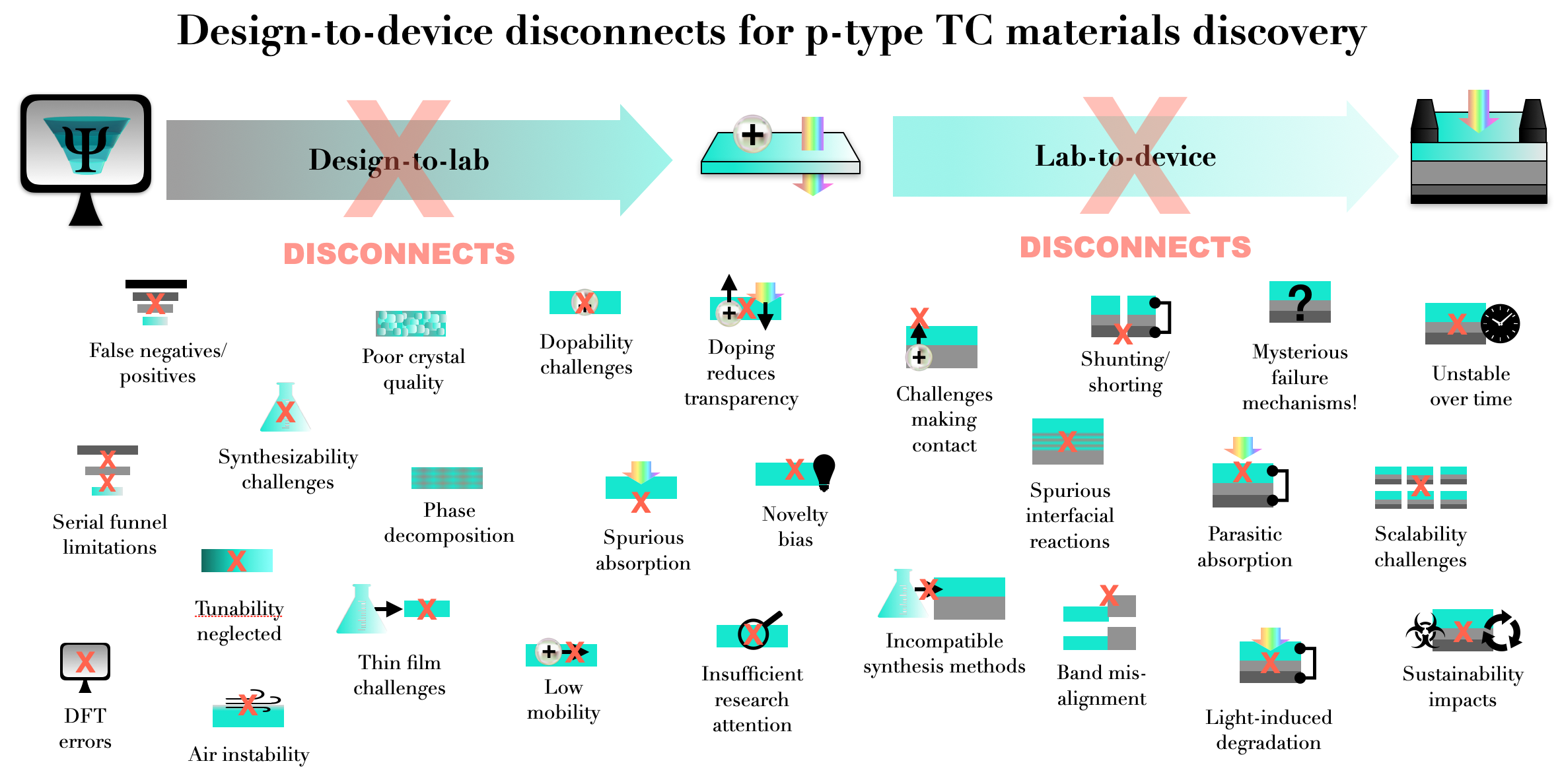
Historically, unwanted lab results and corresponding insights from researchers are usually not published, leading to a literature bias and a difficulty disentangling why disconnects are occurring. In this article, we identify and contextualize these disconnects observed in the literature and within our own research in scaling p-type TC predictions into PV devices. First, we design a framework for the different stages involved in this process, as summarized in Figure 3. Next, we highlight some of the most pernicious disconnects (see Figure 4). One set of disconnects stem from transforming predicted candidates into thin films in the lab: due to challenges including synthesizability, phase purity, dopability, and unwanted absorption, so far no predicted p-type TC grown in the lab performs on par with n-type TCOs. Another key set of disconnect arises from transforming predictions into scalable optoelectronic devices: challenges emerge such as making sufficient contact to the device, tuning band alignments, and growing interfaces free of defects, and other barriers. We also discuss specific barriers related to scalability and sustainability. Lastly, we offer guidance on how the research community can overcome such disconnects to bring our predictions into fruition in p-TCs and beyond.
II Materials design-to-device framework for p-type TCs
II.1 PV applications of p-type TCs
While conventional silicon (Si) solar modules do not typically include contact layers, emerging or “disruptive” PV such as silicon heterojunction (SHJ), tunnel oxide passivated contact (TOPCon), thin film (e.g., CdTe and perovskites), and tandem PV require various contact and buffer layer configurations to transfer charge carriers throughout the device. The current market share of PV (as of 2023) is mostly conventional Si, however various projections show that meeting our net zero requirements by 2050 will likely require rapid development and scaling of such emerging PV technology.[33]
One recent projection even expects “disruptive” PV deployment to ramp up rapidly after 2030, and by around 2040 become dominant over conventional Si.[34] However, as researchers develop these new configurations, few options for inorganic p-type transparent contacts are available, which limits architectures and performance. Therefore, developing appropriate contact materials for emerging PV, especially p-type transparent contacts, is an important research direction.
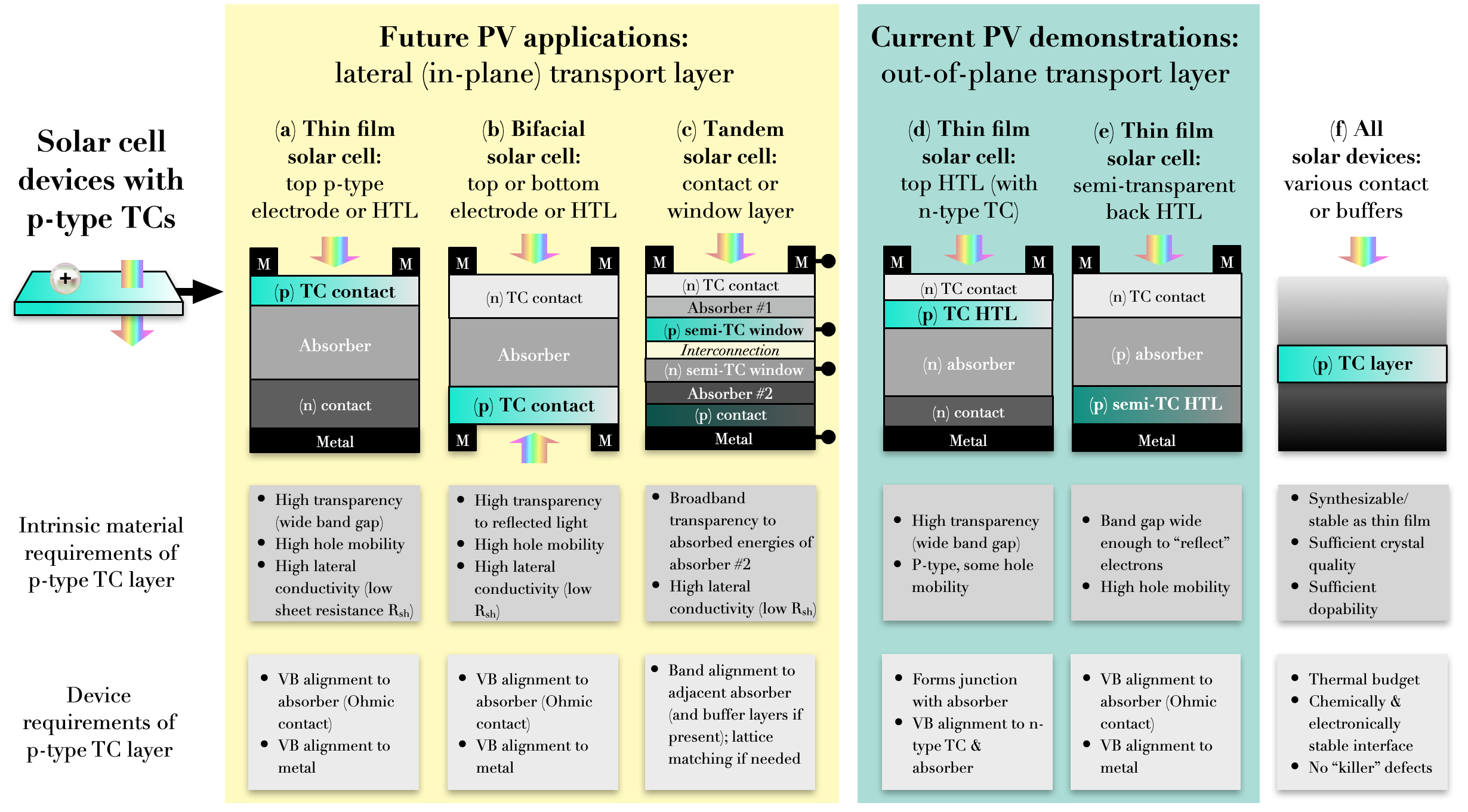
Applications for p-type TCs span far beyond solar (e.g., flat panel displays, transparent electronics, etc.), but for the purposes of this article we focus mainly on PV devices. Within the field of emerging PV, p-type TCs with different properties could serve a variety of roles. For example, p-type TCs could have a double role, that of a hole carrier selective contact (where a high work function is required) and that of a transparent electrode (where a low sheet resistance is required, usually below 100 /sq). As a selective contact, the p-type TC would extract photogenerated holes in the absorber material, and, as transparent electrode, it would laterally transport the carriers to the device terminal. Since the material is transparent, it would also function as a window layer in the device. This would enable novel device architectures for e.g., bifacial and semitransparent PV, which currently relies exclusively on the use of n-type ITO. Representative device designs are summarized in Figure 2, with future applications enabled by high-performance p-type TCs highlighted in yellow in (a–c). Designing TCs with high lateral (or “in-plane”) transport for these applications will be the focus of this paper. For reference we also show two “out-of-plane” transport configurations (d-e) in which mobility and dopability are less important, buffer HTLs and semi-transparent contacts (in which transparency is less important); since these applications have actually been demonstrated, they will be used to showcase challenges scaling to devices in the “Lab-to-device disconnects” section, but are not the focus of this paper. This variety of applications is the origin of one important disconnect, which arises from an intermingling of problem statements during the materials design stage. Namely, a material predicted from an application-agnostic screening for p-type TCs may not be appropriate to use in a specific application, e.g., might not provide an adequate band alignment.
II.2 Materials discovery stages
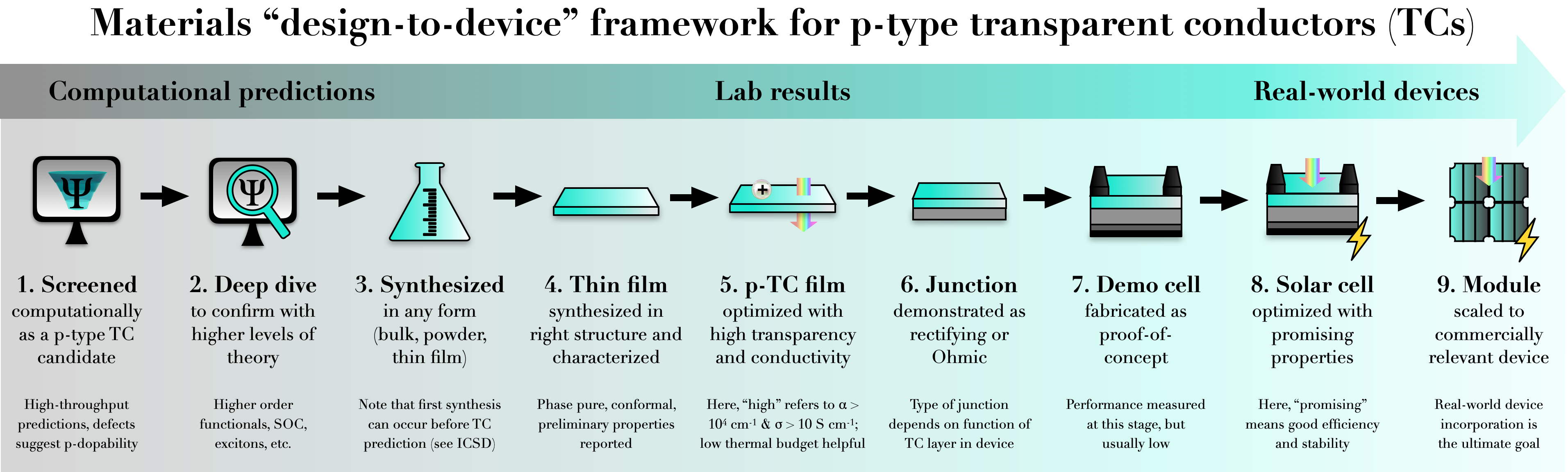
To understand the disconnects that emerge when scaling up computationally-predicted materials, we first summarize the main stages involved in going from a predicted material, to a synthesized material, to the exploration of its functionality on a device, and to a commercially-relevant device. For the specific case of a p-type transparent conductor (p-type TC), the “design-to-device” framework is summarized in Figure 3 with the following nine key stages:
-
1.
Computational screening: As shown in Figure 1(a) a material is “screened” as a promising candidate, often from a database. Simple computational metrics representing properties of stability, transparency, and conductivity are evaluated. Usually a stoichiometric, well-defined crystal structure is assumed, though high-throughput defects have started to emerge and could be used at this stage.[35, 36] Various biases can occur at this early stage that introduce disconnects at later stages.
-
2.
Computational deep dive: Higher levels of theory (e.g., spin-orbit coupling, GW) and more in-depth analysis methods are applied to more accurately predict properties of synthesizability, transparency, temperature-dependent mobility, carrier concentration from defects, and device-relevant parameters such as band alignment, as shown in Figure 1(b). Structural models can be more complex at this stage to account for off-stoichiometric and non-equilibrium effects.
-
3.
First experimental realization: The material is synthesized for the first time, usually in the form of a bulk single crystal or powders (e.g., using solid state synthesis or mechano-chemical synthesis). From powders or single crystals it is possible to confirm crystal structure, stoichiometry, air and moisture stability, and preliminary properties, though at this stage optoelectronic properties are not usually assessed. When screening from a database of known materials such as ICSD, this stage has often already been realized, so occurs before stage 1.
-
4.
Thin film synthesis: The material is synthesized as a phase-pure, conformal thin film. There are numerous methods to fabricate thin films, from wet synthesis to chemical or physical vapor deposition, in one or multiple steps. Thin film formation can result in epitaxial (single crystal), polycrystalline or amorphous films. The microstructure, thickness, stoichiometry, point or crystallographic defects, and surface effects will strongly influence the thin film properties and functionality. Specific synthesizability challenges and disconnects for p-type TC thin films have been discussed previously by Fioretti and Morales-Masis. [37]
-
5.
Thin film optimization: A p-type TC film is optimized, with high transparency and conductivity (the first reported film in stage 4 is usually not indicative of how much performance can be tuned). Such optimization can occur through doping, alloying, or optimizing process conditions such as annealing, among other methods. Throughout this manuscript, “high” transparency refers to cm-1 and “high” conductivity refers to S cm-1, though what is considered sufficiently “high” depends on application. We note this stage is often skipped for novel p-type TCs.
-
6.
Junction demonstration: A p-type TC is demonstrated to form a junction with another material, either deposited directly on an active substrate or on top of a device stack. The key challenges at this stage are chemical and thermal compatibility (e.g., to avoid chemical intermixing at interfaces or material degradation) and electronic alignment (e.g., valence band energies aligned), as well as good physical adhesion, without degrading the junction partner material.
-
7.
Solar cell demonstration: The p-type TC film is incorporated into a full solar cell device stack with demonstrated performance. Often this first device has low efficiency and poor device characteristics. p-type TCs can be deposited directly on a substrate or on top of the device stack (depending on the device polarity). The substrate or device stack will define the limitations for the p-type TC film deposition, such as thermal budget. This in turn will influence (or limit) the final properties of the p-type TC film.
-
8.
Solar cell optimization: The solar cell is optimized around the p-type TC layer, with reasonable PV performance values such as open circuit voltage, fill factor, and efficiency. At this stage, in addition to retaining good thin film properties and optimizing the TC, the interfaces play a key role in device performance. One way this disconnect can be alleviated by including interface simulations once the device stack is known (e.g., as done for organic and halide perovskite solar cells).[38]
-
9.
Scaling device to module level: Scaling up lab-scale devices (solar cells) into commercially-relevant devices (solar modules) requires different fabrication techniques for TCs, and can change properties and requirements. As reported in NREL’s well-known PV efficiency charts,[39, 40] solar cell properties often cannot be reproduced on the module scale, due to various disconnects such as conformality and processing constraints. At this stage, supply chain, cost, and sustainability factors also must all be considered. The ultimate goal of materials discovery is to go from a predicted material to this final stage.
This framework will be used throughout this manuscript to guide our exploration of disconnects. These steps are inspired by the technology readiness level (TRL) framework, which will also be referred to when appropriate, however our steps 1–6 expand upon earlier stages of materials design. This framework is designed and adopted specifically to address stages of materials discovery in p-type TCs. We emphasize that discovery does not necessarily follow this linear flow: often, optimization involves iteration between these stages. Historically, most materials have been synthesized first before computational predictions, and many recent studies return to computational “deep dives” after experimental stages to fill in experimental knowledge gaps or inform decisions. To highlight representative materials discussed throughout this paper, Figure 5 illustrates the stage along the “design-to-device” framework in which research and development is stalled, a graphical highlight of research at this stage, and one of the key disconnects describing why progress is stalled.
III Design-to-lab disconnects
In this section, we outline key disconnects that emerge going from the prediction of a new p-type TC (stage 1) to the realization of optimized properties in an experimental p-type TC thin film (stage 5). Some common disconnects at this stage are summarized in the left-hand side of Figure 4. We will also discuss strategies to confront these challenges.
III.1 Computational screenings contain limitations and biases
First principles computations are powerful but have inherent fundamental limits and numerical dangers such as convergence that need to be kept in mind. We will assume in this discussion that computations have been performed by an expert, achieving the necessary numerical convergence for the targeted task. We will also assume that the inherent limits of the approximation used (e.g., semilocal DFT underestimates band gap and affects defect computations dramatically) are taken into account in the screening process. Unfortunately, a small fraction of studies in the field do not follow these requirements and we warn the reader to always question whether computational results have been interpreted with caution and the right amount of expertise.
The efficacy of high-throughput computational screenings emerges from the quality of its input data, which usually comes from computational databases or the ICSD. These repositories have grown substantially, encompassing diverse materials and properties. However, extensively studied materials are over-represented in these databases, which can induce a selection bias toward well-studied candidates and can potentially neglect less-studied ones. For example, previous literature suggests non-oxides as promising p-type TCs due to low effective masses and low ionization potentials.[11] However, there are far more oxides than non-oxides in materials databases, so non-oxides are under-sampled in screening studies.
An algorithmic bias can lead to prioritizing properties that are more readily calculated or accessible, potentially overlooking properties that may be more representative of desired performance. In order to reduce the input materials to a manageable subset, the initial steps of computational screenings usually filter with property proxies that are computationally inexpensive (“cheap”) to calculate. For example, although both effective mass and scattering time contribute to achieving high mobility, given current algorithms (“cheap” proxy) is much easier to calculate than (“expensive” proxy). Additionally, hole conductivity depends on doping density which is also difficult to compute. Therefore, we are biased towards looking for materials with low rather than those with excellent scattering or doping properties, and we need to be careful about how close a cheap proxy correlates to an expensive proxy.
Similarly, a knowledge bias occurs when a model or analysis is limited by existing knowledge and fails to account for emerging or unexplored factors. For example, screening for low effective mass and wide direct band gap as shown in Figure 1(a) is appropriate for traditional TCOs that behave as doped semiconductors following a rigid band model (e.g., \ceZnO, \ceSnO2). More recently proposed mechanisms such as polaronic TCs,[9] intrinsic TCs[41], or TCs containing forbidden transitions[30] are less likely emerge from this approach, however this can be remedied when new mechanisms are understood and can be incorporated into the screening.
Once screening criteria are chosen, a threshold bias can arise from selecting cutoffs, their tolerances, and criteria priorities, as these thresholds often lack objectivity. For instance, picking a cutoff for “low” hole effective mass () is typically arbitrary; opting for only the lowest could exclude highly transparent materials, and the needed to achieve a certain high mobility depends on material physics. Additionally, there is a lack of threshold standardization regarding how defect calculations are performed and interpreted. While serial screening is common, Pareto analysis or multi-objective optimization can counter threshold bias and improve outcomes.[42] However, one key challenge is selecting appropriate weighting parameters formally and quantitatively. Such optimizations become application dependent and are rarely done for p-type TCs.
Lastly, biases can occur when reporting computational results. Novelty biases can lead to publishing and highlighting new and exciting findings, while negative or non-novel outcomes are not usually reported. Screening studies tend to report “new” p-type TC predictions rather than reporting whether past predictions have been corroborated. However, especially given challenges to synthesizing predictions in the lab (see next sections), it would be extremely useful for experimental researchers to know whether a result has been computationally reproduced by multiple groups and different methods.
Together, these biases can lead to false negatives and false positives emerging from screenings. Input sets and screening criteria need to be judiciously selected and appropriately communicated to avoid misleading predictions. Although false negatives are challenging to address, false positives can be mitigated by performing a computational “deep-dive” (stage 2) before attempting synthesis. As an example from our research, shown in Figure 5, sputter synthesis was attempted (stage 3) shortly after \ceZnZrN2 emerged from a p-type TC screening (stage 1), before a thorough computational assessment (stage 2). The target phase could not be synthesized, and by turning back to a “deep dive” it was hypothesized that due to disorder intolerance the selected synthesis method would likely have never yielded this phase.[43] In general, experimentalists using screenings to inform their research should be aware of how such biases propagate and how to carefully scrutinize the extent of computational findings before going to the effort to grow it in the lab.
III.2 Predicting synthesizability and stability can be challenging
III.2.1 Bulk crystal synthesis
The next disconnect is that many new p-type TCs have been predicted, but not all have been successfully synthesized in the laboratory in the desired crystal structure (stage 3 in Figure 3). One likely reason for the lack of reported synthesis is that many have not been attempted yet, or if attempted have not been published possibly due to negative results (so-called “dark reactions”[44]). Computational databases tend to report whether a given material has been synthesized previously (pointing to the ICSD), and bulk or powder synthesis is most common. One approach to avoid assessing synthesizability is to simply restrict input datasets to just these known experimental materials. However, some exciting new predictions of p-type TCs do not yet have any reports of synthesis, e.g., \ceCs2 (=S,Se,Te)[18] and double perovskites such as \ceCs4^2+^3+2^VII12,[45] so for these materials synthesizability should be judiciously assessed. We will start by discussing challenges that have arisen with growing hypothetical crystals that have not yet been synthesized in any form.
Accurate assessment of whether a hypothetical material is actually synthesizable and stable is not trivial. The first disconnect arises from the crude assumption that the descriptor is a good proxy for synthesizability. Namely, it is generally assumed that materials with formation enthalpies at or near the ground state energy predicted by DFT at zero Kelvin ( 0 eV/atom) are the most likely to be experimentally realized, while materials with 0 eV/atom are less likely to be synthesized.[46, 47, 48] itself is impacted by errors in DFT and correction schemes, and does not include entropic effects. Various low-cost approaches to estimate vibrational and configurational entropy in computational screenings have emerged,[49, 50] which can be incorporated screenings. Additionally, assessing dynamic stability is essential,[51] and synthesis is driven by kinetics as well as thermodynamics. Despite many recent first-principles and machine learning (ML) efforts to address kinetics via synthesis pathways,[52, 53, 54, 55, 56, 57] such as solid-state reaction networks,[58, 59] a deeper understanding and predictability is still needed; increasing efforts in automating synthesis may help address this challenge.
Specific synthesizability challenges can arise due to the complexity of compounds selected as p-type TC candidates.[60] Many predicted TCs are multinary materials, since multiple elements provide an increased search space and tunability.[61] For instance, \ceCuAlO2 (often considered the first p-type TC) can be considered a ternary counterpart to p-type \ceCu2O in which Al increases the band gap,[62] and similarly \ceBa2BiTaO6 a quaternary extension of p-type \ceBaBiO3 in which Ta increases the gap. Furthermore, binary TCs can be extended into multinary solid solutions to enhance performance, such as recent S incorporation into CuI.[63, 64, 65] However, more elements can induce challenges in synthesizability including increased likelihood to phase segregate, as well as complex disorder and defect configurations.[60, 48] For example, one challenge that has stalled progress in thin film synthesis of predicted p-type TC \ceZrOS[10] has been phase separation into defective binary phases \ceZrO_x and \ceZrS_x, as it is challenging to introduce S into \ceZrO_x (see Figure 5).[37] Another well-known example of such challenges can be observed in quaternary and quinternary kesterite PV absorbers, which tend to easily phase separate.[66]
Even if reported as “synthesized” in the ICSD, many compounds are not stable in air or moisture. For example, \ceK2Sn2O3 was predicted as a p-type TC by Hautier et al.[10], but rapidly degrades in air. Air instability does not completely rule out a candidate, but using such materials in a device and even measuring them introduces serious challenges. For example, SnO and AgI are unstable in air, but have still been explored for device applications. CuI can also present stability challenges when exposed to air, presenting variations in conductivity due to iodine loss or Cu-oxidation. However, this depends strongly on the fabrication method and solar cell process used. [67, 68, 69] Non-oxides in particular tend to be less stable in air; some are protected by a passivation layer, while others can fully decompose or oxidize. The descriptor “energy above the Pourbaix hull” (), based on Pourbaix diagrams, can be used as a thermodynamic check for air stability.[70] Another recent method uses a “greedy algorithm” to assign heats of oxidation to screen for in-oxygen environmental stability and heuristically determine whether a material may self-passivate.[71] However, to our knowledge there is no extensive benchmarking to show that that these metrics are predictive of experimental instabilities. In our experience, especially with non-oxide TCs, p-type TC candidates predicted stable by and even have still degraded in air. Air instability may be a key reason why progress in non-oxide p-type TCs has been limited.
III.2.2 Thin film synthesis
Specifically for TCs, another set of disconnects arises going from bulk synthesis to thin film synthesis (stage 3-4). Computational predictions are generally derived from bulk, periodic calculations at thermodynamic equilibrium, whereas in practical applications p-type TC materials are thin films, contain multiple types of defects, and are usually synthesized using non-equilibrium growth techniques. Sometimes these assumptions hold and, for example, a predicted structure can be grown as a thin film with properties corresponding to predictions, as demonstrated by various success stories such as \ceBa2BiTaO6 and \ceCaCuP.[15, 72] However, this is not always the case; the effects of surface energies, surface termination, strain, and texturing in thin films can influence which phase is stabilized at a given condition, and can yield a range of properties far beyond the single observable value predicted for the bulk structure. Additionally, amorphous thin films are difficult to simulate, though many high-performing n-type TCs are amorphous.[47]
Similarly, different thin film synthesis methods can result in an extensive span of structural properties that can deviate from predicted bulk properties. However, there is not yet a framework such that an ideal synthesis route and tool can be selected from first principles alone. The synthesis pathway prediction algorithms mentioned previously are a step in this direction, but these assume thermodynamic equilibrium and are method agnostic (many polycrystalline thin film synthesis methods are non-equilibrium). From the experimental side, the synthesizability challenge is to grow thin films that can tolerate defects in microstructure, surface effects, grain boundaries, strain, dislocations, etc., while retaining properties simulated from single crystalline materials (see next section).[12] In sputtering, a technique commonly used for exploratory synthesis as well as for commercial TCOs, in some cases the “effective temperature” at the surface of a growing film have been shown to be more predictive of synthesizability and structural properties, rather than the chamber temperature.[43] One disconnect here is simply that in stages 3 and 4, not all synthesis pathways have been sampled. Confirmation biases can arise if researchers try one approach, encounter difficulties, and then decide to abandon the material altogether without exploring alternative approaches to access a different region of configuration space.
III.3 Origin of the mismatches between theoretical and experimental optoelectronic properties
If a predicted p-type TC can be successfully synthesized as a thin film (stage 4), the next challenge (stage 5) is to experimentally achieve predicted properties of interest such as high optical transparency and high hole mobility and concentration. Yet in some cases of predicted p-type TCs grown in the lab, at least one of these properties falls short of the computationally predicted ideal. There may be three reasons for these disconnects: (1) limitations of high-throughput descriptors in accurately estimating the optoelectronic properties, (2) differences in material properties between an ideal bulk crystalline material (the object of computational modeling) and a practically realizable thin-film material, and (3) extrinsic experimental issues negatively influencing the predicted properties of a thin-film material.
III.3.1 Accuracy of high-throughput optoelectronic properties
First-principles calculations are useful to approximate experimental properties, but they also come with caveats. In general more “expensive” calculations improve accuracy, but there are still limits and trade-offs. Rather than review computational methods to screen for p-type TCs, which has been done in depth elsewhere,[12, 13, 73, 2] here we will highlight a few key limitations to computing transparency, mobility, and dopability in bulk crystalline materials. We note, however, that the most efficient high-throughput approaches are built using a tiered screening approach where cheap methods are used first to select materials (taking into account their lower accuracy) and more accurate and expensive methods are used for the final candidates before moving up to experimental verification (see Figure 1).
A wide band gap is a central property of a TC. While “traditional” semilocal DFT is known to significantly underestimate band gaps (sometimes by 1 to 2 eV),[74] many more accurate methods with different levels of costs are available nowadays such as GW or hybrid functionals.[9] Some of these methods have already been used in a high-throughput fashion and machine learning is speeding up the assessment of high accuracy band gaps with minimal computational cost.[75, 76, 35, 77] Beyond the accuracy of the method, one needs to keep in mind optical gaps are not electronic gaps. A better estimate of the optical gap can be obtained using relatively cheap independent particle approximation (IPA) computations on top of DFT or hybrids. These computations will take into account the transition dipole moment for optical absorption (i.e., the oscillator strength) with possible forbidden or weak transitions. Some important TCs such as \ceIn2O3 rely on forbidden transitions for their high transparency.[78] Recent high-throughput work including in the TC field has started including these optical absorption computations, and p-type TCs with forbidden transitions have recently been proposed.[30] We note that more expensive approaches beyond IPA such as TD-DFT or Bethe-Salpeter equations (BSE) can be used to provide more accurate optical absorption, but in general, TCs with a band-like conduction mechanism have effective masses and band gaps that lead to small excitonic effects (exciton binding energies of around the tens of meV).[79]
To model transport, effective masses () that can be obtained from DFT or higher order theories are most commonly used as a proxy for carrier mobility. While effective masses vary between semilocal DFT and more accurate methods, the difference is usually small enough for semilocal approaches to suffice, especially when using for screening and as a proxy for mobility. While is a simple concept for conventional single-parabolic band materials, real materials can be anisotropic and have complex band structures with several competing bands.[9] Discrepancies between computed values of for the same material in the literature often come from different crystallographic directions or bands. When used as a proxy for mobility, it is important to consider all the possible bands involved in transport and average them out. Otherwise, picking the highest curvature band tends to underestimate the effective mass. In the last five years, the full computation of mobility has made enormous progress. Codes such as Perturbo,[80] EPW[81] and ABINIT[82] have well-documented and tested open source codes that fully compute phonon-limited mobility. These comprehensive approaches have been even scaled up and can be used to compute hundreds of materials automatically.[83] They remain expensive however, and simpler approaches assuming simplified scattering processes have emerged such as AMSET, which also provides a high quality open source code.[84] Errors of around 20% compared to experimental mobilities have been reported for these approaches based on electron-phonon and Boltzmann transport theory.[84] The field of TC design has already started to use these methods in recent studies. [32, 72, 30, 85, 23]
Finally, defects are essential to understand and predict p-type TCs. Point defects control doping and intrinsic defects can prevent p-type doping. Certain defects (e.g., oxygen vacancies) can act as “hole-killers” and prevent p-type doping. Due to the lack of automation and high computational cost, early high-throughput studies only computed defects as a “deep-dive” step after low and wide band gap materials had been identified.[10] However, since then automation has made huge progress and software packages have emerged such as pycdt and pylada that facilitate the generation and processing of input and output files (including charge corrections).[86, 87] Nowadays, key challenges stem not from automation but rather from the compromise between expensive, large supercell computations with hybrid functionals (which is the gold standard for defect computations) and the cheaper semilocal DFT-based approaches. While semilocal DFT can provide important information and has helped in first-stage screenings,[36] it remains essential to always verify these crude methods with a hybrid functional at the very least for the most promising materials. Indeed, similar to how semilocal DFT underestimates band gap, it tends to overpredict dopability, and its use without safeguard has led to false predictions of p-type doping. The field of high-throughput defects is moving fast with interesting developments in the use of methods compromising between DFT and full hybrid such as single-shot hybrid, as well as work on the more exhaustive search of the defect energy landscape.[88, 89, 90] In all cases, defect computations remain expensive and proxies have been highly sought out. Some recent studies have applied practical single-defect-based descriptors early in the screening, such as the hydrogen interstitial defect descriptor (“FEH”)[21] or the oxygen-vacancy formation energy descriptor.[91] Other studies have used branch point energy (BPE, or ) as a descriptor,[16, 18] but we caution against using BPE as its predicting power is questionable.[12]
III.3.2 Thin films properties can diverge from bulk properties
Practical TCs are normally required in the form of thin films with thicknesses on the order of a few hundred nanometers. Even if bulk properties are appropriately modeled, and if thin films can be grown, this requirement generates another possible source of disconnects between calculated and experimental properties (stages 4–5 in Figure 3). Most first-principles materials modeling methods assume a perfectly crystalline and infinitely periodic material. However, both assumptions often break down in thin film TCs, where non-equilibrium and nanoscale effects can dominate.[92]
Depending on the substrate and on the growth process, thin films can be epitaxial single-crystalline, epitaxial polycrystalline, non-epitaxial polycrystalline, and amorphous. Moving down this list, an increasing deviation from the properties of bulk single crystals is typically observed. The current generation of n-type TCs is either non-epitaxial polycrystalline (ITO, AZO, FTO) or amorphous (IGZO, ZTO, IZO).[93] Therefore, it is unlikely that epitaxial single crystalline films can practically be used as p-type TCs, both because of the much higher cost and the requirement of a suitable substrate, which is usually dictated by the application (see section “Scalability and sustainability”).
The TC-relevant property that is most often affected by imperfect crystallinity is carrier mobility. At a hole concentration of , single-crystalline silicon has a hole mobility of about , whereas mobility in polycrystalline Si with and grains are about and , respectively.[94] At an electron concentration of , typical electron mobilities of ZnO are for single crystals, for epitaxial films, and below for non-epitaxial polycrystalline films.[95] While the relative importance of grain boundary scattering decreases with increasing carrier concentration, grain boundary scattering can still remain a mobility-limiting mechanism even in the carrier concentration range,[95] so it is relevant for TCs. The lower mobility of non-epitaxial polycrystalline films with respect to their epitaxial counterparts can also be due to a higher density of both point defects and extended defects. These considerations do not invalidate the screening approach, with the understanding that the computationally-determined mobilities are generally upper bounds for the mobilities achievable by polycrystalline thin-films. Large crystalline bulk mobility is a necessary but not sufficient requirement as grain boundary scattering could be an issue.[96, 97] Although grain boundary scattering is difficult to model from first principles, various simplified high-throughput approaches have been proposed and applied,[84, 98, 99] and including it in screenings could be an interesting future avenue of research.
Another property that can be affected by imperfect crystallinity is optical transparency, especially when the fundamental band gap of the material is indirect and located at visible (rather than UV) wavelengths. In these cases, applicability of the material as a TC relies on the weakness of indirect optical transitions, resulting in negligible absorption in a thin-film sample because transitions involve both a photon and a phonon. Deviations from perfect crystallinity due to, e.g., closely spaced grain boundaries, extended defects, and inhomogeneity, are expected to relax the requirement for phonon participation in these transitions and, hence, increase the material’s absorption coefficient. The increase in the absorption coefficient of silicon between its indirect and direct band gap with decreasing crystalline quality is a well-known example.[100] A similar effect has recently been observed in polycrystalline BP and CaCuP films, predicted p-type TCs with direct gaps much larger than indirect gaps.[72, 28] In both cases, the experimentally reported absorption coefficient in nanocrystalline films is much higher than the calculated absorption coefficient using hybrid functionals and electron-phonon coupling, rendering them non-transparent.
Due to the requirement of inexpensive, large-area thin-film samples for TC in PV applications, such non-idealities might be unavoidable in practice. One may argue that that some detrimental effects of polycrystallinity may vanish for large crystal grain sizes in the m range, which can often be achieved in thin film samples, including In-based TCOs.[97] For some TCs such as ZnO, FTO and large-grained CuI, optical scattering effects typically become more prominent with increasing grain size due to an increase in surface roughness. This is visually manifested as a “haze” effect, which can be beneficial in thin film PV for light management, but could also result in low transmittance.[101] For reference, the grain size of commercial ITO films (n-type TCs) is often below .[102, 103]
One overarching disconnect between bulk and thin-film materials follows from the fact that many thin-film growth techniques operate under strongly non-equilibrium conditions, where thermodynamics-based modeling methods may not be appropriate. Some examples are plasma-based techniques such as sputter deposition, pulsed laser deposition, and plasma-assisted chemical vapor deposition. Interestingly, these are some of the most commonly used deposition techniques for TCs, partially because the presence of energetic species in the plasma can promote higher dopant solubility at low temperatures. In these types of processes where both ions and neutral species are present with a range of energies, the atomic chemical potentials used in the calculations of defect formation energies are not easily translated to experimental process conditions. Thus, the dopability of a TC may be significantly different than expected. The mobility may also be affected, since it is often limited by defect scattering in highly doped materials.
III.3.3 Challenges optimizing thin film growth and defects
Early synthesis attempts usually result in low- quality properties, which can be optimized and tuned with increased research efforts. For example, in the first reports of thin film n-type ITO in the 1970s conductivity was approximately 300 S cm-1,[109] but after two decades of intensive research conductivity was optimized to nearly 2 orders of magnitude higher (with a record of 22,000 S cm-1[110]). Since most of the predictions of p-type TCs have been within the past decade and a given prediction has received far less attention than ITO, it is reasonable that development of predicted TCs that have been grown as thin films is stalled between stage 4 and 5 in Figure 3.
Growing a high performance p-type TC requires optimal control of growth conditions and thus chemical potentials. Many of the computationally identified candidates offer p-type doping only within a specific window of chemical potential. For instance, a well-adjusted oxygen chemical potential can be essential during growth, since highly-reducing conditions can create oxygen vacancies that compensate any holes. We note that this problem can be present even if an shallow acceptor is incorporated in the film. \ceBa2BiTaO6, for instance, shows limited p-type doping because of the presence of oxygen vacancies and Bi on Ta anti-sites.[105]
While computational screening uses some level of dopability, screening leads to focus only on materials that could potentially be p-type doped (i.e., that could exist in chemical potentials that are favorable for hole doping). There is not an easy relation between chemical potential and experimental growth conditions. While qualitative statements can be made — i.e., lower oxygen chemical potential will be obtained by working in reducing atmosphere — computations cannot tell what exact conditions (gas flow, temperature, etc.) to use experimentally. The computed chemical potential can be influenced by effects not taken into account (alloying, unknown phases or temperature effects). Similarly, source material impurities should be carefully checked; e.g., C and Si are dominant impurities in boron sputter targets, but are some of the most effective dopants in BP (Si impurities alone can lead to carrier concentrations .[28])
Any single growth technique will have limits in terms of attainable chemical potentials. A recent case in point is the growth of \ceTa2SnO6,[29] which has been computationally identified and reported as a potential p-type TCO (albeit with a small gap of 2.4 eV) and is highlighted in Figure 5(f).[104, 111] High quality single crystals grown by molecular beam epitaxy (MBE) did not yield any measurable conductivity, even after extrinsic doping attempts using K and Ti. The most likely reason for these failed doping attempts lie in the limits of oxygen chemical potential achievable in MBE. Oxygen vacancies act as hole-killers and need to be avoided under oxidizing conditions. However, the most oxidizing conditions available with this MBE process are still not oxidizing enough to enable p-type doping. It remains to be seen if other growth techniques will lead to p-type doping in \ceSn2TaO6, and similar effects likely occur in other p-type TC candidates.
For potential TCs belonging to non-oxide families, a common experimental challenge (besides air stability, discussed earlier) is to ensure low levels of oxygen contamination in the films. This issue is particularly difficult to address when the target TC material contains highly oxophilic metals, such as the ones from Groups 1, 2, 3, 4, and Al. To address this problem, we recommend including “oxygen tolerance” calculations of promising TC materials, i.e., the calculated formation energy of oxygen substitutional and interstitial defects as a function of Fermi level. If any of these defects is found to be a donor with low formation energy, oxygen contamination is likely to limit the p-type dopability of the material. The development of more general oxygen-tolerance principles would also be welcome. For example, one may expect that oxygen substitution on the anion site is a donor defect in pnictides (one more valence electron) and an acceptor in halides (one less valence electron). If this is correct, oxygen incorporation would be detrimental for p-type conductivity in pnictides but it might be benign or even beneficial in halides. Beneficial effects of oxygen incorporation have been shown for CuI.[112, 69] Furthermore, the formation energy of these substitutional defects might generally be lower in materials containing an anion with a similar ionic radius to O2-. Thus, one may intuitively expect nitride p-type TCs to be most negatively affected by oxygen contamination.[113]
As eluded to with these examples, optimization of TCs often involves introducing defects, disorder and off-stoichiometry in a tunable manner. Sometimes intrinsic doping is possible, but usually extrinsic dopants are needed to increase dopability. While most screenings include some consideration of dopability, often only intrinsic defects are considered, and detection of problematic hole-killers is targeted without providing the exact shallow dopant to use. However, in some cases dopants have been proposed, e.g., for \ceLa2SeO2 (Na)[16] \ceBP (Mg, Si, Be, C)[11], \ceBa2BiTaO6 (K),[105] and \ceCsCuO (Na, K, Rb),[91]. Our experience is that defect compensation is often more limiting than the discovery of a shallow acceptor. There are a few rare cases where, even if a material does not have strong compensation, issues still arise in discovering the ideal dopant (e.g., n-type \ceLa2Sn2O7[114]).
Moreover, screenings usually identify ordered compounds, but the best known TCs are off-stoichiometric solid solutions rather than dilute defects. For example, ITO is approximately 5–10 at. % tin, exceeding the dilute limit,[115] and Al content in Al:ZnO (AZO) is approximately 2%.[116] One workaround is to screen for cases in which a solid solution of the two compounds is amenable to high transparency. We have proposed this framework previously, and incorporated an “alloys database” tool to do so in the Materials Project.[117] Additionally, in some cases TC properties could emerge non-linearly from tunability. For example, in p-type \ceNiCo2O4 spinels [118] disorder has been shown to reduce the hopping barrier and actually lead to increased conductivity compared to that of the ordered structure.[119] Finding methods to appropriately model and screen for dopants and tunability early on (stage 1-2) rather than during experimental optimization (stage 5) could lead to p-type TC breakthroughs, but this has not yet been done in practice.
III.4 Novelty bias and confirmation bias
Conventional n-type TCs such as \ceZnO, ITO, etc., have had their growth techniques and properties fine-tuned over decades by international research teams and industries for numerous applications. Thus, it is unsurprising that the first results of a new predicted material may not have properties comparable to predictions. But, although it is unfair to compare a preliminary result with the a highly optimized result of n-type counterparts, this is still often done, and may lead to discarding a promising material that just requires optimization to show its real potential. Even if the target material is not synthesized in a particular study, this does not preclude the possibility of synthesizing these compounds using other techniques. Yet null results are usually not reported. This limits the ability for followup research to learn lessons from less successful results and for results to be reproduced to increase statistical significance, while increasing the chance of repeating mistakes and wasting resources. We have highlighted a few key exceptions; for example, Barone et al. reported being unable to synthesize conducting phases of \ceTa2SnO6,[29] but this report inspired follow-up calculations to suggest their MBE growth did not sample optimal chemical potentials.[120] To remedy this, amorphous \ceTa2SnO6 has been proposed,[120] and these studies inspire future work to explore different regions of phase space.
The initial synthesis of novel computationally-identified thin-film materials often entails sub-optimal growth conditions, such as chemical potential. This is particularly true for so-called “high-risk” novel materials, in which customized tools likely do not yet exist, necessitating makeshift adaptations of existing experimental tools. Often, growth chambers designed and previously (or concurrently) used for conventional materials like oxides are repurposed for the synthesis of multiple new materials. Such adaptations raise concerns about contamination, especially by volatile species like alkali metals, zinc, sulfur, or halogens, which can compromise the material’s synthesizability, quality and defect sensitivity. For example, growing p-type phosphide TCs in chambers also used for sulfides may adversely affect hole concentration. “Exploratory” tools such as combinatorial sputter chambers can offer a wide range of elements and tunability,[121, 122, 123, 124, 125] so they are particularly advantageous at stage 4 in Fig. 3. However, exploratory thin film growth chambers accommodating volatile species are not particularly widespread, which is a barrier to enabling synthesis of new predicted p-type TCs. Often when predictions are made, one of the limiting factors is finding a synthesis team willing to risk attempting a novel compound with possibly exotic elements. In spite of these challenges, new high-throughput materials synthesis methods are on the rise, and could enable faster progression from a predicted TC (stage 1) to an optimized thin film (stage 5).[126, 127, 56]
IV Lab-to-device disconnects
If a predicted p-type TC can be optimized to high performance in the lab, incorporating this material into an actual device will bring a set of new disconnects, some of which are summarized and schematically depicted on the right of Figure 4. Due to intrinsic disconnects from stages 1–5 and new interface challenges, so far very few predicted p-type TCs have been successfully reported as junctions and in solar cells (stages 6–9 in Figure 3). Not only are device reports of predicted TCs rare, but we were unable to find reports of any p-type TC included as a layer for lateral hole transport, i.e., “electrode” in (a–c) from Figure 2, even as a small-scale proof-of-concept cell (stage 7). The only exceptions are \ceNiO_x, which is not technically a p-type TC due to low hole conductivity (although a recent report suggested external dopants could increase higher hole transport[128]), and \ceCu_xS, which is not very transparent, and in both cases devices have very low efficiencies.[129] From our understanding, p-type TCs have only been reported in solar cells as out-of-plane transport layers stacked next to n-type TC electrode or as continuous metal layers, as in the HTL of Figure 2(d), or as a semi-transparent bottom contact as in Figure 2(e).
With these limitations in mind, in this section we reflect on some lessons learned from reported attempts to incorporate p-type TCs into PV-relevant devices as HTLs, generally following the device configuration shown in Figure 2(e). We use insights from several p-type TCs which were first discovered experimentally such as \ceCu_xZn_1-xS, \ceCuI, and delafossites \ceCuO2, as well as common non-TC hole transport materials (HTMs) such as \ceNiO_x and common n-type TCs. Our expectation is that insights will be transferable to computationally predicted TCs once they can be optimized, and that when advances in material properties are achieved (stages 1–5), understanding these insights will enable more rapid scale-up into PV devices (stage 6–9).
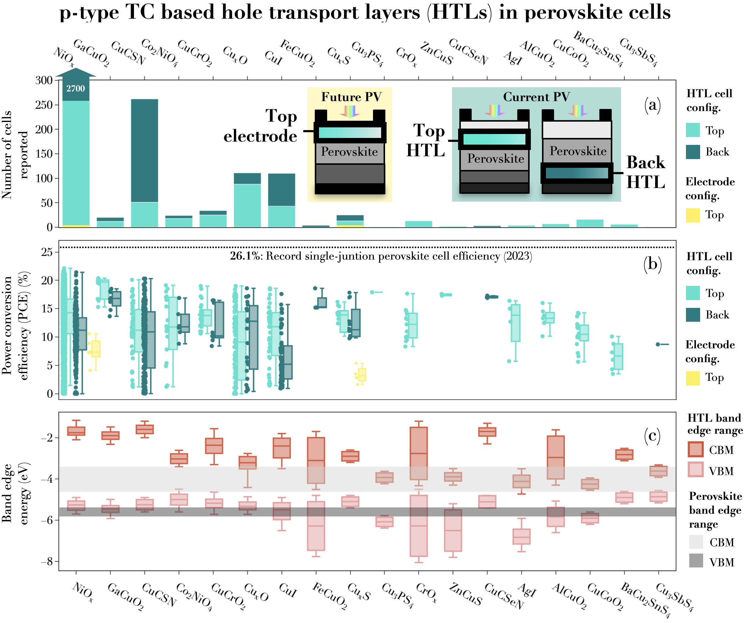
To illustrate the variety of p-type TC contact materials that have been recently incorporated into PV devices, and the magnitude of research efforts as well as what is currently lacking, Figure 6(a) depicts a set of inorganic p-type TCs from the experimental literature which have been implemented as electrodes or HTLs in perovskite solar cell devices (\ceNiO_x is included as a benchmark). Data for this plot has been processed from the open access Perovskite Database.[129] For each reported cell, shading indicates whether it is are part of a double-layer top contact HTL stack, a double-layer back contact HTL stack, or a single-layer top electrode; notably, only two binary materials have been reported as a top electrode, and therefore this is an area for future research. Perovskite cells have been selected here as representative since the search for HTLs is an active area of research and therefore many p-type TCs have recently been attempted; we acknowledge the high hole mobility requirement of p-type TCs is not usually needed for HTLs (and some do not need very high transparency), so this test case represents a specific subset of TC design criteria.
Figure 6(b) plots the distribution or reported power conversion efficiency (PCE) across cells, and materials are sorted by the highest reported PCE for a given material. The highest PCE is from delafossites \ceCuO2 (=Ga, Cr, Fe), spinel \ceNiCo2O4, mixed anion compounds \ceCuCSN and \ceCu3PS4, and binaries \ceCu_xO and \ceCuI (with various doping schemes). We note that none of these p-type TC materials were first predicted computationally; to our knowledge to date no predicted p-type TC has been used as a perovskite HTL. Additionally, these are results from lab-scale cells, not modules; none of the reported materials (except for \ceNiO_x) have been reported in a large-area module.
IV.1 Challenges at interfaces and junctions
Additional complexity emerges at device interfaces, where a TC is in contact with other material layers, which can lead to serious optimization challenges. Before incorporating into a full device, sometimes new contacts are tested on a heterojunction or a “half-cell” to assess the interface and demonstrate rectification properties (stage 6). One of the first challenges to emerge at the interface of a p-type TC and its adjacent layer(s) is interfacial stability. The interface must be stable without reacting, decomposing or segregating into unintentional secondary materials or inducing trap states. For example, although \ceCu_xZn_1-xS is stable as a thin film, growing it as a back contact to CdTe solar cells induces complete decomposition of the \ceCu_xZn_1-xS layer into CdZnS and CuTe.[107] Although \ceNiO_x is commonly used as a HTM for perovskite solar cells, at certain processing conditions it has been shown to react with the perovskite layer and introduce an interfacial defect layer; similarly, \ceNiO_x in contact with Si in a SHJ cell likely introduces an interfacial layer of \ceSiO_x. The Materials Project’s interfacial reaction calculator can be applied as a simple indicator of whether a reaction product is likely to form thermodynamically at an interface and, if so, the degree of instability (whether it will likely passivate or decompose). However even if an interface is thermodynamically stable, it can still degrade over time after operating in non-equilibrium conditions, such as in light-induced degradation (LID). For example, the morphology and doping of n-type top contacts can impact the degree of LID,[130] and, in perovskites, HTMs \ceNiO_x and PEDOT:PSS degrade upon light exposure,[131] but this effect is nontrivial to predict without experiments.
When incorporating a novel p-type layer into a PV device, electronic band edges have to be aligned such that they enable desired junction properties. Ideally, the VBM of the p-type TC should be aligned to the VBM of the layer it extracts holes from. In addition, the CBM of the TC should be sufficiently shallow to form an electron-blocking barrier with the same layer. These criteria are important in particular for hole selective contacts for thin film PV, and for p-type layers in tandems. For example, in CdTe solar cells a rule-of-thumb is that the VBM offset of the p-type contact and CdTe absorber layer should be within 0.3 eV.[132] Figure 6(c) plots literature-reported band offsets for p-type TCs used as HTLs in perovskite solar cells, showing that for most TCs the VBM range is close to the range of various perovskite absorber layers (-5.42 eV to -5.77 eV, referenced to vacuum[133]). However, precise band alignment may not be crucial if the TC is placed next to another highly-doped layer, or if it is a tunneling layer. In SHJ cells it has been shown that if the hole selective contact is not highly doped, its VB has to be aligned very close to that of its neighboring layer (within 0.1 eV) to enable high efficiencies. On the contrary, if the p-type TC layer is highly doped above cm3, high efficiency can be achieved within a wider tolerance to VB misalignment.[43]
A combination of X-ray photoemission spectroscopy (XPS) and first principles slab calculations can be used to assess band offsets of new TCs. Uncertainties of DFT alignments are less than 0.3 eV with LDA and GGA-PBE (this is included as error bars in Figure 6),[134] and this error becomes problematic if a precise degree of alignment is required between layers. Band offsets can differ depending on the surface morphology, including crystallographic plane, surface termination and defects, so there is often a mismatch between computed bulk band offsets and measured offsets in polycrystalline TCs.[135] Band offsets are usually not computed early in TC screenings, but sometimes are assessed in computational deep dives (stage 2). Offsets for an individual material are not sufficient to simulate band bending when in contact with another material, so continuum simulations should be also performed to assess band bending and quasi-Fermi level splitting at a new interface.
In addition to chemical stability and electronic alignment, fabrication of the p-type TC layer must form strong bonds and mechanically adhere to adjacent layers. Mechanical breakage at interfaces can induce detrimental voids or pinholes, which can result in increased electrical resistance and heat losses, and air or moisture gaps can facilitate degradation. These challenges are exacerbated in layered non-isotropic p-type TCs such as delafossite \ceCuAlO2, as highlighted in Figure 5(f) for two \ceCuAlO2-Si heterojunctions,[106] where high contact resistance due to poor adhesion has been a major barrier to scaling solar devices. It is expected this may be the case for predicted layered structures such as \ce[Cu2S2][Ba3Sc2O5].[136]. Some PV applications such as perovskites are moving towards flexible substrates, so designing p-type TCs layers to avoid mechanical breakages will become even more important as these devices come to market.
IV.2 Practical solar cell design
When a solar cell is fabricated using a new contact material (stage 7), cell performance is determined not only by intrinsic material properties but also by interfacial properties, in particular electronic band alignment, and the possible presence of interfacial defects. Surface passivation of contacts and absorbers is in fact an important line of research in thin film and heterojunction-based PV, however, this topic goes beyond the purpose of this review.[137, 138] Defects at interfaces can have different origins, from chemical intermixing to the presence of dangling bonds, among others. However, the role of these defects are rarely considered in early-stage materials design. Therefore, an open challenge is the development of screening metrics to assess interfacial or pinning defects that may arise at contact interfaces, and how they may limit performance. To assess this, it is important to also pre-define the type of absorber material and assess its properties simultaneously. Integrating methods that merge defect calculations and materials predictions with continuum interface simulations in solar cell contact layers could provide valuable insights into the behavior of device-relevant defects under actual operating conditions.[139]
Besides engineering defects, another important consideration for device design is optimizing fabrication method, including designing for temperature stability (most devices have a “thermal budget”). A growth method that works well for synthesizing a single film on a substrate may not be appropriate for a full device stack. In thin film solar cells, contact layers with low thermal budgets of a few hundred degrees C are usually preferable; the process temperature of the TC should not be so high to cause unwanted reactions in the bulk of the absorber or at the interface. However, many of the synthesis recipes for the best reported p-type TCs higher temperatures during some step of the process.[93] For example, Mg-doped \ceCuCrO2 grown by sputtering is one of the highest performing p-type TCs but requires a synthesis temperature of 750 C, which limits its practicality for devices.[3] However, recent developments have enabled low temperature \ceCuCrO2 synthesis and incorporation at an HTL in perovskite cells with high efficiency (see Figure 6).[140] Furthermore, plasma-assisted techniques such as sputtering, pulsed laser deposition (PLD), and plasma-enhanced chemical vapor deposition (PECVD) are often used to deposit TCs, and these methods can be harsh on the underlying material; however, it has recently been shown that oxide TCs can be deposited on perovskites with very low damage by PLD.[141, 142] P-type TC films for PV applications that will operate in the sun also need to be stable under UV irradiation, both in their bulk form and at their interfaces, though this is less important in superstrate devices in which glass absorbs much of the UV. It is also important to consider the lifetime of the device when designing materials to be incorporated, for example whether migration of dopants or segregation into secondary phases will occur over time.
In PV contacts, the tolerance to non-ideal properties such as electronic misalignment depends strongly on device architecture. Tolerances of a TC property within a given device may depend on multiple material and junction properties and therefore may be better described by a multi-objective optimization scheme rather than a serial screening “funnel”. For example, precise band alignment may not be as relevant if the TC is placed next to another highly-doped layer, or if it is a tunneling layer. In SHJ cells it has been shown that if the hole selective contact is not highly doped, its VB has to be aligned very close to that of its neighboring layer (within 0.1 eV) to enable high efficiencies. However, if the p-type TC layer is highly doped above cm3, high efficiency can be achieved within a wider tolerance to VB misalignment.[43] Other properties besides alignment also depend on the device configuration. Perhaps most trivially, the wavelengths to which a material must be transparent depends on the absorption spectrum of the absorber layer. Similarly, the high mobility requirement and threshold varies dramatically across absorber technologies and device designs.
Similar to the novelty bias mentioned previously, one practical challenge when incorporating new materials into solar cell devices is that device architectures are optimized around conventional materials. For example, SHJ solar cells have been highly optimized using a hydrogenated boron-doped amorphous silicon (B-doped p-a-Si:H) and ITO bilayer as the hole-selective top contact, with thicknesses and dopings of these layers and adjacent layers tuned specifically to work well with these materials. Thus, one cannot simply remove a highly optimized material (e.g., a-Si), insert a new layer (e.g., novel p-type TC) into the same device stack, and expect it to deliver optimal properties, even if that new material has high transparency and conductivity. Rather, the entire device may have to be re-optimized to accommodate the new architecture, energetic alignment, and emergent defects from inserting this new layer. However, this can be tedious when working with a large quantity of candidates in high-throughput methods, and thus this is not typically done. As a result a feedback loop ensues: device layers are limited to a small set of materials (that is, small compared to the size of computational databases) that are well-optimized, heavily characterized, easy and cheap to grow, and therefore are more likely to work well in a given device architecture. Then, more resources are invested in further optimizing these already well-optimized materials, and new materials such as predicted p-type TCs have a larger barrier to entry.
IV.3 Scalability and sustainability
To our knowledge, a high-performance solar module using p-type TC contacts has not yet been fabricated. However, if a high-performance p-type TC can someday be successfully integrated into a small-scale laboratory cell, the next stage toward commercialization would involve scaling up to full-sized module devices (stage 9 in Figure 3), which would introduce a new set of challenges. Module performance tends to lag behind cell performance, namely due to the requirement for larger surface area deposition and lower tolerance for non-uniformities.[143] Challenges such as large-area conformity, uniform crystallinity, and strong adhesion without pinholes are exacerbated for thinner films,[144] and since contact layers tend to be thinner than absorber layers in solar cells there is likely less tolerance in contacts for such nonidealities. TC layers in modules also need to be stable for decades and maintain high transparency and electrical conductivity while minimizing resistance losses and avoiding localized performance drops due to defects.
Several deposition methods used regularly to synthesize TCs in lab-based devices are non-uniform by design and challenging to scale, such as spin coating and pulsed laser deposition (PLD), though wafer-scale PLD of ITO, Zr:\ceIn2O3, and SnO2 for perovskites or SHJ cells has recently been demonstrated.[145, 146, 142] Other deposition methods such as sputtering are regularly adapted for large-area deposition, but require re-optimization and often result in performance lower than small cells. ITO is usually deposited by large-area sputtering in SHJ, perovskite, and SHJ-perovskite tandem modules,[147] while in CdTe modules the n-type top contact FTO is usually deposited by CVD and can be done by the glass manufacturer [148]. Several studies have demonstrated large-area fabrication of buffers and contacts such as \ceNiO_x for perovskite module applications,[149] but scaling CuI and other inorganic HTLs while maintaining performance remains an open challenge.[150] Even if physically possible to scale, many high-vacuum synthesis techniques such as MBE are simply too expensive and labor-intensive to use commercially. Developing low-cost, module-scale synthesis techniques such as roll-to-roll printing early on in the p-type TC “design-to-device” development process could enable more rapid integration into next-generation modules. Incorporating economic modeling such as techno-economic analysis can help guide integration of new materials into low-cost devices.[151]
Although the ultimate goal of scaling PV is to mitigate climate change, input and outputs from production and deployment may cause unintentional consequences such damage to ecosystems and human health, and there is an ethical responsibility to minimize harm as we scale new materials such as TCs.[152, 153] Techniques such as life cycle assessment (LCA) can be used to identify key sources of negative impacts within a technology’s life cycle and guide research directions to reduce harm.[154] PV has much lower environmental impacts than fossil fuel technologies due to negligible inputs and outputs during operation, but impacts do emerge from mining, refining, manufacturing, and decommissioning.[155] Mining of critical PV materials can lead to resource depletion, human health impacts, and ecotoxicity, and has motivated shifting towards “earth-abundant” materials,[156] such as moving away from indium in n-type TCs. However, in all PV devices most life cycle GHG emissions are from the energy intensity of material production rather than mining.[157] In conventional PV emissions are primarily from refining solar-grade silicon, but in emerging PV many of these manufacture-stage emissions are also from contact layers. For example, in perovskite tandems, fabrication of contacts and buffers such as Spiro-MeOTAD and sputtered ITO contribute significantly to greenhouse gas (GHG) emissions from the cell.[147] Thin film PV tends to yield lower impacts compared to Si-based PV,[158, 159] which motivates scaling thin film PV with high-performing heterojunction contacts, so designing contact materials with low energy intensity processing could significantly reduce life cycle impacts.
Historically, LCAs are conducted after technologies reach commercial scale, which can lead to “technology lock-in” that makes it challenging to replace harmful materials.[153] While there have been instances of course correction and phase-out — for example, recent efforts to reduce Co-content in \ceLiCoO2-based batteries and the formation of NMC in \ceLiNi_Mn_Co_O2 to address cobalt supply chain hazards (which still rely on lithium and nickel)[160] — some of this lock-in is unavoidable if we want to rapidly deploy renewable energy. One such trade-off is that delaying deployment to wait for PV with lower embodied carbon would result in more emissions than installing existing PV, so it is important that conventional Si (e.g., PERC) is rapidly installed.[161]
Low-TRL emerging PV technologies are years or even decades away from commercialization, but offer serious opportunities for sustainability improvements. These are technologies in which TCs play an important role, so designing new contacts for emerging PV with low environmental impacts could make a big impact. Assessing impacts early in the materials design phase is challenging,[162] particularly when the synthesis route is unknown, and especially for p-type TCs since understanding their underlying physics and design criteria is still lacking. Computational materials discovery often assumes optimization can reduce impacts, e.g., from replacement of elements or reduction of processing energy. For example, a computationally-predicted p-type TC (\ceBeSiP2) has recently been proposed with a new design criteria, forbidden optical transitions; this material contains Be and is impractical to scale, but this design criteria may be applicable to an earth-abundant version that has not yet been discovered,[30] and being too restrictive could lead to missed opportunities. However, we should keep in mind that there is always a certain amount of risk with this approach since later-stage replacements can be difficult. For example, despite significant research efforts, replacing a toxic element in perovskite absorbers (Pb) with a non-toxic element (e.g., Sn, Bi) has not yet yielded high enough performance.[163]
The following question arises: how can materials scientists integrate life cycle thinking throughout the full process of materials discovery and design to prevent “locking-in” technologies with detrimental impacts? This challenge calls for the development of early-stage metrics and strategies for embedding sustainability early in the materials design process. Inspiration can be drawn from recent approaches like emerging materials risk analysis,[164] “upscaling” manufacturing assessments,[165] and the framework of anticipatory LCA.[153, 166] Moreover, we encourage the continued development of new metrics — assessing for embedded carbon, co-product assessment, manufacturing impacts, and end-of-life considerations — that can be incorporated into the design of p-type TCs for emerging PV and sustainable materials discovery in general.
V Insights for future design of p-type TCs
This article has reviewed various disconnects throughout the materials discovery process of p-type TCs, spanning from computational design to material synthesis and from lab-scale devices to scalable sustainable modules. To address these disconnects to design commercially-relevant p-type transparent conductors, we propose the following recommendations for materials designers:
-
1.
Improve and benchmark descriptors for p-type TCs, especially for band gap, dopability, mobility Since the first high-throughput screening for p-type TCOs appeared a decade ago, first principles computational methods have improved tremendously and computing power has increased. More accurate assessment of band gap and mobility are emerging with different levels of accuracy and cost. Assessment of defects and dopability is still among the most expensive computations to perform, but they have been automatized and tractable high-throughput defect approaches are emerging. Predictive low-cost descriptors of dopability have not yet been developed, and including transport properties such as grain boundary scattering at early stages is not common, but both of these pursuits would accelerate screening tremendously. In the last decade available data from which to screen has also grown tremendously, such as in the Materials Project and other large databases, and opportunities to use machine learning to speed up the screening process are naturally emerging from this data.
-
2.
Judiciously assess whether predictions are actually synthesizable. Before lab-based synthesis, higher-accuracy metrics should be used to assess synthesizability of emerging screening candidates. To closer approximate synthesizability of realistic thin film and interface defects, computational screenings should seek better metrics than alone. The ability to move from thermodynamic metrics to assessment of synthesizability in screenings is an important future frontier of computational materials design.
-
3.
Establish standards and consensus on how defect calculations are run and interpreted. There are inconsistencies across the literature in terms of which corrections to use, and qualitative interpretation of formation energies and Fermi level pinning. To avoid inconsistencies and assist comparison across the literature, quantitative assessment of carrier concentration is recommended rather that simply stating whether a material is “dopable.” Following lessons learned from Hu et al.’s quadruple perovskite study about the “importance of reasonable band gap description and chemical boundary determination in predicting defect thermodynamics,”[167] is recommended to standardize running hybrid defect calculations to confirm p-type dopability.
-
4.
Screen for tunability and tolerance ranges, rather than a single compound with a single property. Tuning stoichiometry and doping in the lab can introduce effects not typically considered in bulk calculations, so techniques to simulate tunability would be useful. While very important in practical materials, the effects of alloying and off-stoichiometry are not often not taken into account early on in high-throughput studies, so addressing this gap could lead to new TCs and other material predictions.
-
5.
Be judicious whether metrics and materials are device-appropriate. Searches should be tailored to specific applications, rather than a generic “high-performance” p-type TC. Some properties matter less than others depending on application, and by using generic screenings useful targeted materials may be overlooked. For example, for some devices there may be trade-offs between properties such that achieving optimal performance is a multi-parameter optimization problem (e.g., carrier concentration and band alignment can be coupled). Assessing these trade-offs may require iterative research and learning between stages 1–9 in Figure 3, and synergizing high-throughput computation with multi-scale modeling and device testing.
-
6.
Develop sustainability and scalability metrics to incorporate early in the materials design process. To avoid “locking-in” technologies with detrimental environmental effects, materials scientists should integrate life cycle thinking throughout the design process, drawing inspiration from recent methodologies like emerging materials risk analysis and anticipatory life cycle assessment. Development of early-stage metrics assessing embedded carbon, co-product impacts, manufacturing impacts, and end-of-life aspects could help guide sustainable materials discovery in the field of emerging PV and beyond.
-
7.
Conduct more interdisciplinary analyses to bring computed materials into devices. Historically, separate research teams have performed computations, synthesis, fabrication, and scale-up modeling, which can lead to communication barriers. However, there is a recent trend towards connecting theorists, experimentalists, and analysts on a single project. Ultimately, more communication and collaboration between scientists across various stages of materials discovery can help address these disconnects and lead to more effective design.
The goal of p-type transparent conductor (TC) materials discovery is to predict a new TC from first principles that can scale up and be used in devices such as solar panels for more efficient and sustainable technological development. Although we have made major progress in this field, there is still a large gap between the research stage of proposing a new candidate and actually incorporating the candidate into a device. In this perspective, we have highlighted some major disconnects from the past ten years of research, as well as insights for future design of p-type TCs. We hope that these insights can be applied to future design approaches to catalyze a more rapid and targeted progression in the field of transparent conductors for sustainable energy technologies.
Acknowledgments
This work was supported by the U.S. Department of Energy, Office of Science, Office of Basic Energy Sciences, Materials Sciences and Engineering Division under Contract No. DE-AC02-05-CH11231 (Materials Project program KC23MP). R.W.R. was supported by the U.C. Berkeley Chancellor’s Fellowship and the National Science Foundation (NSF) Graduate Research Fellowship under Grant No. DGE1106400 and DGE175814, and by University of Washington’s Clean Energy Institute. G.H. acknowledges support from the U.S. Department of Energy, Office of Science, Basic Energy Sciences under award number DE-SC0023509. The work of A.C. was supported in part by a research grant (42140) from VILLUM FONDEN and co-funded by the European Union (ERC, IDOL, 101040153). Views and opinions expressed are however those of the authors only and do not necessarily reflect those of the European Union or the European Research Council. Neither the European Union nor the granting authority can be held responsible for them.
VI Author contributions
We highlight the author contributions to this study using the CRediT taxonomy.
R.W.R.: Conceptualization, Methodology, Data Curation, Visualization, Investigation, Writing - Original Draft, Writing – Review & Editing, Funding Acquisition, Project Administration; M.M.M.: Methodology, Investigation, Writing – Review & Editing, Funding Acquisition; G.H.: Methodology, Investigation, Writing – Review & Editing, Funding Acquisition; A.C.: Methodology, Investigation, Writing – Review & Editing, Funding Acquisition;
Supplemental Information
The following supplemental data tables are included, and are available via on the MPContribs platform:
-
•
Computational predictions of p-type TCs
-
•
Experimental reports of predicted p-type TCs
References
- [1] D. S. Ginley and J. D. Perkins, Transparent conductors. Springer, 2011.
- [2] J. Willis and D. O. Scanlon, “Latest directions in p-type transparent conductor design,” Journal of Materials Chemistry C, vol. 9, no. 36, pp. 11995–12009, 2021.
- [3] R. Nagarajan, A. Draeseke, A. Sleight, and J. Tate, “p-type conductivity in cucr 1- x mg x o 2 films and powders,” Journal of Applied Physics, vol. 89, no. 12, pp. 8022–8025, 2001.
- [4] J. Wang, J. Li, and S.-S. Li, “Native p-type transparent conductive cui via intrinsic defects,” Journal of Applied Physics, vol. 110, no. 5, 2011.
- [5] A. E. Delahoy and S. Y. Guo, “Transparent and semitransparent conducting film deposition by reactive-environment, hollow cathode sputtering,” vol. 23, no. 4, pp. 1215–1220.
- [6] A. Jain, S. P. Ong, G. Hautier, W. Chen, W. D. Richards, S. Dacek, S. Cholia, D. Gunter, D. Skinner, G. Ceder, and K. A. Persson, “Commentary: The Materials Project: A materials genome approach to accelerating materials innovation,” vol. 1, no. 1, p. 011002.
- [7] S. Curtarolo, W. Setyawan, S. Wang, J. Xue, K. Yang, R. H. Taylor, L. J. Nelson, G. L. W. Hart, S. Sanvito, M. Buongiorno-Nardelli, N. Mingo, and O. Levy, “AFLOWLIB.ORG: A distributed materials properties repository from high-throughput ab initio calculations,” vol. 58, pp. 227–235.
- [8] S. Kirklin, J. E. Saal, B. Meredig, A. Thompson, J. W. Doak, M. Aykol, S. Rühl, and C. Wolverton, “The open quantum materials database (OQMD): Assessing the accuracy of DFT formation energies,” vol. 1, p. 15010.
- [9] G. Brunin, G.-M. Rignanese, and G. Hautier, “High-performance transparent conducting oxides through small-polaron transport,” Physical Review Materials, vol. 3, no. 6, p. 064602, 2019.
- [10] G. Hautier, A. Miglio, G. Ceder, G.-M. Rignanese, and X. Gonze, “Identification and design principles of low hole effective mass p-type transparent conducting oxides,” vol. 4, p. 2292.
- [11] J. B. Varley, A. Miglio, V. A. Ha, M. J. V. Setten, G. M. Rignanese, and G. Hautier, “High-throughput design of non-oxide p-type transparent conducting materials: Data mining, search strategy, and identification of boron phosphide,” vol. 29, no. 6, pp. 2568–2573.
- [12] R. Woods-Robinson, D. Broberg, A. Faghaninia, A. Jain, S. S. Dwaraknath, and K. A. Persson, “Assessing high-throughput descriptors for prediction of transparent conductors,” Chemistry of Materials, vol. 30, no. 22, pp. 8375–8389, 2018.
- [13] G. Brunin, F. Ricci, V.-A. Ha, G.-M. Rignanese, and G. Hautier, “Transparent conducting materials discovery using high-throughput computing,” npj Computational Materials, vol. 5, no. 1, p. 63, 2019.
- [14] H. Peng, A. Zakutayev, S. Lany, T. R. Paudel, M. d’Avezac, P. F. Ndione, J. D. Perkins, D. S. Ginley, A. R. Nagaraja, N. H. Perry, et al., “Li-doped cr2mno4: a new p-type transparent conducting oxide by computational materials design,” Advanced Functional Materials, vol. 23, no. 42, pp. 5267–5276, 2013.
- [15] A. Bhatia, G. Hautier, T. Nilgianskul, A. Miglio, J. Sun, H. J. Kim, K. H. Kim, S. Chen, G.-M. Rignanese, X. Gonze, and J. Suntivich, “High-mobility bismuth-based transparent p-Type oxide from high-throughput material screening,” vol. 28, no. 1, pp. 30–34.
- [16] N. Sarmadian, R. Saniz, B. Partoens, and D. Lamoen, “Easily doped p-type, low hole effective mass, transparent oxides,” vol. 6, pp. 1–9.
- [17] B. A. D. Williamson, J. Buckeridge, J. Brown, S. Ansbro, R. G. Palgrave, and D. O. Scanlon, “Engineering valence band dispersion for high mobility p-type semiconductors,” vol. 29, no. 6, pp. 2402–2413.
- [18] J. Shi, T. F. Cerqueira, W. Cui, F. Nogueira, S. Botti, and M. A. Marques, “High-throughput search of ternary chalcogenides for p-Type transparent electrodes,” vol. 7, pp. 1–13.
- [19] R. K. M. Raghupathy, T. D. Kühne, C. Felser, and H. Mirhosseini, “Rational design of transparent p-type conducting non-oxide materials from high-throughput calculations,” Journal of Materials Chemistry C, vol. 6, no. 3, pp. 541–549, 2018.
- [20] R. Kormath Madam Raghupathy, H. Wiebeler, T. D. Kuhne, C. Felser, and H. Mirhosseini, “Database screening of ternary chalcogenides for p-type transparent conductors,” Chemistry of Materials, vol. 30, no. 19, pp. 6794–6800, 2018.
- [21] K. Yim, Y. Youn, M. Lee, D. Yoo, J. Lee, S. H. Cho, and S. Han, “Computational discovery of p-type transparent oxide semiconductors using hydrogen descriptor,” npj Computational Materials, vol. 4, no. 1, p. 17, 2018.
- [22] Y. Youn, M. Lee, D. Kim, J. K. Jeong, Y. Kang, and S. Han, “Large-scale computational identification of p-type oxide semiconductors by hierarchical screening,” Chemistry of Materials, vol. 31, no. 15, pp. 5475–5483, 2019.
- [23] V.-A. Ha, G. Yu, F. Ricci, D. Dahliah, M. J. van Setten, M. Giantomassi, G.-M. Rignanese, and G. Hautier, “Computationally driven high-throughput identification of cate and li 3 sb as promising candidates for high-mobility p-type transparent conducting materials,” Physical Review Materials, vol. 3, no. 3, p. 034601, 2019.
- [24] Y. Hu, X. Yao, D. G. Schlom, S. Datta, and K. Cho, “First principles design of high hole mobility p-type sn–o–x ternary oxides: Valence orbital engineering of sn2+ in sn2+–o–x by selection of appropriate elements x,” Chemistry of Materials, vol. 33, no. 1, pp. 212–225, 2020.
- [25] J. Shi, E. A. Rubinstein, W. Li, J. Zhang, Y. Yang, T.-L. Lee, C. Qin, P. Yan, J. L. MacManus-Driscoll, D. O. Scanlon, et al., “Modulation of the bi3+ 6s2 lone pair state in perovskites for high-mobility p-type oxide semiconductors,” Advanced Science, vol. 9, no. 6, p. 2104141, 2022.
- [26] F. Yan, X. Zhang, Y. G. Yu, L. Yu, A. Nagaraja, T. O. Mason, and A. Zunger, “Design and discovery of a novel half-heusler transparent hole conductor made of all-metallic heavy elements,” Nature communications, vol. 6, no. 1, p. 7308, 2015.
- [27] V.-A. Ha, B. Karasulu, R. Maezono, G. Brunin, J. B. Varley, G.-M. Rignanese, B. Monserrat, and G. Hautier, “Boron phosphide as a p-type transparent conductor: Optical absorption and transport through electron-phonon coupling,” Physical Review Materials, vol. 4, no. 6, p. 065401, 2020.
- [28] A. Crovetto, J. M. Adamczyk, R. R. Schnepf, C. L. Perkins, H. Hempel, S. R. Bauers, E. S. Toberer, A. C. Tamboli, T. Unold, and A. Zakutayev, “Boron phosphide films by reactive sputtering: Searching for a p-type transparent conductor,” Advanced Materials Interfaces, vol. 9, no. 12, p. 2200031, 2022.
- [29] M. Barone, M. Foody, Y. Hu, J. Sun, B. Frye, S. S. Perera, B. Subedi, H. Paik, J. Hollin, M. Jeong, et al., “Growth of ta2sno6 films, a candidate wide-band-gap p-type oxide,” The Journal of Physical Chemistry C, vol. 126, no. 7, pp. 3764–3775, 2022.
- [30] R. Woods-Robinson, Y. Xiong, J.-X. Shen, N. Winner, M. K. Horton, M. Asta, A. M. Ganose, G. Hautier, and K. A. Persson, “Designing transparent conductors using forbidden optical transitions,” arXiv preprint arXiv:2303.16994, 2023.
- [31] G. Hautier, A. Miglio, D. Waroquiers, G.-M. Rignanese, and X. Gonze, “How does chemistry influence electron effective mass in oxides? a high-throughput computational analysis,” Chemistry of Materials, vol. 26, no. 19, pp. 5447–5458, 2014.
- [32] A. J. Jackson, B. J. Parrett, J. Willis, A. M. Ganose, W. W. Leung, B. A. Williamson, Y. Liu, T. K. Kim, M. Hoesch, L. S. Veiga, et al., “Computational prediction and experimental realisation of earth abundant transparent conducting oxide ga-doped znsb2o6,” 2022.
- [33] VDMA, “International technology roadmap for photovoltaic (itrpv),” tech. rep., ITRPV, 2023.
- [34] B. J. Stanbery, M. Woodhouse, and J. van de Lagemaat, “Photovoltaic deployment scenarios towards global decarbonization: Role of disruptive technologies,” Solar RRL, 2023.
- [35] D. Dahliah, G. Brunin, J. George, V.-A. Ha, G.-M. Rignanese, and G. Hautier, “High-throughput computational search for high carrier lifetime, defect-tolerant solar absorbers,” Energy & Environmental Science, vol. 14, no. 9, pp. 5057–5073, 2021.
- [36] D. Broberg, K. Bystrom, S. Srivastava, D. Dahliah, B. A. Williamson, L. Weston, D. O. Scanlon, G.-M. Rignanese, S. Dwaraknath, J. Varley, et al., “High-throughput calculations of charged point defect properties with semi-local density functional theory—performance benchmarks for materials screening applications,” npj Computational Materials, vol. 9, no. 1, p. 72, 2023.
- [37] A. N. Fioretti and M. Morales-Masis, “Bridging the p-type transparent conductive materials gap: synthesis approaches for disperse valence band materials,” Journal of Photonics for Energy, vol. 10, no. 4, pp. 042002–042002, 2020.
- [38] T. Minemoto, T. Matsui, H. Takakura, Y. Hamakawa, T. Negami, Y. Hashimoto, T. Uenoyama, and M. Kitagawa, “Theoretical analysis of the effect of conduction band offset of window/cis layers on performance of cis solar cells using device simulation,” Solar Energy Materials and Solar Cells, vol. 67, no. 1-4, pp. 83–88, 2001.
- [39] N. R. E. Laboratory, “Best Research-Cell Efficiency Chart,” 2023.
- [40] N. R. E. Laboratory, “Champion Photovoltaic Module Efficiency Chart,” 2023.
- [41] X. Zhang, L. Zhang, J. D. Perkins, and A. Zunger, “Intrinsic transparent conductors without doping,” Physical review letters, vol. 115, no. 17, p. 176602, 2015.
- [42] K. Lejaeghere, S. Cottenier, and V. Van Speybroeck, “Ranking the stars: A refined pareto approach to computational materials design,” Physical Review Letters, vol. 111, no. 7, p. 075501, 2013.
- [43] R. Woods-Robinson, V. Stevanović, S. Lany, K. N. Heinselman, M. K. Horton, K. A. Persson, and A. Zakutayev, “Role of disorder in the synthesis of metastable zinc zirconium nitrides,” Physical Review Materials, vol. 6, no. 4, p. 043804, 2022.
- [44] R. Gautier, X. Zhang, L. Hu, L. Yu, Y. Lin, T. O. Sunde, D. Chon, K. R. Poeppelmeier, and A. Zunger, “Prediction and accelerated laboratory discovery of previously unknown 18-electron abx compounds,” Nature chemistry, vol. 7, no. 4, pp. 308–316, 2015.
- [45] J. Xu, J.-B. Liu, J. Wang, B.-X. Liu, and B. Huang, “Prediction of novel p-type transparent conductors in layered double perovskites: A first-principles study,” Advanced Functional Materials, vol. 28, no. 26, p. 1800332, 2018.
- [46] W. Sun, S. T. Dacek, S. P. Ong, G. Hautier, A. Jain, W. D. Richards, A. C. Gamst, K. A. Persson, and G. Ceder, “The thermodynamic scale of inorganic crystalline metastability,” Science advances, vol. 2, no. 11, p. e1600225, 2016.
- [47] M. Aykol, S. S. Dwaraknath, W. Sun, and K. A. Persson, “Thermodynamic limit for synthesis of metastable inorganic materials,” Science advances, vol. 4, no. 4, p. eaaq0148, 2018.
- [48] V. I. Hegde, M. Aykol, S. Kirklin, and C. Wolverton, “The phase stability network of all inorganic materials,” Science advances, vol. 6, no. 9, p. eaay5606, 2020.
- [49] C. J. Bartel, S. L. Millican, A. M. Deml, J. R. Rumptz, W. Tumas, A. W. Weimer, S. Lany, V. Stevanović, C. B. Musgrave, and A. M. Holder, “Physical descriptor for the gibbs energy of inorganic crystalline solids and temperature-dependent materials chemistry,” Nature communications, vol. 9, no. 1, p. 4168, 2018.
- [50] V. Stevanović, “Sampling polymorphs of ionic solids using random superlattices,” vol. 116, no. 7, p. 075503.
- [51] S. Haastrup, M. Strange, M. Pandey, T. Deilmann, P. S. Schmidt, N. F. Hinsche, M. N. Gjerding, D. Torelli, P. M. Larsen, A. C. Riis-Jensen, et al., “The computational 2d materials database: high-throughput modeling and discovery of atomically thin crystals,” 2D Materials, vol. 5, no. 4, p. 042002, 2018.
- [52] M. Aykol, J. H. Montoya, and J. Hummelshøj, “Rational solid-state synthesis routes for inorganic materials,” Journal of the American Chemical Society, 2021.
- [53] N. Szymanski, Y. Zeng, H. Huo, C. Bartel, H. Kim, and G. Ceder, “Toward autonomous design and synthesis of novel inorganic materials,” Materials Horizons, 2021.
- [54] A. Davariashtiyani, Z. Kadkhodaie, and S. Kadkhodaei, “Predicting synthesizability of crystalline materials via deep learning,” Communications Materials, vol. 2, no. 1, p. 115, 2021.
- [55] H. Huo, C. J. Bartel, T. He, A. Trewartha, A. Dunn, B. Ouyang, A. Jain, and G. Ceder, “Machine-learning rationalization and prediction of solid-state synthesis conditions,” Chemistry of Materials, vol. 34, no. 16, pp. 7323–7336, 2022.
- [56] N. J. Szymanski, B. Rendy, Y. Fei, R. E. Kumar, T. He, D. Milsted, M. J. McDermott, M. Gallant, E. D. Cubuk, A. Merchant, et al., “An autonomous laboratory for the accelerated synthesis of novel materials,” Nature, pp. 1–6, 2023.
- [57] J. Montoya, C. Grimley, M. Aykol, C. Ophus, H. Sternlicht, B. H. Savitzky, A. M. Minor, S. Torrisi, J. Goedjen, C.-C. Chung, et al., “Computer-assisted discovery and rational synthesis of ternary oxides,” 2023.
- [58] M. J. McDermott, S. S. Dwaraknath, and K. A. Persson, “A graph-based network for predicting chemical reaction pathways in solid-state materials synthesis,” Nature communications, vol. 12, no. 1, p. 3097, 2021.
- [59] M. J. McDermott, B. C. McBride, C. E. Regier, G. T. Tran, Y. Chen, A. A. Corrao, M. C. Gallant, G. E. Kamm, C. J. Bartel, K. W. Chapman, et al., “Assessing thermodynamic selectivity of solid-state reactions for the predictive synthesis of inorganic materials,” ACS Central Science, 2023.
- [60] C. Toher, C. Oses, D. Hicks, and S. Curtarolo, “Unavoidable disorder and entropy in multi-component systems,” Npj Computational Materials, vol. 5, no. 1, p. 69, 2019.
- [61] A. Walsh and J.-S. Park, “The holey grail of transparent electronics,” Matter, vol. 3, no. 3, pp. 604–606, 2020.
- [62] H. Kawazoe, M. Yasukawa, H. Hyodo, M. Kurita, H. Yanagi, and H. Hosono, “P-type electrical conduction in transparent thin films of cualo2,” Nature, vol. 389, no. 6654, pp. 939–942, 1997.
- [63] K. Ahn, G. H. Kim, S.-J. Kim, J. Kim, G.-S. Ryu, P. Lee, B. Ryu, J. Y. Cho, Y.-H. Kim, J. Kang, et al., “Highly conductive p-type transparent conducting electrode with sulfur-doped copper iodide,” Chemistry of Materials, vol. 34, no. 23, pp. 10517–10527, 2022.
- [64] F. Geng, Y.-N. Wu, D. Splith, L. Wang, X. Kang, X. Chen, P. Guo, S. Liang, L. Yang, M. Lorenz, et al., “Amorphous transparent cu (s, i) thin films with very high hole conductivity,” The Journal of Physical Chemistry Letters, vol. 14, no. 26, pp. 6163–6169, 2023.
- [65] A. S. Mirza, M. Pols, W. Soltanpoor, S. Tao, G. Brocks, and M. Morales-Masis, “The role of sulfur in sulfur-doped copper (i) iodide p-type transparent conductors,” Matter, 2023.
- [66] M. Kumar, A. Dubey, N. Adhikari, S. Venkatesan, and Q. Qiao, “Strategic review of secondary phases, defects and defect-complexes in kesterite czts–se solar cells,” Energy & Environmental Science, vol. 8, no. 11, pp. 3134–3159, 2015.
- [67] L. Y. Liang, Z. M. Liu, H. T. Cao, Y. Y. Shi, X. L. Sun, Z. Yu, A. H. Chen, H. Z. Zhang, and Y. Q. Fang, “Improvement of phase stability and accurate determination of optical constants of sno thin films by using al2o3 capping layer,” ACS applied materials & interfaces, vol. 2, no. 6, pp. 1565–1568, 2010.
- [68] J.-H. Cha and D.-Y. Jung, “Air-stable transparent silver iodide–copper iodide heterojunction diode,” ACS applied materials & interfaces, vol. 9, no. 50, pp. 43807–43813, 2017.
- [69] A. Crovetto, H. Hempel, M. Rusu, L. Choubrac, D. Kojda, K. Habicht, and T. Unold, “Water adsorption enhances electrical conductivity in transparent p-type cui,” ACS Applied Materials & Interfaces, vol. 12, no. 43, pp. 48741–48747, 2020.
- [70] A. K. Singh, L. Zhou, A. Shinde, S. K. Suram, J. H. Montoya, D. Winston, J. M. Gregoire, and K. A. Persson, “Electrochemical stability of metastable materials,” Chemistry of Materials, vol. 29, no. 23, pp. 10159–10167, 2017.
- [71] N. M. Twyman, A. Walsh, and T. Buonassisi, “Environmental stability of crystals: a greedy screening,” Chemistry of Materials, vol. 34, no. 6, pp. 2545–2552, 2022.
- [72] J. Willis, I. Bravić, R. R. Schnepf, K. N. Heinselman, B. Monserrat, T. Unold, A. Zakutayev, D. O. Scanlon, and A. Crovetto, “Prediction and realisation of high mobility and degenerate p-type conductivity in cacup thin films,” Chemical Science, vol. 13, no. 20, pp. 5872–5883, 2022.
- [73] R. Cao, H.-X. Deng, and J.-W. Luo, “Design principles of p-type transparent conductive materials,” ACS applied materials & interfaces, vol. 11, no. 28, pp. 24837–24849, 2019.
- [74] M. Chan and G. Ceder, “Efficient band gap prediction for solids,” Phys. Rev. Letters, vol. 105, no. 19, p. 196403, 2010.
- [75] M. Van Setten, M. Giantomassi, X. Gonze, G.-M. Rignanese, and G. Hautier, “Automation methodologies and large-scale validation for g w: Towards high-throughput g w calculations,” Physical Review B, vol. 96, no. 15, p. 155207, 2017.
- [76] C. Chen, Y. Zuo, W. Ye, X. Li, and S. P. Ong, “Learning properties of ordered and disordered materials from multi-fidelity data,” Nature Computational Science, vol. 1, no. 1, pp. 46–53, 2021.
- [77] Z. Yuan, D. Dahliah, M. R. Hasan, G. Kassa, A. Pike, S. Quadir, R. Claes, C. Chandler, Y. Xiong, V. Kyveryga, et al., “Discovery of the zintl-phosphide bacd {} p {} as a long carrier lifetime and stable solar absorber,” arXiv preprint arXiv:2310.18188, 2023.
- [78] A. Walsh, J. L. Da Silva, S.-H. Wei, C. Körber, A. Klein, L. Piper, A. DeMasi, K. E. Smith, G. Panaccione, P. Torelli, et al., “Nature of the band gap of \ceIn2O3 revealed by first-principles calculations and x-ray spectroscopy,” Physical Review Letters, vol. 100, no. 16, p. 167402, 2008.
- [79] M. Baranowski, P. Plochocka, R. Su, L. Legrand, T. Barisien, F. Bernardot, Q. Xiong, C. Testelin, and M. Chamarro, “Exciton binding energy and effective mass of cspbcl 3: a magneto-optical study,” Photonics Research, vol. 8, no. 10, pp. A50–A55, 2020.
- [80] J.-J. Zhou, J. Park, I.-T. Lu, I. Maliyov, X. Tong, and M. Bernardi, “Perturbo: A software package for ab initio electron–phonon interactions, charge transport and ultrafast dynamics,” Computer Physics Communications, vol. 264, p. 107970, 2021.
- [81] H. Lee, S. Poncé, K. Bushick, S. Hajinazar, J. Lafuente-Bartolome, J. Leveillee, C. Lian, F. Macheda, H. Paudyal, W. H. Sio, et al., “Electron-phonon physics from first principles using the epw code,” arXiv preprint arXiv:2302.08085, 2023.
- [82] G. Brunin, H. P. C. Miranda, M. Giantomassi, M. Royo, M. Stengel, M. J. Verstraete, X. Gonze, G.-M. Rignanese, and G. Hautier, “Phonon-limited electron mobility in si, gaas, and gap with exact treatment of dynamical quadrupoles,” Physical Review B, vol. 102, no. 9, p. 094308, 2020.
- [83] R. Claes, G. Brunin, M. Giantomassi, G.-M. Rignanese, and G. Hautier, “Assessing the quality of relaxation-time approximations with fully automated computations of phonon-limited mobilities,” Physical Review B, vol. 106, no. 9, p. 094302, 2022.
- [84] A. M. Ganose, J. Park, A. Faghaninia, R. Woods-Robinson, K. A. Persson, and A. Jain, “Efficient calculation of carrier scattering rates from first principles,” Nature communications, vol. 12, no. 1, p. 2222, 2021.
- [85] J. Willis, R. Claes, Q. Zhou, M. Giantomassi, G.-M. Rignanese, G. Hautier, and D. O. Scanlon, “Limits to hole mobility and doping in copper iodide,” 2023.
- [86] D. Broberg, B. Medasani, N. E. Zimmermann, G. Yu, A. Canning, M. Haranczyk, M. Asta, and G. Hautier, “Pycdt: A python toolkit for modeling point defects in semiconductors and insulators,” Computer Physics Communications, vol. 226, pp. 165–179, 2018.
- [87] A. Goyal, P. Gorai, H. Peng, S. Lany, and V. Stevanović, “A computational framework for automation of point defect calculations,” Computational Materials Science, vol. 130, pp. 1–9, 2017.
- [88] Y. Xiong, C. Bourgois, N. Sheremetyeva, W. Chen, D. Dahliah, H. Song, J. Zheng, S. M. Griffin, A. Sipahigil, and G. Hautier, “High-throughput identification of spin-photon interfaces in silicon,” Science Advances, vol. 9, no. 40, p. eadh8617, 2023.
- [89] J. Thomas, W. Chen, Y. Xiong, B. Barker, J. Zhou, W. Chen, A. Rossi, N. Kelly, Z. Yu, D. Zhou, et al., “A substitutional quantum defect in ws2 discovered by high-throughput computational screening and fabricated by site-selective stm manipulation,” 2023.
- [90] I. Mosquera-Lois, S. R. Kavanagh, A. Walsh, and D. O. Scanlon, “Identifying the ground state structures of point defects in solids,” npj Computational Materials, vol. 9, no. 1, p. 25, 2023.
- [91] Y. Kumagai, “Computational screening of p-type transparent conducting oxides using the optical absorption spectra and oxygen-vacancy formation energies,” Physical Review Applied, vol. 19, no. 3, p. 034063, 2023.
- [92] R. X. Yang, C. A. McCandler, O. Andriuc, M. Siron, R. Woods-Robinson, M. K. Horton, and K. A. Persson, “Big data in a nano world: a review on computational, data-driven design of nanomaterials structures, properties, and synthesis,” ACS nano, vol. 16, no. 12, pp. 19873–19891, 2022.
- [93] M. Morales-Masis, S. De Wolf, R. Woods-Robinson, J. W. Ager, and C. Ballif, “Transparent electrodes for efficient optoelectronics,” Advanced Electronic Materials, vol. 3, no. 5, p. 1600529, 2017.
- [94] D. Joshi and R. Srivastava, “Mobility and carrier concentration in polycrystalline silicon,” Solar Cells, vol. 12, no. 3, pp. 337–344, 1984.
- [95] K. Ellmer, D. Ginley, H. Hosono, and D. Paine, “Handbook of transparent conductors,” Transparent Conductive Zinc Oxide and Its Derivatives, pp. 193–263, 2010.
- [96] H. Marom, M. Ritterband, and M. Eizenberg, “The contribution of grain boundary scattering versus surface scattering to the resistivity of thin polycrystalline films,” Thin Solid Films, vol. 510, no. 1-2, pp. 62–67, 2006.
- [97] K. Ellmer and R. Mientus, “Carrier transport in polycrystalline ito and zno: Al ii: The influence of grain barriers and boundaries,” Thin Solid Films, vol. 516, no. 17, pp. 5829–5835, 2008.
- [98] X. Wang, A. M. Ganose, S. R. Kavanagh, and A. Walsh, “Band versus polaron: Charge transport in antimony chalcogenides,” ACS Energy Letters, vol. 7, no. 9, pp. 2954–2960, 2022.
- [99] J.-H. Pöhls, S. Chanakian, J. Park, A. M. Ganose, A. Dunn, N. Friesen, A. Bhattacharya, B. Hogan, S. Bux, A. Jain, et al., “Experimental validation of high thermoelectric performance in recuznp 2 predicted by high-throughput dft calculations,” Materials Horizons, vol. 8, no. 1, pp. 209–215, 2021.
- [100] G. Jellison Jr, M. Chisholm, and S. Gorbatkin, “Optical functions of chemical vapor deposited thin-film silicon determined by spectroscopic ellipsometry,” Applied physics letters, vol. 62, no. 25, pp. 3348–3350, 1993.
- [101] N. Yamada, R. Ino, and Y. Ninomiya, “Truly transparent p-type -cui thin films with high hole mobility,” Chemistry of Materials, vol. 28, no. 14, pp. 4971–4981, 2016.
- [102] L. Fanni, B. Aebersold, D. Alexander, L. Ding, M. M. Masis, S. Nicolay, and C. Ballif, “c-texture versus a-texture low pressure metalorganic chemical vapor deposition zno films: Lower resistivity despite smaller grain size,” Thin Solid Films, vol. 565, pp. 1–6, 2014.
- [103] S. Kralj, P. Dally, P. Bampoulis, B. Vishal, S. De Wolf, and M. Morales-Masis, “Impact of the tco microstructure on the electronic properties of carbazole-based self-assembled monolayers,” ACS Materials Letters, vol. 6, pp. 366–374, 2023.
- [104] Y. Hu, J. Hwang, Y. Lee, P. Conlin, D. G. Schlom, S. Datta, and K. Cho, “First principles calculations of intrinsic mobilities in tin-based oxide semiconductors sno, sno2, and ta2sno6,” Journal of Applied Physics, vol. 126, no. 18, 2019.
- [105] D. Dahliah, G.-M. Rignanese, and G. Hautier, “Defect compensation in the p-type transparent oxide ba 2 bitao 6,” Journal of Materials Chemistry C, vol. 8, no. 27, pp. 9352–9357, 2020.
- [106] R. A. Ismail, F. F. Rashid, and M. S. Tariq, “Preparation and characteristics study of cualo 2/si heterojunction photodetector by pulsed laser deposition,” Journal of Materials Science: Materials in Electronics, vol. 28, pp. 6889–6896, 2017.
- [107] R. Woods-Robinson, T. Ablekim, A. Norman, S. Johnston, K. A. Persson, M. O. Reese, W. K. Metzger, and A. Zakutayev, “Sputtered p-type cu x zn1–x s back contact to cdte solar cells,” ACS Applied Energy Materials, vol. 3, no. 6, pp. 5427–5438, 2020.
- [108] D. Saranin, P. Gostischev, D. Tatarinov, I. Ermanova, V. Mazov, D. Muratov, A. Tameev, D. Kuznetsov, S. Didenko, and A. Di Carlo, “Copper iodide interlayer for improved charge extraction and stability of inverted perovskite solar cells,” Materials, vol. 12, no. 9, p. 1406, 2019.
- [109] R. Mehta and S. Vogel, “Sputtered cadmium oxide and indium oxide/tin oxide films as transparent electrodes to cadmium sulfide,” Journal of the Electrochemical Society, vol. 119, no. 6, p. 752, 1972.
- [110] I. Rauf, “Structure and properties of tin-doped indium oxide thin films prepared by reactive electron-beam evaporation with a zone-confining arrangement,” Journal of applied physics, vol. 79, no. 8, pp. 4057–4065, 1996.
- [111] J. Robertson and Z. Zhang, “Doping limits in p-type oxide semiconductors,” MRS Bulletin, pp. 1–7, 2021.
- [112] P. Storm, S. Gierth, S. Selle, M. Bar, H. von Wenckstern, M. Grundmann, and M. Lorenz, “Evidence for oxygen being a dominant shallow acceptor in p-type cui,” APL Materials, vol. 9, no. 5, 2021.
- [113] K. R. Talley, J. Mangum, C. L. Perkins, R. Woods-Robinson, A. Mehta, B. P. Gorman, G. L. Brennecka, and A. Zakutayev, “Synthesis of lanthanum tungsten oxynitride perovskite thin films,” Advanced Electronic Materials, vol. 5, no. 7, p. 1900214, 2019.
- [114] F. V. Hensling, D. Dahliah, P. Dulal, P. Singleton, J. Sun, J. Schubert, H. Paik, I. Subedi, B. Subedi, G.-M. Rignanese, et al., “Epitaxial stannate pyrochlore thin films: Limitations of cation stoichiometry and electron doping,” APL Materials, vol. 9, no. 5, 2021.
- [115] G. Frank and H. Köstlin, “Electrical properties and defect model of tin-doped indium oxide layers,” Applied Physics A, vol. 27, pp. 197–206, 1982.
- [116] A. Crovetto, T. S. Ottsen, E. Stamate, D. Kjær, J. Schou, and O. Hansen, “On performance limitations and property correlations of al-doped zno deposited by radio-frequency sputtering,” Journal of Physics D: Applied Physics, vol. 49, no. 29, p. 295101, 2016.
- [117] R. Woods-Robinson, M. K. Horton, and K. A. Persson, “A method to computationally screen for tunable properties of crystalline alloys,” arXiv preprint arXiv:2206.10715, 2022.
- [118] L. Chen, J. Yang, S. Klaus, L. J. Lee, R. Woods-Robinson, J. Ma, Y. Lum, J. K. Cooper, F. M. Toma, L.-W. Wang, et al., “p-type transparent conducting oxide/n-type semiconductor heterojunctions for efficient and stable solar water oxidation,” Journal of the American Chemical Society, vol. 137, no. 30, pp. 9595–9603, 2015.
- [119] G. J. Exarhos, C. F. Windisch Jr, K. F. Ferris, and R. R. Owings, “Cation defects and conductivity in transparent oxides,” Applied Physics A, vol. 89, no. 1, pp. 9–18, 2007.
- [120] Y. Hu, D. Schlom, S. Datta, and K. Cho, “Amorphous ta2sno6: A hole-dopable p-type oxide,” Applied Surface Science, vol. 613, p. 155981, 2023.
- [121] L. A. Mittmann and A. Crovetto, “Phosphosulfide semiconductors for optoelectronics and solar energy conversion,” Jan. 2024.
- [122] P. J. McGinn, “Thin-Film Processing Routes for Combinatorial Materials Investigations—A Review,” ACS Combinatorial Science, vol. 21, pp. 501–515, July 2019.
- [123] K. R. Talley, S. L. Millican, J. Mangum, S. Siol, C. B. Musgrave, B. Gorman, A. M. Holder, A. Zakutayev, and G. L. Brennecka, “Implications of heterostructural alloying for enhanced piezoelectric performance of (Al,Sc)N,” Physical Review Materials, vol. 2, p. 063802, June 2018.
- [124] C. T. Parzyck, C. A. Pennington, W. J. I. DeBenedetti, J. Balajka, E. Echeverria, H. Paik, L. Moreschini, B. D. Faeth, C. Hu, J. K. Nangoi, V. Anil, T. A. Arias, M. A. Hines, D. G. Schlom, A. Galdi, K. M. Shen, and J. M. Maxson, “Atomically smooth films of CsSb: A chemically robust visible light photocathode,” APL Materials, vol. 11, p. 101125, Oct. 2023.
- [125] R. R. Schnepf, A. Crovetto, P. Gorai, A. Park, M. Holtz, K. N. Heinselman, S. R. Bauers, M. Brooks Tellekamp, A. Zakutayev, A. L. Greenaway, E. S. Toberer, and A. C. Tamboli, “Reactive phosphine combinatorial co-sputtering of cation disordered ZnGeP 2 films,” Journal of Materials Chemistry C, vol. 10, no. 3, pp. 870–879, 2022.
- [126] D. P. Tabor, L. M. Roch, S. K. Saikin, C. Kreisbeck, D. Sheberla, J. H. Montoya, S. Dwaraknath, M. Aykol, C. Ortiz, H. Tribukait, et al., “Accelerating the discovery of materials for clean energy in the era of smart automation,” Nature reviews materials, vol. 3, no. 5, pp. 5–20, 2018.
- [127] S. Moradi, S. Kundu, and M. I. Saidaminov, “High-throughput synthesis of thin films for the discovery of energy materials: a perspective,” ACS Materials Au, vol. 2, no. 5, pp. 516–524, 2022.
- [128] S. Fan and Y. Chen, “The electronic structures and p-type performance of group ia and va atoms in nio: A first principles study,” Journal of Applied Physics, vol. 131, no. 13, 2022.
- [129] T. J. Jacobsson, A. Hultqvist, A. García-Fernández, A. Anand, A. Al-Ashouri, A. Hagfeldt, A. Crovetto, A. Abate, A. G. Ricciardulli, A. Vijayan, et al., “An open-access database and analysis tool for perovskite solar cells based on the fair data principles,” Nature Energy, vol. 7, no. 1, pp. 107–115, 2022.
- [130] F. Hamelmann, J. Weicht, and G. Behrens, “Light-induced degradation of thin film silicon solar cells,” in Journal of Physics: Conference Series, vol. 682, p. 012002, IOP Publishing, 2016.
- [131] M. Elnaggar, A. G. Boldyreva, M. Elshobaki, S. A. Tsarev, Y. S. Fedotov, O. R. Yamilova, S. I. Bredikhin, K. J. Stevenson, S. M. Aldoshin, and P. A. Troshin, “Decoupling contributions of charge-transport interlayers to light-induced degradation of p-i-n perovskite solar cells,” Solar RRL, vol. 4, no. 9, p. 2000191, 2020.
- [132] G. K. Liyanage, A. B. Phillips, F. K. Alfadhili, R. J. Ellingson, and M. J. Heben, “The role of back buffer layers and absorber properties for> 25% efficient cdte solar cells,” ACS Applied Energy Materials, vol. 2, no. 8, pp. 5419–5426, 2019.
- [133] A. Jafar, Fabrication and Characterization of Perovskite Solar Cells. PhD thesis, 01 2017.
- [134] S. De Waele, K. Lejaeghere, M. Sluydts, and S. Cottenier, “Error estimates for density-functional theory predictions of surface energy and work function,” Physical Review B, vol. 94, no. 23, p. 235418, 2016.
- [135] K. T. Butler, G. Sai Gautam, and P. Canepa, “Designing interfaces in energy materials applications with first-principles calculations,” npj Computational Materials, vol. 5, no. 1, p. 19, 2019.
- [136] B. A. Williamson, G. J. Limburn, G. W. Watson, G. Hyett, and D. O. Scanlon, “Computationally driven discovery of layered quinary oxychalcogenides: Potential p-type transparent conductors?,” Matter, vol. 3, no. 3, pp. 759–781, 2020.
- [137] P. M. Salome, B. Vermang, R. Ribeiro-Andrade, J. P. Teixeira, J. M. Cunha, M. J. Mendes, S. Haque, J. Borme, H. Aguas, E. Fortunato, et al., “Passivation of interfaces in thin film solar cells: Understanding the effects of a nanostructured rear point contact layer,” Advanced Materials Interfaces, vol. 5, no. 2, p. 1701101, 2018.
- [138] E. Aydin, M. De Bastiani, and S. De Wolf, “Defect and contact passivation for perovskite solar cells,” Advanced Materials, vol. 31, no. 25, p. 1900428, 2019.
- [139] M. D. Jones, J. A. Dawson, S. Campbell, V. Barrioz, L. D. Whalley, and Y. Qu, “Modelling interfaces in thin-film photovoltaic devices,” Frontiers in Chemistry, vol. 10, p. 920676, 2022.
- [140] B. Yang, D. Ouyang, Z. Huang, X. Ren, H. Zhang, and W. C. Choy, “Multifunctional synthesis approach of in: Cucro2 nanoparticles for hole transport layer in high-performance perovskite solar cells,” Advanced Functional Materials, vol. 29, no. 34, p. 1902600, 2019.
- [141] Y. Smirnov, L. Schmengler, R. Kuik, P.-A. Repecaud, M. Najafi, D. Zhang, M. Theelen, E. Aydin, S. Veenstra, S. De Wolf, et al., “Scalable pulsed laser deposition of transparent rear electrode for perovskite solar cells,” Advanced Materials Technologies, vol. 6, no. 2, p. 2000856, 2021.
- [142] W. Soltanpoor, A. E. Bracesco, N. Rodkey, M. Creatore, and M. Morales-Masis, “Low damage scalable pulsed laser deposition of sno2 for p–i–n perovskite solar cells,” Solar RRL, vol. 7, no. 23, p. 2300616, 2023.
- [143] T. D. Lee and A. U. Ebong, “A review of thin film solar cell technologies and challenges,” Renewable and Sustainable Energy Reviews, vol. 70, pp. 1286–1297, 2017.
- [144] S. Abbott, “Practical coatings: pinholes.” https://www.stevenabbott.co.uk/practical-coatings/pinholes.php, 2023. Accessed on: 2023-12-14.
- [145] Y. Smirnov, P.-A. Repecaud, L. Tutsch, I. Florea, K. P. Zanoni, A. Paliwal, H. J. Bolink, P. R. i Cabarrocas, M. Bivour, and M. Morales-Masis, “Wafer-scale pulsed laser deposition of ito for solar cells: reduced damage vs. interfacial resistance,” Materials Advances, vol. 3, no. 8, pp. 3469–3478, 2022.
- [146] K. P. Zanoni, A. Paliwal, M. A. Hernández-Fenollosa, P.-A. Repecaud, M. Morales-Masis, and H. J. Bolink, “Ito top-electrodes via industrial-scale pld for efficient buffer-layer-free semitransparent perovskite solar cells,” Advanced Materials Technologies, vol. 7, no. 10, p. 2101747, 2022.
- [147] M. Roffeis, S. Kirner, J.-C. Goldschmidt, B. Stannowski, L. M. Perez, C. Case, and M. Finkbeiner, “New insights into the environmental performance of perovskite-on-silicon tandem solar cells–a life cycle assessment of industrially manufactured modules,” Sustainable Energy & Fuels, vol. 6, no. 12, pp. 2924–2940, 2022.
- [148] M. A. Scarpulla, B. McCandless, A. B. Phillips, Y. Yan, M. J. Heben, C. Wolden, G. Xiong, W. K. Metzger, D. Mao, D. Krasikov, et al., “Cdte-based thin film photovoltaics: Recent advances, current challenges and future prospects,” Solar Energy Materials and Solar Cells, vol. 255, p. 112289, 2023.
- [149] G. Li, Y. Jiang, S. Deng, A. Tam, P. Xu, M. Wong, and H.-S. Kwok, “Overcoming the limitations of sputtered nickel oxide for high-efficiency and large-area perovskite solar cells,” Advanced Science, vol. 4, no. 12, p. 1700463, 2017.
- [150] A. Liu, H. Zhu, M.-G. Kim, J. Kim, and Y.-Y. Noh, “Engineering copper iodide (cui) for multifunctional p-type transparent semiconductors and conductors,” Advanced Science, vol. 8, no. 14, p. 2100546, 2021.
- [151] L. A. Zafoschnig, S. Nold, and J. C. Goldschmidt, “The race for lowest costs of electricity production: techno-economic analysis of silicon, perovskite and tandem solar cells,” IEEE Journal of Photovoltaics, vol. 10, no. 6, pp. 1632–1641, 2020.
- [152] R. Owen, J. Stilgoe, P. Macnaghten, M. Gorman, E. Fisher, and D. Guston, “A framework for responsible innovation,” Responsible innovation: managing the responsible emergence of science and innovation in society, pp. 27–50, 2013.
- [153] B. A. Wender, R. W. Foley, T. A. Hottle, J. Sadowski, V. Prado-Lopez, D. A. Eisenberg, L. Laurin, and T. P. Seager, “Anticipatory life-cycle assessment for responsible research and innovation,” Journal of Responsible Innovation, vol. 1, no. 2, pp. 200–207, 2014.
- [154] D. W. Pennington, J. Potting, G. Finnveden, E. Lindeijer, O. Jolliet, T. Rydberg, and G. Rebitzer, “Life cycle assessment part 2: Current impact assessment practice,” Environment international, vol. 30, no. 5, pp. 721–739, 2004.
- [155] NREL, “Life cycle greenhouse gas emissions from electricity generation: update,” tech. rep., NREL, 2021.
- [156] J. D. Bergesen, G. A. Heath, T. Gibon, and S. Suh, “Thin-film photovoltaic power generation offers decreasing greenhouse gas emissions and increasing environmental co-benefits in the long term,” Environmental science & technology, vol. 48, no. 16, pp. 9834–9843, 2014.
- [157] “Energy Technology Perspectives 2023,” tech. rep., International Energy Agency (IEA), 2023.
- [158] V. Fthenakis, “Sustainability of photovoltaics: The case for thin-film solar cells,” Renewable and Sustainable Energy Reviews, vol. 13, no. 9, pp. 2746–2750, 2009.
- [159] A. Rashedi and T. Khanam, “Life cycle assessment of most widely adopted solar photovoltaic energy technologies by mid-point and end-point indicators of recipe method,” Environmental Science and Pollution Research, vol. 27, no. 23, pp. 29075–29090, 2020.
- [160] S. Lee and A. Manthiram, “Can cobalt be eliminated from lithium-ion batteries?,” ACS Energy Letters, vol. 7, no. 9, pp. 3058–3063, 2022.
- [161] S. Husein, R. Woods-Robinson, and R. Saive, “Delayed pv deployment negates co2 benefits of ultra-low carbon pv modules,” 2021 IEEE 48th Photovoltaic Specialists Conference (PVSC), 2021.
- [162] V. L. Putsche, J. Pattany, T. Ghosh, S. Atnoorkar, J. Zuboy, A. Carpenter, E. S. Takeuchi, A. C. Marschilok, K. J. Takeuchi, A. Burrell, et al., “A framework for integrating supply chain, environmental, and social justice factors during early stationary battery research,” Frontiers in Sustainability, vol. 4, p. 1287423, 2023.
- [163] W. Ke and M. G. Kanatzidis, “Prospects for low-toxicity lead-free perovskite solar cells,” Nature communications, vol. 10, no. 1, p. 965, 2019.
- [164] M. D. Horgan, H. A. Hsain, J. L. Jones, and K. D. Grieger, “Development and application of screening-level risk analysis for emerging materials,” Sustainable Materials and Technologies, vol. 35, p. e00524, 2023.
- [165] S. Weyand, K. Kawajiri, C. Mortan, and L. Schebek, “Scheme for generating upscaling scenarios of emerging functional materials based energy technologies in prospective lca (upfunmatlca),” Journal of Industrial Ecology, 2023.
- [166] B. A. Wender, R. W. Foley, V. Prado-Lopez, D. Ravikumar, D. A. Eisenberg, T. A. Hottle, J. Sadowski, W. P. Flanagan, A. Fisher, L. Laurin, et al., “Illustrating anticipatory life cycle assessment for emerging photovoltaic technologies,” 2014.
- [167] S. Hu, B. Xia, Y.-P. Lin, T. Katase, J. Fujioka, T. Kamiya, H. Hosono, K.-Z. Du, and Z. Xiao, “p-type transparent quadruple perovskite halide conductors: fact or fiction?,” Advanced Functional Materials, vol. 30, no. 31, p. 1909906, 2020.