A scalable cavity-based spin-photon interface in a photonic integrated circuit
††journal: opticajournal††articletype: Research ArticleA central challenge in quantum networking is transferring quantum states between different physical modalities, such as between flying photonic qubits and stationary quantum memories. One implementation entails using spin-photon interfaces that combine solid-state spin qubits, such as color centers in diamond, with photonic nanostructures. However, while high-fidelity spin-photon interactions have been demonstrated on isolated devices, building practical quantum repeaters requires scaling to large numbers of interfaces yet to be realized. Here, we demonstrate integration of nanophotonic cavities containing tin-vacancy (SnV) centers in a photonic integrated circuit (PIC). Out of a six-channel quantum micro-chiplet (QMC), we find four coupled SnV-cavity devices with an average Purcell factor of 7. Based on system analyses and numerical simulations, we find with near-term improvements this multiplexed architecture can enable high-fidelity quantum state transfer, paving the way towards building large-scale quantum repeaters.
1 Introduction
A principal goal in quantum information science is efficiently distributing entanglement over large distances by transferring quantum states between different physical modalities, such as stationary atomic systems and propagating optical fields. Recent advances in spin-photon interfaces based on color centers in diamond have enabled multi-modality entanglement distribution demonstrations, such as foundational quantum entanglement tests [1] and construction of a multi-node quantum network [2]. In particular, the Group-IV centers are promising candidates due to their optical coherence even when placed in nanostructures [3, 4, 5, 6, 7], high Debye-Waller factors [8], and long spin coherence times [9, 5]. These aforementioned attributes enable demonstrations of high-fidelity quantum state transfer between spins and photons [10] and a multi-qubit repeater node with error detection [11]. The tin-vacancy (SnV) center in the Group-IV family especially has garnered a surging interest due to its large spin-orbital splitting [12, 8], which suppresses phonon-induced decoherence and permits quantum operations at temperatures above 1 K [5], as opposed to the silicon-vacancy centers that require sub-Kelvin temperatures to attain millisecond coherence times [9]. Further photonics engineering around SnV centers has also led to production of highly indistinguishable single photons out of nanophotonic waveguides [6] and coherent coupling to photonic crystal cavities [13, 14].
However, the outstanding challenge towards useful quantum repeaters lies in scaling to spin-photon interfaces to counteract latency and consequently memory decoherence [15, 16, 17, 18, 19, 20], motivating the integration of color centers with photonic integrated circuits (PICs). This hybrid approach [21, 22, 23, 24, 25] leverages foundry-scale manufacturing for essential quantum control functions, including quantum emitter strain tuning [4, 26], spin ground state control [27], and in-situ optical routing and addressing [4, 28]. While coupling quantum emitters to nanocavities has enabled excellent spin-photon cooperativity in single and isolated devices [29], realizing cavity-enhanced interfaces has thus far remained an open challenge in scalable hybrid quantum PIC approaches.
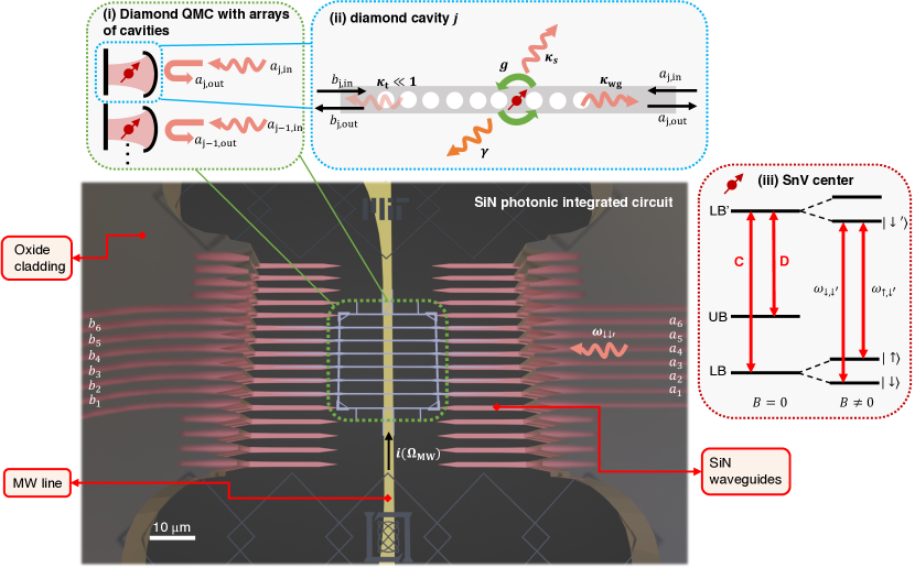
Here, we address this challenge by introducing SnV centers that are coupled to integrated diamond cavities in a quantum microchiplet (QMC). Figure 1 shows a hybrid architecture that integrates a diamond QMC with a silicon nitride (SiN) PIC for optical and electrical addressing of the individual color centers. The oxide-cladded photonic chip contains an oxide opening, in which individual low-loss nitride waveguide evanescently couples to each diamond QMC channel. Each channel includes a diamond nanophotonic cavity coupled to input-output waveguide mode . In our study, we first demonstrate Purcell enhancement of four cavity-coupled SnV systems out of a 6-channel QMC with an average Purcell factor of 7. Second, we heterogeneously integrate a separate cavity QMC into a SiN PIC and perform spectroscopy enabled by on-chip coupling. Based on numerical analyses, this quantum PIC indicates that near-term improvements in cavity-PIC coupling can enable multiplexed quantum repeaters for high-fidelity quantum state transfer.
2 Diamond nanophotonic cavities
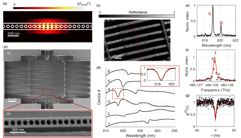
Critical to engineering strong emitter-cavity interaction is maximizing the ratio of cavity quality factor to mode volume [32]. Hence, we design a diamond 1D photonic crystal (PhC) [33, 34, 29, 13, 35] cavity based on a Gaussian chirp (see Supplement 1, Sec. 1). The fundamental TE-like mode achieves simulated and , with mode profile depicted in Fig. 2(a). Using the quasi-isotropic etching technique for undercutting diamond devices [36, 34, 37], we fabricate diamond QMCs containing arrays of 1D PhC cavities (see Supplement 1, Sec. 1). Figure 2(b) illustrates representative devices with a measured geometry defined by the width nm, the thickness nm, and the hole radius nm. To characterize the devices, we excite the cavities’ modes normal to the plane of the sample (marked in Fig. 2(c)) with a pulsed broadband laser and collect its cross-polarized reflection confocally [38]. Due to undercoupling between the cavity and the waveguide modes, i.e. , we find top collection of the scattered photons into free-space enables easier characterization of the cavities’ spectral responses. Figure 2(d) shows examples of cavity reflection spectra acquired at room temperature, with QMC channels 2-6 exhibiting Fano resonances [39] close to 619 nm. We fit these modes to a weighted Fano-Lorentz function [40] (see Supplement 1, Sec. 2). An example fit to channel 4’s resonance is shown in the inset of Fig. 2(d), giving a fitted resonance wavelength nm and . We notice that the cavity improves by a factor of 2.4 as we cool the sample down to 4 K. We attribute the rest of the discrepancy from the simulated to scattering loss due thickness non-uniformity as observed for the underside in Fig. 2(b)(ii), which stems from quasi-isotropic etching [37], as well as surface roughness (see Supplement 1, Sec. 1).
3 Coherent cavity coupling of quantum emitters
To investigate coherent emitter-cavity coupling, we perform spectroscopy of SnV centers in the same QMC as shown in Fig. 2(c) at 4 K. Figure 2(e) shows the photoluminescence spectrum of a SnV center in channel 4 excited off-resonantly at 515 nm. We observe both the C and D transitions at near 619 nm separated by its ground state spin-orbital splitting of 820 GHz. To probe its optical coherence, we perform photoluminescence excitation (PLE) spectroscopy, in which we sweep a narrowband (linewidth kHz) tunable laser across the C transition. Figure 2(f) shows the collected phonon sideband (PSB) fluorescence. We find the fitted Lorentzian center and linewidth to be THz and MHz, which indicates optical dephasing that broadens the linewidth by a factor of 7 of the transform limit defined by its off-resonance lifetime (see Supplement 1, Sec. 8).
Subsequently, we perform an autocorrelation measurement with a Hanbury-Brown-Twiss setup by resonantly exciting the SnV center. Figure 2(g) shows a histogram of correlated photon counts, with plotted against the time delay . We fit the data to the model , where ns is a convolved time scale between the emitter’s lifetime and the resonantly-driven Rabi oscillation rate [41]. The fitted dip at gives , below the classical limit of , affirming the presence of a single SnV center as opposed to an ensemble. Accounting for a 550 ps timing jitter of the detector (based on fit in Fig. 3), we extract the emitter’s PSB signal to be cps against a background of cps [41], which agrees with our measured detector dark counts. With background subtraction, we deduce , limited by the detector jitter.
To ensure coupling between the SnV centers and the PhC cavity modes, we apply in-situ gas tuning with argon [42, 29, 13] to overlap the cavity resonance with the SnV center’s zero-phonon line (ZPL) (see Supplement 1, Sec. 4). We resonantly excite the SnV centers with 500 ps-long pulses generated by an electro-optical modulator (see Supplement 1, Sec. 3). We verify emitter-cavity coupling by measuring the lifetime of SnV centers in each QMC channel.
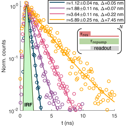
Figure 3 shows lifetime versus emitter-cavity detuning of a SnV center in cavity 6 in the QMC, with ZPL at 619.22 nm. Each lifetime curve is fitted with a single exponential convolved with a Gaussian that represents the instrument response function (IRF) [43] mainly set by the detector’s timing resolution. At large detuning, i.e. nm, the measured lifetime is ns. As decreases, the lifetime monotonically decreases. At close to zero detuning, i.e. nm, the lifetime is shortened to ns. The observed lifetime reduction signifies Purcell enhancement of the SnV center’s spontaneous emission rate due to coherent emitter-cavity coupling [32].
In order to estimate the maximum Purcell factor realized in experiments, we account for the modified local density of states when placing a SnV center in nanostructure and its non-radiative decay pathways out of the excited state by using the definition [44, 42]
| (1) |
where is a product of the SnV center’s quantum efficiency [12, 45] and the Debye-Waller factor [46]. and are the (nearly-)on-resonant and off-resonant lifetimes. We also measure ns typical of what is observed for SnV centers residing in bulk diamond. The estimated Purcell factor for the measured SnV center in Fig. 3 is . Furthermore, we estimate the probability of the SnV center emitting into the cavity mode in the Purcell regime () to be .
| Channel | ZPL (nm) | Purcell Factor | (nm) | ||
|---|---|---|---|---|---|
| 2 | 619.2821 | 4.130.59 | 0.810.16 | 3.120.19 | 613.9 |
| 4 | 619.2560 | 10.401.06 | 0.910.13 | 6.280.32 | 614.4 |
| 5 | 619.2965 | 5.320.72 | 0.840.16 | 3.650.23 | 615.1 |
| 6 | 619.2220 | 8.070.89 | 0.890.14 | 5.250.28 | 611.8 |
Importantly, we achieve multi-channel Purcell enhancement within a single QMC. We find four coupled emitter-cavity systems in channels 2, 4, 5 and 6 (channels 1 and 3 do not contain SnV centers within the cavities). Table 1 shows a summary of each coupled emitter-cavity system’s Purcell factor , -factor, and lifetime reduction ratios . On average, the Purcell factors and -factors acquired from this single QMC are and , respectively.
In particular, one emitter-cavity coupled system in channel 4 exhibits ten-fold Purcell enhancement at . Its cavity factor at close to resonance nm is (see Supplement 1, Sec. 4). Accounting for detuning that reduces the measured Purcell factor by a factor of [44, 47], we estimate the maximum experimental Purcell factor at improves slightly to . The theoretical maximum Purcell factor is (assuming the simulated mode volume). Accounting for dipole misalignment (angular difference between the [111] and [100] crystal axes) reduces the maximum Purcell factor to . We attribute the difference between the theoretical and experimental maxima of a factor of to the SnV center being spatially off-centered from the cavity field maximum, an issue which can be resolved by employing focused ion beam implantation [48] or masked implantation [49] in future efforts.
4 Heterogeneous integration into a PIC
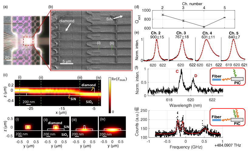
To showcase hybrid integration with diamond color centers, we transfer-print a separate diamond QMC that is more preferentially waveguide-coupled (different from Fig. 2(c)) into a silicon nitride PIC using a PDMS stamp (see Supplement 1, Sec. 6). The PIC supports independent low-loss waveguides coupled to all QMC channels with oxide-cladding designed for optimal edge-coupling with single-mode fibers [50, 51]. Identical to what is depicted in Fig. 1, Fig. 4(a) is a microscope image of the oxide opening, with white lines defining its boundaries. In dark field imaging, the ground and MW lines appear as the purple regions (with tessellated patterns on top). Extending into the oxide opening "socket" from both left and right sides are parallel SiN waveguides, on top of which we transfer-print the QMC [52, 53]. Figure 4(b) shows a SEM image of the socket containing the integrated QMC. Due to a pitch mismatch between the QMC and the SiN waveguides, only channels 2-5 are optically coupled for measurements. We estimate roughly a 21 m overlap in length between diamond and SiN waveguides, both of which are adiabatically tapered to minimize scattering loss. With the diamond (SiN) waveguide tapering down from 260 nm (1 m) to 50 nm (0 nm) in width over 9 m (4 m) in length, the transmission efficiency is simulated to be at 619 nm in FDTD at zero angular offset. Based on the SEM, we estimate an alignment angular offset of degree with a corresponding transmission efficiency (see Supplement 1, Sec. 6). Figure 4(c) shows the propagating TE mode out of the cavity from the diamond waveguide (left) to the evanescently coupled SiN waveguide (right) on oxide, with mode profiles evaluated at four selected points: (i) suspended diamond waveguide before overlapping with SiN, (ii) in the overlapped region at 10 m and (iii) at 2.25 m from the diamond tip, and (iv) SiN waveguide on oxide. The SiN waveguide mode for each channel is then routed to an inversely tapered waveguide at the chip’s edge for optimal optical coupling to a single-mode fiber [51].
Next, we perform cavity transmission measurements at room temperature. The efficient coupling between the diamond and SiN waveguides enables observation of cavity resonances by top excitation of the cavity mode and collection from an edge-coupled fiber. Figure 4(d) displays the statistics of the measured factors based on the Fano resonance spectra shown in Fig. 4(e). The fitted are 90015, 76718, 63111, 8407, respectively.
Furthermore, optical coupling between the diamond QMC and the PIC enables us to perform spectroscopy on SnV centers at 1.3 K. By exciting at the cavity center of channel 2 off-resonantly at 515 nm, we observe again C and D transitions of an ensemble of SnV centers as shown in Fig. 4(f). We also perform PLE spectroscopy via resonant excitation to selectively probe individual SnV centers. Figure 4(g) shows a PLE curve indicating the presence of three peaks, which could indicate either the presence of multiple emitters or nuclear-electro hyperfine transitions from the Sn-117 isotope (see Supplement 1, Sec. 10) [54]. The fitted ZPL positions are 484.0904 THz, 484.0906 THz, and 484.0912 THz, with linewidths MHz, MHz, MHz, respectively. The smallest observed linewidth is a factor of from the observed transform limit 27.8 MHz (based on the average detuned lifetime of the 4 devices studied in Table 1). Preservation of optical coherence of SnV centers showcases the suitability of the integrated QMC-PIC platform as an efficient spin-photon interface.
5 Projected state transfer fidelity and success probability
The compactness of the PIC allows parallel addressing of multiple channels in the QMC, crucial for memory multiplexing that boosts the quantum state transfer rate between photonic and spin qubits. Importantly, optical routing in a miniaturized PIC provides intrinsic phase stability necessary for high-fidelity interference-based operations [55]. In particular, we consider a cavity reflection-based protocol in which a polarization-encoded photonic qubit acquires a spin-state-dependent phase and is detected to herald photon-to-spin state transfer [30, 56, 55] (see Supplement 1, Sec. 11).
In this protocol, the fidelity hinges on the cavity reflection coefficient (see Supplement 1, Sec. 11) as a function of pure dephasing , the emitter-cavity coupling strength , and diamond waveguide-cavity coupling . is the cavity mode’s decay rate into the waveguide and is its total decay rate, where is the scattering loss rate, as shown in Fig. 1. Based on the cavity-enhancement results (Fig. 2(f) and channel 4 in Fig. 3(b)), we estimate pure dephasing MHz and emitter-cavity coupling GHz (see Supplement 1, Sec. 11). The investigated diamond cavities are designed to maximize and are consequently undercoupled to the diamond waveguide mode. Based on FDTD simulations, the coupling strength is calculated to be .
Next, to estimate the success probability of state transferring, we extract the relevant efficiencies by considering optical losses from the cavity center to the detector. Specifically, we analyze the three subsystems: (i) the device consisting of the diamond QMC and the SiN PIC, (ii) the fiber setup, and (iii) the free-space optics setup (see Supplement 1, Sec. 7). For (i), we account for waveguide-cavity coupling , transmission efficiency from diamond waveguide to the SiN waveguide in the uncladded socket (0.91 based on FDTD), directional coupler (0.5), transmission through the junction where uncladded and oxide-cladded regions meet (0.53 [51]), propagation in the PIC (0.99 [50]), and fiber edge-coupling efficiency (0.3 measured at 620 nm, see Supplement 1, Sec. 6). The estimated efficiency is . For (ii), given the measured fiber transmission from inside the cryostat to the external setup (0.61) and fiber insertion efficiency (conservative estimate of 0.89 per fiber-to-fiber connection), the estimated efficiency is . Lastly, for (iii), the free-space setup’s efficiency is . Prior to detection, the overall collection efficiency is . Assuming a detector’s efficiency of 0.65, the overall detection efficiency is then , primarily limited by the waveguide-cavity coupling strength .
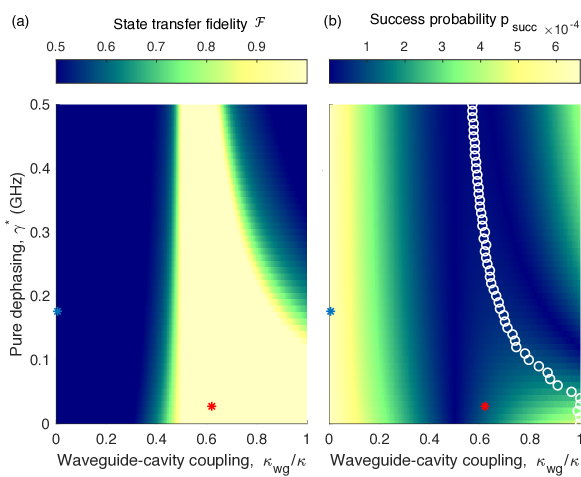
Using our current device performance and treating the waveguide-cavity coupling as a variable, we estimate the fidelity and success probability that this quantum PIC platform could achieve for quantum state transfer, a key operation for quantum networking. Crucially, the protocol we consider is based on the Duan-Kimble scheme [30] that relies on spin-state-dependent cavity reflection, in particular the polarization mode reflects off the bare cavity whereas the polarization mode acquires a phase from the spin coupled to a TE-mode cavity. We first extract an overall detection efficiency and excitation efficiencies and without accounting for . The success probability is then defined as , where is the cavity reflection coefficient dependent on both the frequency and the waveguide-cavity coupling strength (see Supplement 1 Section 11. Sweeping over both and , Fig. 5(a,b) indicate a trade-off between and when pure dephasing is present.
For pure dephasing less than 0.5 MHz, increases sharply close to the critical coupling regime . Intuitively, in the undercoupling regime , the phase contrast between and is much less than (see Supplement 1, Sec. 11), hence limiting the spin-photon entanglement fidelity. As increases past , increases to unity and eventually rolls off with finite pure dephasing. The point at which is maximized by an optimal choice of is marked as a white circle in Fig. 5(b) for each value of .
Based on the PLE curve shown in Fig. 2(f), in which the total measured linewidth is where is the transform-limit, we estimate pure dephasing to be MHz. Our current waveguide-cavity coupling is estimated to be , which leads to a fidelity at the classical limit , as shown by the blue marker in Fig. 5(a). Next, we project how and vary with better optical coherence and improvements on the photonic cavity design. For the former, we use the narrowest linewidth out of the peaks displayed in Fig. 4(g) with a corresponding pure dephasing of MHz. As for the latter, we take state-of-the-art waveguide-cavity coupling of demonstrated in Ref. [35]. Our calculation shows that the fidelity can improve to with , as shown by the red star markers in Fig. 5(a,b).
Clearly, to boost both state transfer fidelity and success probability hinge critically on improving the waveguide-cavity coupling strength. As stated previously, our current device is only designed to maximize . One approach to better the photonic crystal cavity design is to adiabatically reduce the mirror strength of the waveguide-coupled side, entailing tapering down the air hole size and decreasing the number of holes [35]. Another alternative is to utilize the “sawfish“ photonic crystal cavity, which has no air holes but instead modulated waveguide width, a feature which is conducive to improve out-coupling to the adjacent waveguide [55, 57].
To further enhance success probability without trading off fidelity demands improving the total collection efficiency. First, the large scattering loss present at the oxide junction can be reduced to dB by employing inter-layer SiN waveguide coupling [58]. Second, instead of using a fiber array with standard optical fiber, lensed fibers can be used to better mode matching and consequently the edge coupling efficiency. Additionally, using a detector with higher quantum efficiency, e.g. superconducting nanowire single-photon detectors, can boost the detection efficiency to 99 [10]. As a result, the overall detection efficiency without considering diamond waveguide-cavity coupling can improve to 0.19, about an order of magnitude higher than the current value.
Relatedly, improving various components contributing to the total collection efficiency is not only important for state transfer success probability, but also imperative for maintaining the SnV center’s charge state during coherent quantum operations. Our current PLE and lifetime measurements require 515 nm illumination to stabilize the negatively-charged SnV centers [59]. As Ref. [7] has shown, however, this need to apply aboveband light can be avoided by applying nW resonant laser power, which requires a high excitation/detection efficiency and may be within reach with the aforementioned ameliorating measures.
Lastly, reduction in pure dephasing also leads to eliminating the trade-off between fidelity and success probability, as shown by Fig. 5(a,b). Although near-transform-limited linewidth has been observed in the SnV centers in the PIC-integrated QMC shown in Fig. 4(g), there still remains defect centers exhibiting much worse optical dephasing such as the one presented in Fig. 2(f). We suspect the variance in linewidths stems from the emitters’ proximity to the sidewalls, which could introduce surface charge noises [60]. Modifying the cavity design that reduce proximity to sidewalls [61, 57] could then potentially lower on top of benefiting waveguide-cavity coupling. Additional materials engineering may also be necessitated. Low-energy ion implantation to minimize lattice damage has been shown to improve optical coherence [62]. Studies of high-pressure and high-temperature (HPHT) treatment [12, 46] have also demonstrated narrowing of the inhomogeneous distribution of defect centers’ emissions in diamond. This could suggest HPHT heals the diamond lattice from implantation damage, and may minimize pure dephasing caused by nearby vacancy defects. Our current diamond samples have been implanted at relatively high dosage of ions/cm2. Future studies with lower implantation energy and subsequent HPHT treatment can potentially reduce pure dephasing due to defects formed from lattice damage.
6 Outlook and conclusions
In this work, we experimentally realize a multi-channel cavity-enhanced spin-photon interface in a single diamond QMC [4]. We show yield in demonstrating SnV-cavity coupling in four out of six channels, with an average Purcell factor of 7. We further demonstrate heterogeneous integration of diamond emitter-cavity systems into a SiN PIC. The photonic chip optically interposes to edge-coupled fibers that enable on-chip characterization of nanocavities with exceeding and emitter spectroscopy unveiling an optical linewidth MHz close to the transform limit at 1.3 K. Based on the experimental results, we extract the relevant system parameters and simulate the photon-to-spin state transfer fidelity and success probability [30, 56, 55]. Our findings suggest that this hybrid architecture can achieve spin-photon state transfer fidelity nearing unity and success probability exceeding for building near-term quantum network nodes by considering improvements on several key components.
This work should motivate future efforts to use chip-integrated spin-cavity systems to perform multiplexed spin-photon entanglement and teleportation. This entails utilizing microwave lines to coherently control individual spin qubits [63] and integrating single photon detectors for more efficient optical measurements [64, 65]. The integration approach can also be applied to active PIC platforms not covered in this work, such as aluminum nitride [66, 67, 4, 68], gallium phosphide [69, 70], lithium niobate [71, 72], and silicon carbide [73, 74], all of which permit high-bandwidth switching networks for high entanglement generation rates, where memory multiplexing eliminates the effect of memory saturation [15, 16, 17, 18, 75, 20, 76]. The discussed physics and engineering platform extend beyond the use of color centers in diamond. Other promising solid-state qubits such as quantum dots [77, 78, 79], color centers in silicon carbide [73], rare-earth ions [80, 81], and defects in silicon [82, 83, 84, 85] can benefit as well from the many functionalities bestowed by integrated photonics. Lastly, directional couplers form phase-stable on-chip interferometers for entangling spin-cavities between different local channels, allowing building cluster states crucial for measurement-based quantum computation [86] and error-corrected quantum communication [87].
7 Backmatter
Funding
Acknowledgments We thank Isaac Harris, Eric Bersin, and Madison Sutula for insightful discussions. K.C.C. acknowledges funding support by the National Science Foundation (NSF) RAISE-TAQS 1839155 and the MITRE Corporation Moonshot program. I.C. acknowledges support from the National Defense Science and Engineering Graduate (NDSEG) Fellowship Program, the NSF EFRI ACQUIRE program EFMA-1641064 and NSF award DMR-1747426. H.R. acknowledges support from the NDSEG Fellowship Program and the NSF Center for Ultracold Atoms (CUA) No. 1734011. L.D. acknowledge funding from the European Union’s Horizon 2020 research and innovation program under the Marie Sklodowska-Curie grant agreement No. 840393. L.L. acknowledges funding from NSF QISE-NET award DMR-1747426 and the ARO MURI W911NF2110325. M.T. performed this work, in part, with funding from the Center for Integrated Nanotechnologies, an Office of Science User Facility operated for the US Department of Energy Office of Science. D.E. acknowledges funding support from the NSF RAISE TAQS program 1839155, the NSF Engineering Research Center for Quantum Networks (CQN), awarded under cooperative agreement number 1941583, and the NSF C-ACCEL program.
Disclosures Distribution Statement A. Approved for public release. Distribution is unlimited. This material is based upon work supported by the National Reconnaissance Office and the Under Secretary of Defense for Research and Engineering under Air Force Contract No. FA8702-15-D-0001. Any opinions, findings, conclusions or recommendations expressed in this material are those of the authors and do not necessarily reflect the views of the National Reconnaissance Office or the Under Secretary of Defense for Research and Engineering. 2023 Massachusetts Institute of Technology. Delivered to the U.S. Government with Unlimited Rights, as defined in DFARS Part 252.227-7013 or 7014 (Feb 2014). Notwithstanding any copyright notice, U.S. Government rights in this work are defined by DFARS 252.227-7013 or DFARS 252.227-7014 as detailed above. Use of this work other than as specifically authorized by the U.S. Government may violate any copyrights that exist in this work.
D.E. holds shares in Quantum Network Technologies; these interests have been disclosed to MIT and reviewed in accordance with its conflict of interest policies, with any conflicts of interest to be managed accordingly.
Data Availability Statement All relevant experimental data are available within the Article and its Supplementary Information. Numerical simulation data are available on request from authors.
Supplemental document See Supplement 1 for supporting content.
References
- [1] H. Bernien, B. Hensen, W. Pfaff, et al., “Heralded entanglement between solid-state qubits separated by three metres,” \JournalTitleNature 497, pp.86–90 (2013).
- [2] M. Pompili, S. L. N. Hermans, S. Baier, et al., “Realization of a multinode quantum network of remote solid-state qubits,” \JournalTitleScience 372, pp.259–264 (2021).
- [3] R. E. Evans, A. Sipahigil, D. D. Sukachev, et al., “Narrow-linewidth homogeneous optical emitters in diamond nanostructures via silicon ion implantation,” \JournalTitlePhys. Rev. Applied 5, 044010 (2016).
- [4] N. H. Wan, T.-J. Lu, K. C. Chen, et al., “Large-scale integration of near-indistinguishable artificial atoms in hybrid photonic circuits,” \JournalTitleNature 583, pp.226–231 (2020).
- [5] R. Debroux, C. P. Michaels, C. M. Purser, et al., “Quantum control of the tin-vacancy spin qubit in diamond,” \JournalTitlePhys. Rev. X 11, 041041 (2021).
- [6] J. A. Martinez, R. A. Parker, K. C. Chen, et al., “Photonic indistinguishability of the tin-vacancy center in nanostructured diamond,” \JournalTitlePhys. Rev. Lett. 129, 173603 (2022).
- [7] R. A. Parker, J. A. Martinez, K. C. Chen, et al., “A diamond nanophotonic interface with an optically accessible deterministic electronuclear spin register,” \JournalTitleNat. Photonics (2023).
- [8] G. Thiering and A. Gali, “Ab initio magneto-optical spectrum of group-iv vacancy color centers in diamond,” \JournalTitlePhys. Rev. X 8, 021063 (2018).
- [9] D. D. Sukachev, A. Sipahigil, C. T. Nguyen, et al., “Silicon-vacancy spin qubit in diamond: a quantum memory exceeding 10 ms with single-shot state readout,” \JournalTitlePhys. Rev. Lett. 119, 223602 (2017).
- [10] M. K. Bhaskar, R. Riedinger, B. Machielse, et al., “Experimental demonstration of memory-enhanced quantum communication,” \JournalTitleNature 580, pp.60–64 (2020).
- [11] P. Stas, Y. Q. Huan, B. Machielse, et al., “Robust multi-qubit quantum network node with integrated error detection,” \JournalTitleScience 378, pp.557–560 (2022).
- [12] T. Iwasaki, Y. Miyamoto, T. Taniguchi, et al., “Tin-vacancy quantum emitters in diamond,” \JournalTitlePhys. Rev. Lett. 119, 253601 (2017).
- [13] A. E. Rugar, S. Aghaeimeibodi, D. Riedel, et al., “Quantum photonic interface for tin-vacancy centers in diamond,” \JournalTitlePhys. Rev. X 11, 031021 (2021).
- [14] K. Kuruma, B. Pingault, C. Chia, et al., “Coupling of a single tin-vacancy center to a photonic crystal cavity in diamond,” \JournalTitleAppl. Phys. Lett. 118, 230601 (2021).
- [15] S. B. van Dam, P. C. Humphreys, F. Rozpedek, et al., “Multiplexed entanglement generation over quantum networks using multi-qubit nodes,” \JournalTitleQuantum Sci. Technol. 2, 034002 (2017).
- [16] E. Shchukin, F. Schmidt, and P. van Loock, “Waiting time in quantum repeaters with probabilistic entanglement swapping,” \JournalTitlePhys. Rev. A 100, 032322 (2019).
- [17] Y. Lee, E. Bersin, A. Dahlberg, et al., “A quantum router architecture for high-fidelity entanglement flows in quantum networks,” \JournalTitlenpj Quant. Info. 8, 75 (2020).
- [18] W. Dai and D. Towsley, “Entanglement swapping for repeater chains with finite memory sizes,” \JournalTitlearXiv p. 2111.10994 (2021).
- [19] P. Dhara, A. Patil, H. Krovi, and S. Guha, “Subexponential rate versus distance with time-multiplexed quantum repeaters,” \JournalTitlePhys. Rev. A 104, 052612 (2021).
- [20] H. Choi, M. G. Davis, A. G. Inesta, and D. R. Englund, “Scalable quantum networks: congestion-free hierarchical entanglement routing with error correction,” \JournalTitlearXiv p. 2306.09216 (2023).
- [21] O. Benson, “Assembly of hybrid photonic architectures from nanophotonic constituents,” \JournalTitleNature 480, pp.193–199 (2011).
- [22] M. Davanco, J. Liu, L. Sapienza, et al., “Heterogeneous integration for on-chip quantum photonic circuits with single quantum dot devices,” \JournalTitleNat. Commun. 8, 889 (2017).
- [23] A. W. Elshaari, W. Pernice, K. Srinivasan, et al., “Hybrid integrated quantum photonic circuits,” \JournalTitleNat. Photon. 14, pp.285–298 (2020).
- [24] J.-H. Kim, S. Aghaeimeibodi, J. Carolan, et al., “Hybrid integration methods for on-chip quantum photonics,” \JournalTitleOptica 7, pp.291–308 (2020).
- [25] G. Moody, V. J. Sorger, D. J. Blumenthal, et al., “2022 roadmap on integrated quantum photonics,” \JournalTitleJ. Phys. Photonics 4, 012501 (2022).
- [26] G. Clark, H. Raniwala, M. Koppa, et al., “Nanoelectromechanical control of spin-photon interfaces in a hybrid quantum system on chip,” \JournalTitleNano Lett. 24, 4, pp.1316–1323 (2023).
- [27] D. A. Golter, G. Clark, T. E. Dandachi, et al., “Selective and scalable control of spin quantum memories in a photonic circuit,” \JournalTitleNano Lett. 23, 17, pp.7852–7858 (2023).
- [28] K. J. Palm, M. Dong, D. A. Golter, et al., “Modular chip-integrated photonic control of artificial atoms in diamond waveguides,” \JournalTitleOptica 10, 634–641 (2023).
- [29] C. T. Nguyen, D. D. Sukachev, M. K. Bhaskar, et al., “Quantum network nodes based on diamond qubits with an efficient nanophotonic interface,” \JournalTitlePhys. Rev. Lett. 123, 183602 (2019).
- [30] L.-M. Duan and H. J. Kimble, “Scalable photonic quantum computation through cavity-assisted interactions,” \JournalTitlePhys. Rev. Lett. 92, 127902 (2004).
- [31] C. W. Gardiner and M. J. Collett, “Input and output in damped quantum systems: quantum stochastic differential equations and the master equation,” \JournalTitlePhys. Rev. A 31, 3761 (1985).
- [32] American Physical Society, Spontaneous emission probabilities at ratio frequencies, vol. 69.
- [33] A. Sipahigil, R. E. Evans, D. D. Sukachev, et al., “An integrated diamond nanophotonics platform for quantum-optical networks,” \JournalTitleScience 354, pp.847–850 (2016).
- [34] S. Mouradian, N. H. Wan, T. Schroeder, and D. Englund, “Rectangular photonic crystal nanobeam cavities in bulk diamond,” \JournalTitleAppl. Phys. Lett. 111, 021103 (2017).
- [35] E. N. Knall, C. M. Knaut, R. Bekenstein, et al., “Efficient source of shaped single photons based on an integrated diamond nanophotonic system,” \JournalTitlePhys. Rev. Lett. 129, 053603 (2022).
- [36] B. Khanaliloo, M. Mitchell, A. C. Hryciw, and P. E. Barclay, “High–q/v monolithic diamond microdisks fabricated with quasi-isotropic eetching,” \JournalTitleNano Lett. 15, pp. 5131–5136 (2015).
- [37] N. H. Wan, S. Mouradian, and D. Englund, “Two-dimensional photonic crystal slab nanocavities on bulk single-crystal diamond,” \JournalTitleAppl. Phys. Lett. 112, 141102 (2018).
- [38] D. Englund, A. Faraon, I. Fushman, et al., “Controlling cavity reflectivity with a single quantum dot,” \JournalTitleNature 450, pp.857–861 (2007).
- [39] S. Fan, W. Suh, and J. D. Joannopoulos, “Temporal coupled-mode theory for the fano resonance in optical resonators,” \JournalTitleJ. Opt. Soc. Am. A 20, 3 (2003).
- [40] I. Avrutsky, R. Gibson, J. Sears, et al., “Linear systems approach to describing and classifying fano resonances,” \JournalTitlePhys. Rev. B 87, 125118 (2013).
- [41] R. E. K. Fishman, R. N. Patel, D. A. Hopper, et al., “Photon-emission-correlation spectroscopy as an analytical tool for solid-state quantum defects,” \JournalTitlePRX Quantum 4, 010202 (2023).
- [42] L. Li, T. Schroeder, E. H. Chen, et al., “Coherent spin control of a nanocavity-enhanced qubit in diamond,” \JournalTitleNat. Commun. 6, 6173 (2015).
- [43] M. Stipcevic, B. G. Christensen, P. G. Kwiat, and D. J. Gauthier, “Advanced active quenching circuit for ultra-fast quantum cryptography,” \JournalTitleOpt. Express 25, pp.21861–21876 (2017).
- [44] A. Faraon, P. E. Barclay, C. Santori, et al., “Resonant enhancement of the zero-phonon emission from a colour centre in a diamond cavity,” \JournalTitleNat. Photon. 5, pp.301–305 (2011).
- [45] Y. Herrmann, J. Fischer, J. M. Brevoord, et al., “Coherent coupling of a diamond tin-vacancy center to a tunable open microcavity,” \JournalTitlearXiv p. 2311.08456 (2023).
- [46] J. Gorlitz, D. Herrmann, G. Thiering, et al., “Spectroscopic investigations of negatively charged tin-vacancy centres in diamond,” \JournalTitleNew J. Phys. 22, 013048 (2020).
- [47] A. Faraon, C. Santori, Z. Huang, et al., “Coupling of nitrogen-vacancy centers to photonic crystal cavities in monocrystalline diamond,” \JournalTitlePhys. Rev. Lett. 109, 033604 (2012).
- [48] T. Schroder, M. E. Trusheim, M. Walsh, et al., “Scalable focused ion beam creation of nearly lifetime-limited single quantum emitters in diamond nanostructures,” \JournalTitleNat. Commun. 8, 15376 (2017).
- [49] C. T. Nguyen, D. D. Sukachev, M. K. Bhaskar, et al., “An integrated nanophotonic quantum register based on silicon-vacancy spins in diamond,” \JournalTitlePhys. Rev. B 100, 165428 (2019).
- [50] C. Sorace–Agaskar, D. Kharas, S. Yegnanarayanan, et al., “Versatile silicon nitride and alumina integrated photonic platforms for the ultraviolet to short-wave infrared,” \JournalTitleIEEE J. Quantum Electron. 25, 5 (2019).
- [51] D. J. Starling, K. Shtyrkova, I. Christen, et al., “A fully packaged multi-channel cryogenic module for optical quantum memories,” \JournalTitlePhys. Rev. Applied 19, 064028 (2023).
- [52] A. Chanana, H. Larocque, R. Moreira, et al., “Ultra-low loss quantum photonic circuits integrated with single quantum emitters,” \JournalTitleNat. Commun. 13, 7693 (2022).
- [53] H. Raniwala, I. Christen, K. C. Chen, et al., “Integrating nearly-indistinguishable quantum emitters onto a photonic interposer,” in Conference on Lasers and Electro-Optics, (2023).
- [54] I. B. W. Harris, C. P. Michaels, K. C. Chen, et al., “Hyperfine spectroscopy of isotopically engineered group-iv color centers in diamond,” \JournalTitlePRX Quantum 4, 040301 (2023).
- [55] K. C. Chen, E. Bersin, and D. Englund, “A polarization encoded photon-to-spin interface,” \JournalTitlenpj Quant. Info. 7, 2 (2021).
- [56] T. G. Tiecke, J. D. Thompson, N. P. de Leon, et al., “Nanophotonic quantum phase switch with a single atom,” \JournalTitleNature 508, pp.241–244 (2014).
- [57] J. M. Bopp, M. Plock, T. Turan, et al., “‘sawfish‘ photonic crystal cavity for near-unity emitter-to-fiber interfacing in quantum network applications,” \JournalTitleAdv. Opt. Mater. 2301286 (2023).
- [58] K. Shang, S. Pathak, B. Guan, et al., “Low-loss compact multilayer silicon nitride platform for 3d photonic integrated circuits,” \JournalTitleOpt. Express 23, pp.21334–21342 (2015).
- [59] J. Gorlitz, D. Herrmann, P. Fuchs, et al., “Coherence of a charge stabilised tin-vacancy spin in diamond,” \JournalTitlenpj Quant. Info. 8, 45 (2022).
- [60] L. Orphal–Kobin, K. Unterguggenberger, T. Pregnolato, et al., “Optically coherent nitrogen-vacancy defect centers in diamond nanostructures,” \JournalTitlePhys. Rev. X 13, 011042 (2023).
- [61] S. L. Mouradian, “A scalable quantum computation platform : solid state quantum memories coupled to photonic integrated circuits,” phdthesis, Massachusetts Institute of Technology (2018).
- [62] A. E. Rugar, H. Lu, C. Dory, et al., “Generation of tin-vacancy centers in diamond via shallow ion implantation and subsequent diamond overgrowth,” \JournalTitleNano Lett. 20, pp.1614–1619 (2020).
- [63] I. Christen, H. Raniwala, K. C. Chen, et al., “Integrated quantum memories at 1.3 k with tin-vacancy centers and photonic circuits,” in Conference on Lasers and Electro-Optics, (2023).
- [64] W. H. P. Pernice, C. Schuck, O. Minaeva, et al., “High-speed and high-efficiency travelling wave single-photon detectors embedded in nanophotonic circuits,” \JournalTitleNat. Commun. 3, 1325 (2012).
- [65] F. Najafi, J. Mower, N. C. Harris, et al., “On-chip detection of non-classical light by scalable integration of single-photon detectors,” \JournalTitleNat. Commun. 6, 5873 (2015).
- [66] M. Soltani, R. Soref, T. Palacios, and D. Englund, “Algan/aln integrated photonics platform for the ultraviolet and visible spectral range,” \JournalTitleOpt. Express 24, pp.25415–25423 (2016).
- [67] T.-J. Lu, M. Fanto, H. Choi, et al., “Aluminum nitride integrated photonics platform for the ultraviolet to visible spectrum,” \JournalTitleOpt. Express 26, pp.11147–11160 (2018).
- [68] M. Dong, G. Clark, A. J. Leenheer, et al., “High-speed programmable photonic circuits in a cryogenically compatible, visible-near-infrared 200 mm cmos architecture,” \JournalTitleNat. Photon. 16, pp.59–65 (2022).
- [69] K.-M. C. Fu, C. Santori, P. E. Barclay, et al., “Coupling of nitrogen-vacancy centers in diamond to a gap waveguide,” \JournalTitleAppl. Phys. Lett. 93, 234107 (2008).
- [70] D. J. Wilson, K. Schneider, S. Honl, et al., “Integrated gallium phosphide nonlinear photonics,” \JournalTitleNat. Photon. 14, pp.57–62 (2019).
- [71] B. Desiatov, A. Shams-Ansari, M. Zhang, et al., “Ultra-low-loss integrated visible photonics using thin-film lithium niobate,” \JournalTitleOptica 6, pp.380–384 (2019).
- [72] T. Descamps, T. Schetelat, J. Gao, et al., “Dynamic strain modulation of a nanowire quantum dot compatible with a thin-film lithium niobate photonic platform,” \JournalTitleACS Photonics 10, 10, pp.3691–3699 (2023).
- [73] D. M. Lukin, C. Dory, M. A. Guidry, et al., “4h-silicon-carbide-on-insulator for integrated quantum and nonlinear photonics,” \JournalTitleNat. Photon. 14, pp.330–334 (2020).
- [74] C. P. Anderson, E. O. Glen, C. Zeledon, et al., “Five-second coherence of a single spin with single-shot readout in silicon carbide,” \JournalTitleSci. Adv. 8, 5 (2022).
- [75] P. Dhara, N. M. Linke, E. Waks, et al., “Multiplexed quantum repeaters based on dual-species trapped-ion systems,” \JournalTitlePhys. Rev. A 105, 022623 (2022).
- [76] K. C. Chen, P. Dhara, M. Heuck, et al., “Zero-added-loss entangled-photon multiplexing for ground- and space-based quantum networks,” \JournalTitlePhys. Rev. Applied 19, 054029 (2023).
- [77] A. Laucht, S. Putz, T. Gunthner, et al., “A waveguide-coupled on-chip single-photon source,” \JournalTitlePhys. Rev. X 2, 011014 (2012).
- [78] P. Lodahl, “Quantum-dot based photonic quantum networks,” \JournalTitleQuantum Sci. Technol. 3, 013001 (2018).
- [79] S. Sun, H. Kim, Z. Luo, et al., “A single-photon switch and transistor enabled by a solid-state quantum memory,” \JournalTitleScience 361, pp.57–60 (2018).
- [80] T. Zhong, J. M. Kindem, E. Miyazono, and A. Faraon, “Nanophotonic coherent light-matter interfaces based on rare-earth-doped crystals,” \JournalTitleNat. Commun. 6, 8206 (2015).
- [81] M. Raha, S. Chen, C. M. Phenicie, et al., “Optical quantum nondemolition measurement of a single rare earth ion qubit,” \JournalTitleNat. Commun. 11, 1605 (2020).
- [82] D. B. Higginbottom, A. T. K. Kurkjian, C. Chartrand, et al., “Optical observation of single spins in silicon,” \JournalTitleNature 607, pp.266–270 (2022).
- [83] A. DeAbreu, C. Bowness, A. Alizadeh, et al., “Waveguide-integrated silicon t centres,” \JournalTitleOpt. Express 31, pp.15045–15057 (2023).
- [84] M. Prabhu, C. Errando-Herranz, L. D. Santis, et al., “Individually addressable and spectrally programmable artificial atoms in silicon photonics,” \JournalTitleNat. Commun. 14, 2380 (2023).
- [85] V. Saggio, C. Errando-Herranz, S. Gyger, et al., “Cavity-enhanced single artificial atoms in silicon,” \JournalTitlearXiv p. 2302.10230 (2023).
- [86] R. Raussendorf, D. E. Browne, and H. J. Briegel, “Measurement-based quantum computation on cluster states,” \JournalTitlePhys. Rev. A 68, 022312 (2003).
- [87] J. Borregaard, H. Pichler, T. Schroeder, et al., “One-way quantum repeater based on near-deterministic photon-emitter interfaces,” \JournalTitlePhys. Rev. X 10, 021071 (2020).