Acceptor-induced bulk dielectric loss in superconducting circuits on silicon
Abstract
The performance of superconducting quantum circuits is primarily limited by dielectric loss due to interactions with two-level systems (TLS). State-of-the-art circuits with engineered material interfaces are approaching a limit where dielectric loss from bulk substrates plays an important role. However, a microscopic understanding of dielectric loss in crystalline substrates is still lacking. In this work, we show that boron acceptors in silicon constitute a strongly coupled TLS bath for superconducting circuits. We discuss how the electronic structure of boron acceptors leads to an effective TLS response in silicon. We sweep the boron concentration in silicon and demonstrate the bulk dielectric loss limit from boron acceptors. We show that boron-induced dielectric loss can be reduced in a magnetic field due to the spin-orbit structure of boron. This work provides the first detailed microscopic description of a TLS bath for superconducting circuits, and demonstrates the need for ultrahigh purity substrates for next-generation superconducting quantum processors.
Superconducting quantum processors are a leading platform for quantum computation [1, 2] and simulation [3]. The performance of superconducting quantum processors is currently limited by high error rates [4] from coupling of qubits to unwanted energy dissipation channels such as quasiparticles, vortices, radiation, parasitic modes, and two-level systems (TLS) [5, 6]. TLSs are atomic-scale defects that are described by the standard tunneling model [7, 8]. While the microscopic nature of TLSs remains elusive, they are primarily located inside amorphous materials at interfaces instead of the crystalline bulk substrate [9, 10]. TLSs can have strong electric and elastic dipoles [11]. At the macroscopic level, this leads to dielectric loss, which is currently the dominant dissipation mechanism for superconducting qubits [12, 10]. Losses from interface TLSs can be reduced with improved surface treatments, material choices [13], and circuit designs with reduced surface participation [14]. With advances on these fronts, state-of-the-art superconducting qubits now show lifetimes approaching 1 ms [15]. For such low-loss devices, dielectric loss from the bulk substrate becomes non-negligible [16, 17]. For instance, the best reported bulk loss tangent for sapphire () limits the quality factor to 50 million [16], and the qubit lifetime to 1.5 ms. These results indicate the need for further advances in our understanding of bulk dielectric loss for substrates of superconducting circuits.
Silicon is a widely used material for quantum devices based on superconducting, spintronic, mechanical, and photonic systems [18, 19, 20, 21, 22, 23]. High-resistivity (), float-zone (FZ) grown silicon substrates show bulk dielectric loss tangents below [24, 25, 26], and are a standard choice to realize high-performance superconducting devices. However, a microscopic understanding of the origin of bulk dielectric loss in silicon is currently missing. In this work, we identify crystalline point defects associated with boron acceptors in silicon as a bulk TLS bath with strong electric dipolar coupling to superconducting circuits. We begin with a theoretical description of how the microscopic electronic structure of boron in silicon can result in TLS loss for superconducting microwave circuits. We use superconducting resonator loss measurements under varying doping concentration, microwave power, temperature, and device geometry to confirm the theoretical predictions. In addition, we experimentally show that the spin-orbit nature of boron acceptors results in a reduction of loss saturation power under a magnetic field. These observations are explained by the four-level fine structure of boron and support the identification of boron acceptors as the TLS bath. These results provide guidelines on silicon substrate purity requirements for low-loss qubits, and constitute the first microscopic identification of a TLS bath in a crystalline substrate.
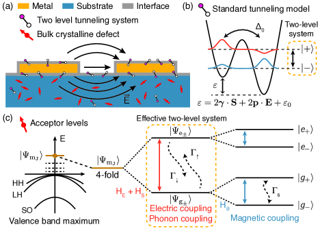
For superconducting microwave circuits operating at low temperature and in the single-photon regime, defect-induced dielectric loss can arise from coupling to TLSs and bulk crystalline defects (Fig. 1(a)). TLSs can be described by the standard tunneling model (STM) (Fig. 1(b)). They strongly couple to electric (E) and strain (S) fields through the asymmetry energy of the double-well potential: . Typical TLS has a deformation potential () of 1 eV [27] and an electric dipole moment (p) of 3 D [28]. The TLS can be described by the following Hamiltonian [29]:
| (1) |
where is the tunneling rate between the two potential wells, is the static asymmetry energy, is the energy splitting between the two levels, and denotes the Pauli operator. Due to their amorphous nature, TLS parameters are sampled from a broad distribution.
In contrast to highly disordered TLS defects in amorphous materials, silicon hosts high-quality spin (spin-orbit) qubits based on crystalline donor (acceptor) defects [30, 31, 32]. The electronic structure of donors and acceptors are well studied and can be used to predict their impact on superconducting circuits. Donor (e.g., phosphorus, bismuth) defects weakly couple to their environment via magnetic dipole interactions and show long spin lifetimes [30, 31, 33]. Magnetic dipole interactions are much weaker compared to electric dipole interactions, and the donor spin resonances are typically detuned from circuits at zero magnetic field. Donor defects therefore cannot result in the frequently observed saturable TLS loss in superconducting circuits. In contrast, other bulk crystalline defects can display Hamiltonians similar to TLSs and cause dielectric loss. In particular, acceptor (e.g., boron, aluminum) defects have strong electric and elastic dipoles, and therefore exhibit short lifetimes [34, 35, 36]. In this work, we investigate acceptors as a potential origin of a bulk TLS bath in silicon. Our study focuses on boron defects, one of the most common acceptor-type contaminants in silicon.
The electronic structure of boron acceptors inherits the properties of the valence band maximum of silicon (Fig. 1(c)). The ground state is an effective spin-3/2 system with a two-fold orbital degeneracy and a two-fold spin degeneracy. The linear coupling of the ground state to magnetic (), electric () and strain () fields can be described as [37]:
| (2) | ||||
| (3) | ||||
| (4) |
where is the spin-3/2 operator, denotes the anticommutator, c.p. denotes cyclic permutation, and are the g-factors [35], 0.26 D is the electric dipole moment [35], and eV and eV are deformation potentials [36]. The two-fold orbital degeneracy can be lifted with static lattice strain and/or electric field (), which results in a TLS-like level structure. Within each orbital branch, the spin degeneracy can be lifted with a static magnetic field (). The magnitudes of the electric dipole () and deformation potentials () for boron acceptors are similar to those of conventional TLSs (p and in Eq. 1) in amorphous materials. The strong correspondence in orbital structures and dipole strengths between borons and TLSs suggests that boron acceptors should lead to saturable dielectric loss like conventional TLSs.
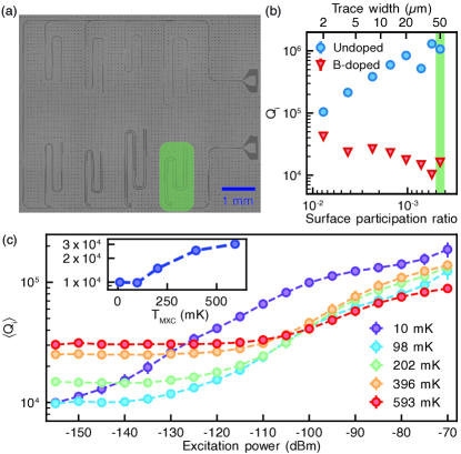
In the following, we test the hypothesis of boron acceptors constituting a bulk TLS bath and a strong dielectric loss channel. We use superconducting resonators to probe acceptor-induced loss under varying acceptor concentration, temperature, power, and magnetic fields. To access a bulk dielectric loss dominated regime, we first study the geometric dependence of loss under our fabrication procedure with quarter-wave resonators of varying dimensions (Fig. 2(a)) and frequencies ranging from 4.3 GHz to 7.7 GHz. For resonators on both undoped () and boron-doped () FZ silicon, we observe improvement of internal quality factors () at high excitation powers (see Supplemental Material Fig. S2 [38]). The power dependence shows the presence of TLS loss in both substrates. For undoped silicon, the single-photon scales inversely with the surface participation ratio, indicating the loss is dominated by surface TLSs (Fig. 2(b)) [10]. On boron-doped silicon, the single-photon does not show such an inverse scaling with surface participation (Fig. 2(b)). The energy participation in the bulk silicon substrate is independent of geometry and is near unity. The absence of negative correlation between the surface participation ratio and confirms that TLS loss is no longer surface limited on boron-doped silicon, and that we are probing TLSs in the bulk silicon substrate [17].
We use the resonator design with the lowest surface participation to probe bulk TLS loss in boron-doped silicon (). The sample contains eight quarter-wave resonators evenly spaced in a 1 GHz band centered around 6 GHz (see Supplemental Material Fig. S1(b) [38]). The average power-dependent of the resonators at different mixing chamber temperatures () is plotted in Fig. 2(c). For all resonators, consistently shows strong reduction at low powers. At the same time, low-power increases when thermal energy is comparable to the resonator frequency (Fig. 2(c), inset). This thermal saturation feature is another indication that bulk loss tangent in boron doped silicon is dominated by TLS-like atomic defects [5]. These observations confirm the TLS-acceptor correspondence discussed in Fig. 1, and we conclude that boron acceptors act as a TLS loss channel in the bulk substrate. We note that the bulk TLS loss from boron defects appears broadband ( GHz) based on the consistent saturation behaviors of resonators at different frequencies. This broadband behavior is likely related to a broad inhomogeneous distribution of boron orbital splittings due to an inhomogeneous strain distribution near the metal-silicon interface (see Supplemental Material Fig. S7 and Fig. S8 [39, 38]) and the local disorder in the environment of individual defects. Therefore, performing direct loss tangent measurement on low or high strain samples may reveal a different loss behavior [40, 16].
We quantify the impact of acceptor-induced dielectric loss on superconducting qubits by studying superconducting resonator low-power as a function of dopant type and doping concentration. Our first principles estimation (see Supplemental Material Sec. III C [38]) suggests acceptor-induced dielectric loss can be significant due to the near-unity energy participation of the bulk. However, the exact magnitude of acceptor-induced loss tangent strongly depends on the strain distribution and the electric dipole moment, and necessitates experimental characterization.
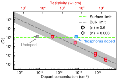
We fabricate resonators identical to the ones studied in Fig. 2(c) on undoped, phosphorus-doped, and boron-doped substrates [38]. The average low-power at mK as a function of doping concentration is summarized in Fig. 3. For undoped silicon and lightly boron-doped () silicon, low-power saturates around , consistent with the surface TLS limit in Fig. 2(b). For substrates with higher boron concentration, shows strong anti-correlation with boron concentration. This anti-correlation is consistent with the assignment of boron acceptors as a bulk TLS bath. We extrapolate the bulk limit of from boron doping for state-of-the-art devices using a linear fit of loss and boron doping. The extrapolation suggests bulk-limited would be limited to and for boron concentrations of and , respectively. We note that state-of-the-art quantum devices have lifetimes () around 1 ms, corresponding to a quality factor of at GHz. Based on our extrapolation and considering bulk dielectric loss alone, realizing such high-performance devices on silicon requires the use of ultra high-purity silicon with boron concentration below cm-3 (resistivity ). Further lifetime improvement will necessitate high-purity substrates free of boron defects and may require advancements in silicon wafer growth. We note that low-power of resonators on phosphorus doped silicon does not show excess loss from the bulk. The lack of phosphorus induced loss is consistent with the prediction based on its electronic structure which does not contain any orbital degeneracy in its ground state (see Supplemental Material Fig. S6 [41, 38]).
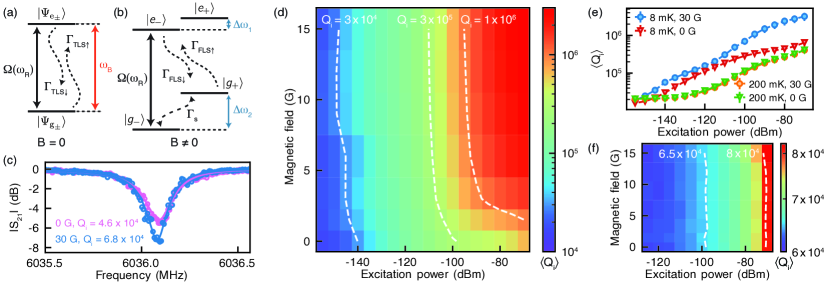
Having shown the bulk TLS behavior of boron acceptors, we turn to probing key distinctions between boron and conventional TLS [11]. In the following, we demonstrate that the spin-orbit coupling and four-level nature of boron acceptors leads to a strong magnetic field dependence of boron-induced dielectric loss. Fig. 4(a) shows the level structure of boron acceptors. Under zero magnetic field, the level structure resembles the structure of a conventional TLS, with stray strain and electric field determining the orbital splitting (). Magnetic fields lift spin degeneracies and result in a four-level structure (Fig. 4(b)). The effective g-factors within the two orbital branches are determined by the exact strain environment, which in general leads to unequal Zeeman splittings (). When the orbital splitting is much greater than spin splitting, the lower orbital branch exhibits two long-lived generalized spin states [32].
We fabricate resonators with narrow traces (10 m) and wide gaps (40 m) on boron-doped silicon () to study how the loss is modified under an in-plane magnetic field due to the four-level structure of boron. The narrow-trace geometry is chosen to mitigate vortex formation [42], while the wide-gap configuration helps maintain a low surface-participation ratio for detecting bulk loss. Under a small magnetic field (30 G), we observe an improvement in the low-power compared to the zero-field case (Fig. 4(c)). We further investigate how loss evolves under a magnetic field by measuring the power-dependent as a function of magnetic field (Fig. 4(d)). We observe three key features: (1) the saturation power of boron-induced loss is reduced by an order of magnitude under a non-zero magnetic field (Fig. 4(e) and Supplemental Material Fig. S10 [38]), (2) the loss reduction induced by magnetic field saturates at a magnetic field as low as 5 G, (3) high-power shows a drastic improvement under a magnetic field.
A simplified description of the change in saturation power in a magnetic field can be explained using the four-level system dynamics of boron acceptors in a magnetic field. Under zero magnetic field, boron acceptors are equivalent to standard TLSs. Driving the resonator at excites the nearby boron defects () with a rate . Acceptor-induced dielectric loss is saturated when the excitation rate is comparable to the fast orbital relaxation rate . For magnetic fields where the differential Zeeman splitting becomes greater than the resonator and boron linewidths ( G), transition associated with one of the ground states () is selectively driven. Therefore, the ground state population is pumped to the other long-lived dark state () with a rate of . Such microwave pumped boron acceptors are trapped in and decoupled from the resonator. This decrease of the effective number of TLSs results in reduced dielectric loss. In addition, the loss saturation occurs at a lower power where the pumping rate equals the dark state decay rate (), assuming . We use the measured ratio of saturation powers with and without magnetic fields to estimate the thermal occupancy () and the effective sample temperature. Our master equation model for four-level system saturation indicates an effective sample temperature of mK based on the measured saturation power ratios (see Supplemental Material Fig. S10 for a detailed analysis [38]). At elevated temperatures, the magnetic response becomes weaker (see Supplemental Material Fig. S5 [38]) due to exponential activation of thermal occupancy and where . We observe a complete disappearance of dielectric loss reduction in response to magnetic field at mK (Fig. 4(e)). Finally, we note that the loss reduction is higher at higher excitation powers, which may be accounted by the reduction of loss from a large ensemble of off-resonant boron acceptors.
We also perform a magnetic field study of conventional TLSs at surfaces. To our knowledge, magnetic response of such amorphous TLSs has not been reported before. We intentionally introduce a high density of amorphous TLSs by drop casting Hydrogen Silsesquioxane (HSQ) on high-Q resonators fabricated on undoped silicon (see Supplemental Material Fig. S1(d) [38]). In contrast to the acceptor-induced loss, the HSQ-induced loss remains constant in small magnetic fields (Fig. 4(f)). We emphasize that the lack of magnetic field response in our experimental regime cannot rule out the existence of magnetic dipole moments in amorphous TLSs. Instead, the observation indicates that surface TLSs do not have a differential Zeeman splitting in different orbital states (Fig. 4(b)).
In conclusion, we report the first microscopic identification of a TLS bath from bulk crystalline defects in silicon. Our study indicates that the acceptor-induced loss can act as a near-future limiting factor for state-of-the-art superconducting quantum devices on silicon. We show that the acceptor-induced dielectric loss can be reduced under a small magnetic field. These results also show the need for ultrahigh purity silicon wafers to enable next-generation superconducting qubits. We note that our observations apply to other acceptors in silicon which display similar electronic structures [43, 44]. In addition to improvements to substrate purity, further loss suppression can be achieved using vacuum-gap capacitors [45] or engineering the acceptor dynamics with phononic crystals [46, 47]. Finally, further engineering of interactions with boron acceptors can enable their use as spin-orbit qubits strongly coupled to microwave and mechanical resonators [48, 49, 50, 51, 32, 52, 53].
Acknowledgements.
We thank Xueyue Zhang for fruitful discussions, as well as Mi Lei and Shimon Kolkowitz for feedback on the manuscript. This work was primarily funded by the U.S. Department of Energy, Office of Science, Basic Energy Sciences, Materials Sciences and Engineering Division under Contract No. DE-AC02-05CH11231 within the Nanomachine Program (device design and measurements). Material characterization (SRIM) and cryogenic RF instrumentation is supported by the U.S. Department of Energy, Office of Science, Office of Basic Energy Sciences, Materials Sciences and Engineering Division under Contract No. DE-AC02-05-CH11231 in the Phonon Control for Next-Generation Superconducting Systems and Sensors FWP (KCAS23). Additional support was provided for device fabrication by the ONR and AFOSR Quantum Phononics MURI program for lithography development. The devices used in this work were fabricated at UC Berkeley’s NanoLab.References
- Arute et al. [2019] F. Arute, K. Arya, R. Babbush, D. Bacon, J. C. Bardin, R. Barends, R. Biswas, S. Boixo, F. G. S. L. Brandao, D. A. Buell, et al., Quantum supremacy using a programmable superconducting processor, Nature 574, 505 (2019).
- Kim et al. [2023] Y. Kim, A. Eddins, S. Anand, K. X. Wei, E. Van Den Berg, S. Rosenblatt, H. Nayfeh, Y. Wu, M. Zaletel, K. Temme, and A. Kandala, Evidence for the utility of quantum computing before fault tolerance, Nature 618, 500 (2023).
- Arute et al. [2020] F. Arute, K. Arya, R. Babbush, D. Bacon, J. C. Bardin, R. Barends, S. Boixo, M. Broughton, B. B. Buckley, D. A. Buell, et al., Hartree-fock on a superconducting qubit quantum computer, Science 369, 1084 (2020).
- Acharya et al. [2023] R. Acharya, I. Aleiner, R. Allen, T. I. Andersen, M. Ansmann, F. Arute, K. Arya, A. Asfaw, J. Atalaya, R. Babbush, et al., Suppressing quantum errors by scaling a surface code logical qubit, Nature 614, 676 (2023).
- McRae et al. [2020] C. R. H. McRae, H. Wang, J. Gao, M. R. Vissers, T. Brecht, A. Dunsworth, D. P. Pappas, and J. Mutus, Materials loss measurements using superconducting microwave resonators, Review of Scientific Instruments 91, 091101 (2020).
- Siddiqi [2021] I. Siddiqi, Engineering high-coherence superconducting qubits, Nature Reviews Materials 6, 875 (2021).
- Phillips [1972] W. A. Phillips, Tunneling states in amorphous solids, Journal of Low Temperature Physics 7, 351 (1972).
- Anderson et al. [1972] P. W. Anderson, B. I. Halperin, and C. M. Varma, Anomalous low-temperature thermal properties of glasses and spin glasses, The Philosophical Magazine: A Journal of Theoretical Experimental and Applied Physics 25, 1 (1972).
- Gao et al. [2008] J. Gao, M. Daal, A. Vayonakis, S. Kumar, J. Zmuidzinas, B. Sadoulet, B. A. Mazin, P. K. Day, and H. G. Leduc, Experimental evidence for a surface distribution of two-level systems in superconducting lithographed microwave resonators, Applied Physics Letters 92, 152505 (2008).
- Wang et al. [2015] C. Wang, C. Axline, Y. Y. Gao, T. Brecht, Y. Chu, L. Frunzio, M. H. Devoret, and R. J. Schoelkopf, Surface participation and dielectric loss in superconducting qubits, Applied Physics Letters 107, 162601 (2015).
- Müller et al. [2019] C. Müller, J. H. Cole, and J. Lisenfeld, Towards understanding two-level-systems in amorphous solids: insights from quantum circuits, Reports on Progress in Physics 82, 124501 (2019).
- Martinis et al. [2005] J. M. Martinis, K. B. Cooper, R. McDermott, M. Steffen, M. Ansmann, K. D. Osborn, K. Cicak, S. Oh, D. P. Pappas, R. W. Simmonds, and C. C. Yu, Decoherence in Josephson Qubits from Dielectric Loss, Physical Review Letters 95, 210503 (2005).
- Place et al. [2021] A. P. M. Place, L. V. H. Rodgers, P. Mundada, B. M. Smitham, M. Fitzpatrick, Z. Leng, A. Premkumar, J. Bryon, A. Vrajitoarea, S. Sussman, G. Cheng, T. Madhavan, H. K. Babla, X. H. Le, Y. Gang, B. Jäck, A. Gyenis, N. Yao, R. J. Cava, N. P. De Leon, and A. A. Houck, New material platform for superconducting transmon qubits with coherence times exceeding 0.3 milliseconds, Nature Communications 12, 1779 (2021).
- Martinis [2022] J. M. Martinis, Surface loss calculations and design of a superconducting transmon qubit with tapered wiring, npj Quantum Information 8, 26 (2022).
- Ganjam et al. [2023] S. Ganjam, Y. Wang, Y. Lu, A. Banerjee, C. U. Lei, L. Krayzman, K. Kisslinger, C. Zhou, R. Li, Y. Jia, M. Liu, L. Frunzio, and R. J. Schoelkopf, Surpassing millisecond coherence times in on-chip superconducting quantum memories by optimizing materials, processes, and circuit design (2023), arXiv:2308.15539.
- Read et al. [2023] A. P. Read, B. J. Chapman, C. U. Lei, J. C. Curtis, S. Ganjam, L. Krayzman, L. Frunzio, and R. J. Schoelkopf, Precision Measurement of the Microwave Dielectric Loss of Sapphire in the Quantum Regime with Parts-per-Billion Sensitivity, Physical Review Applied 19, 034064 (2023).
- Crowley et al. [2023] K. D. Crowley, R. A. McLellan, A. Dutta, N. Shumiya, A. P. M. Place, X. H. Le, Y. Gang, T. Madhavan, M. P. Bland, R. Chang, N. Khedkar, Y. C. Feng, E. A. Umbarkar, X. Gui, L. V. H. Rodgers, Y. Jia, M. M. Feldman, S. A. Lyon, M. Liu, R. J. Cava, A. A. Houck, and N. P. De Leon, Disentangling Losses in Tantalum Superconducting Circuits, Physical Review X 13, 041005 (2023).
- Bergeron et al. [2020] L. Bergeron, C. Chartrand, A. T. K. Kurkjian, K. J. Morse, H. Riemann, N. V. Abrosimov, P. Becker, H.-J. Pohl, M. L. W. Thewalt, and S. Simmons, Silicon-Integrated Telecommunications Photon-Spin Interface, PRX Quantum 1, 020301 (2020).
- Redjem et al. [2020] W. Redjem, A. Durand, T. Herzig, A. Benali, S. Pezzagna, J. Meijer, A. Yu. Kuznetsov, H. S. Nguyen, S. Cueff, J.-M. Gérard, I. Robert-Philip, B. Gil, D. Caliste, P. Pochet, M. Abbarchi, V. Jacques, A. Dréau, and G. Cassabois, Single artificial atoms in silicon emitting at telecom wavelengths, Nature Electronics 3, 738 (2020).
- Komza et al. [2022] L. Komza, P. Samutpraphoot, M. Odeh, Y.-L. Tang, M. Mathew, J. Chang, H. Song, M.-K. Kim, Y. Xiong, G. Hautier, and A. Sipahigil, Indistinguishable photons from an artificial atom in silicon photonics (2022), arxiv:2211.09305 .
- Higginbottom et al. [2022] D. B. Higginbottom, A. T. K. Kurkjian, C. Chartrand, M. Kazemi, N. A. Brunelle, E. R. MacQuarrie, J. R. Klein, N. R. Lee-Hone, J. Stacho, M. Ruether, C. Bowness, L. Bergeron, A. DeAbreu, S. R. Harrigan, J. Kanaganayagam, D. W. Marsden, T. S. Richards, L. A. Stott, S. Roorda, K. J. Morse, M. L. W. Thewalt, and S. Simmons, Optical observation of single spins in silicon, Nature 607, 266 (2022).
- Mi et al. [2018] X. Mi, M. Benito, S. Putz, D. M. Zajac, J. M. Taylor, G. Burkard, and J. R. Petta, A coherent spin–photon interface in silicon, Nature 555, 599 (2018).
- Eichenfield et al. [2009] M. Eichenfield, J. Chan, R. M. Camacho, K. J. Vahala, and O. Painter, Optomechanical crystals, Nature 462, 78 (2009).
- Gambetta et al. [2017] J. M. Gambetta, C. E. Murray, Y.-K.-K. Fung, D. T. McClure, O. Dial, W. Shanks, J. W. Sleight, and M. Steffen, Investigating Surface Loss Effects in Superconducting Transmon Qubits, IEEE Transactions on Applied Superconductivity 27, 1 (2017).
- Woods et al. [2019] W. Woods, G. Calusine, A. Melville, A. Sevi, E. Golden, D. Kim, D. Rosenberg, J. Yoder, and W. Oliver, Determining Interface Dielectric Losses in Superconducting Coplanar-Waveguide Resonators, Physical Review Applied 12, 014012 (2019).
- Melville et al. [2020] A. Melville, G. Calusine, W. Woods, K. Serniak, E. Golden, B. M. Niedzielski, D. K. Kim, A. Sevi, J. L. Yoder, E. A. Dauler, and W. D. Oliver, Comparison of dielectric loss in titanium nitride and aluminum superconducting resonators, Applied Physics Letters 117, 124004 (2020).
- Jäckle [1972] J. Jäckle, On the ultrasonic attenuation in glasses at low temperatures, Zeitschrift für Physik A Hadrons and nuclei 257, 212 (1972).
- Sarabi et al. [2016] B. Sarabi, A. N. Ramanayaka, A. L. Burin, F. C. Wellstood, and K. D. Osborn, Projected Dipole Moments of Individual Two-Level Defects Extracted Using Circuit Quantum Electrodynamics, Physical Review Letters 116, 167002 (2016).
- Phillips [1987] W. A. Phillips, Two-level states in glasses, Reports on Progress in Physics 50, 1657 (1987).
- Muhonen et al. [2014] J. T. Muhonen, J. P. Dehollain, A. Laucht, F. E. Hudson, R. Kalra, T. Sekiguchi, K. M. Itoh, D. N. Jamieson, J. C. McCallum, A. S. Dzurak, and A. Morello, Storing quantum information for 30 seconds in a nanoelectronic device, Nature Nanotechnology 9, 986 (2014).
- Wolfowicz et al. [2013] G. Wolfowicz, A. M. Tyryshkin, R. E. George, H. Riemann, N. V. Abrosimov, P. Becker, H.-J. Pohl, M. L. W. Thewalt, S. A. Lyon, and J. J. L. Morton, Atomic clock transitions in silicon-based spin qubits, Nature Nanotechnology 8, 561 (2013).
- Kobayashi et al. [2021] T. Kobayashi, J. Salfi, C. Chua, J. Van Der Heijden, M. G. House, D. Culcer, W. D. Hutchison, B. C. Johnson, J. C. McCallum, H. Riemann, N. V. Abrosimov, P. Becker, H.-J. Pohl, M. Y. Simmons, and S. Rogge, Engineering long spin coherence times of spin–orbit qubits in silicon, Nature Materials 20, 38 (2021).
- Mansir et al. [2018] J. Mansir, P. Conti, Z. Zeng, J. J. Pla, P. Bertet, M. W. Swift, C. G. Van De Walle, M. L. W. Thewalt, B. Sklenard, Y. M. Niquet, and J. J. L. Morton, Linear Hyperfine Tuning of Donor Spins in Silicon Using Hydrostatic Strain, Physical Review Letters 120, 167701 (2018).
- Song and Golding [2011] Y. P. Song and B. Golding, Manipulation and decoherence of acceptor states in silicon, Europhysics Letters 95, 47004 (2011).
- Köpf and Lassmann [1992] A. Köpf and K. Lassmann, Linear Stark and nonlinear Zeeman coupling to the ground state of effective mass acceptors in silicon, Physical Review Letters 69, 1580 (1992).
- Neubrand [1978] H. Neubrand, ESR From boron in silicon at zero and small external stress I. Line positions and line structure, physica status solidi (b) 86, 269 (1978).
- Bir et al. [1974] G. L. Bir, G. E. Pikus, J. C. Hensel, P. Shelnitz, and D. Louvish, Symmetry and strain-induced effects in semiconductors (Wiley, New York, 1974).
- [38] See Supplemental Material for supplementary methods, measurements, and theoretical analyses.
- Pla et al. [2018] J. J. Pla, A. Bienfait, G. Pica, J. Mansir, F. A. Mohiyaddin, Z. Zeng, Y. M. Niquet, A. Morello, T. Schenkel, J. J. L. Morton, and P. Bertet, Strain-Induced Spin-Resonance Shifts in Silicon Devices, Physical Review Applied 9, 044014 (2018).
- Checchin et al. [2022] M. Checchin, D. Frolov, A. Lunin, A. Grassellino, and A. Romanenko, Measurement of the Low-Temperature Loss Tangent of High-Resistivity Silicon Using a High- Q Superconducting Resonator, Physical Review Applied 18, 034013 (2022).
- Aggarwal [1964] R. Aggarwal, Optical determination of the valley-orbit splitting of the ground state of donors in silicon, Solid State Communications 2, 163 (1964).
- Stan et al. [2004] G. Stan, S. B. Field, and J. M. Martinis, Critical Field for Complete Vortex Expulsion from Narrow Superconducting Strips, Physical Review Letters 92, 097003 (2004).
- Bir et al. [1963a] G. Bir, E. Butikov, and G. Pikus, Spin and combined resonance on acceptor centres in Ge and Si type crystals—I, Journal of Physics and Chemistry of Solids 24, 1467 (1963a).
- Bir et al. [1963b] G. Bir, E. Butikov, and G. Pikus, Spin and combined resonance on acceptor centres in Ge and Si type crystals—II, Journal of Physics and Chemistry of Solids 24, 1475 (1963b).
- Zemlicka et al. [2023] M. Zemlicka, E. Redchenko, M. Peruzzo, F. Hassani, A. Trioni, S. Barzanjeh, and J. Fink, Compact vacuum-gap transmon qubits: Selective and sensitive probes for superconductor surface losses, Physical Review Applied 20, 044054 (2023).
- Chen et al. [2023] M. Chen, J. C. Owens, H. Putterman, M. Schäfer, and O. Painter, Phonon engineering of atomic-scale defects in superconducting quantum circuits (2023), arxiv:2310.03929 .
- Odeh et al. [2023] M. Odeh, K. Godeneli, E. Li, R. Tangirala, H. Zhou, X. Zhang, Z.-H. Zhang, and A. Sipahigil, Non-Markovian dynamics of a superconducting qubit in a phononic bandgap (2023), arxiv:2312.01031 .
- Ruskov and Tahan [2013] R. Ruskov and C. Tahan, On-chip cavity quantum phonodynamics with an acceptor qubit in silicon, Physical Review B 88, 064308 (2013).
- Van Der Heijden et al. [2014] J. Van Der Heijden, J. Salfi, J. A. Mol, J. Verduijn, G. C. Tettamanzi, A. R. Hamilton, N. Collaert, and S. Rogge, Probing the Spin States of a Single Acceptor Atom, Nano Letters 14, 1492 (2014).
- Salfi et al. [2016a] J. Salfi, J. A. Mol, D. Culcer, and S. Rogge, Charge-Insensitive Single-Atom Spin-Orbit Qubit in Silicon, Physical Review Letters 116, 246801 (2016a).
- Salfi et al. [2016b] J. Salfi, M. Tong, S. Rogge, and D. Culcer, Quantum computing with acceptor spins in silicon, Nanotechnology 27, 244001 (2016b).
- Zhang et al. [2023] S. Zhang, Y. He, and P. Huang, Acceptor-based qubit in silicon with tunable strain, Physical Review B 107, 155301 (2023).
- Samkharadze et al. [2016] N. Samkharadze, A. Bruno, P. Scarlino, G. Zheng, D. P. DiVincenzo, L. DiCarlo, and L. M. K. Vandersypen, High-Kinetic-Inductance Superconducting Nanowire Resonators for Circuit QED in a Magnetic Field, Physical Review Applied 5, 044004 (2016).