Toward High Performance, Programmable Extreme-Edge Intelligence for Neuromorphic Vision Sensors utilizing Magnetic Domain Wall Motion-based MTJ
Abstract
The desire to empower resource-limited edge devices with computer vision (CV) must overcome the high energy consumption of collecting and processing vast sensory data. To address the challenge, this work proposes an energy-efficient non-von-Neumann in-pixel processing solution for neuromorphic vision sensors employing emerging (X) magnetic domain wall magnetic tunnel junction (MDWMTJ) for the first time, in conjunction with CMOS-based neuromorphic pixels. Our hybrid CMOS+X approach performs in-situ massively parallel asynchronous analog convolution, exhibiting low power consumption and high accuracy across various CV applications by leveraging the non-volatility and programmability of the MDWMTJ. Moreover, our developed device-circuit-algorithm co-design framework captures device constraints (low tunnel-magnetoresistance, low dynamic range) and circuit constraints (non-linearity, process variation, area consideration) based on monte-carlo simulations and device parameters utilizing GF22nm FD-SOI technology. Our experimental results suggest we can achieve an average of 45.3% reduction in backend-processor energy, maintaining similar front-end energy compared to the state-of-the-art and high accuracy of 79.17% and 95.99% on the DVS-CIFAR10 and IBM DVS128-Gesture datasets, respectively.
Keywords Neuromorphic, Convolution, In-pixel Processing, Magnetic Domain Wall MTJ, Device-Circuit-Algorithm Co-design.
1 Introduction
Edge devices with computer vision (CV) systems face energy inefficiency and throughput bottlenecks due to physically segregated sensor hardware and processing platforms Chai (2020). To address this, researchers have explored near-sensor, in-sensor, and in-pixel processing methods Eki et al. (2021); Lefebvre et al. (2021); Tabrizchi et al. (2023); Datta et al. (2022a); Hsu et al. (2022). While near-sensor and in-sensor approaches still encounter bandwidth challenges, in-pixel processing allows simultaneous sensing and computing within the pixel array, providing energy-efficient processing by transmitting feature outputs instead of raw sensory data. In the realm of CMOS Image Sensors (CIS), bio-inspired event-based neuromorphic vision sensors (NVS) Lichtsteiner et al. (2008); Leñero-Bardallo et al. (2011) have gained popularity over traditional CIS for various neural network (NN) applications Chen et al. (2020); Nguyen et al. (2019); Maqueda et al. (2018) due to their lower latency, energy efficiency, high temporal precision, and dynamic range. In summary, integrating neuromorphic vision sensors with in-pixel processing presents a comprehensive solution to energy inefficiency and throughput bottlenecks in resource-constrained edge devices with CV systems.
Neuromorphic vision sensors often utilize spiking convolutional neural networks (CNNs) for processing asynchronous input events. In the traditional approach, the duration of the neuromorphic datasets is segmented into predetermined integration intervals, accumulating input spikes within each period to generate multi-bit inputs for the initial layer of the spiking CNN Datta et al. (2022b). Unlike subsequent layers that consist of energy-efficient accumulators, the first layer involves digital multi-bit Multiply-Accumulate (MAC) operations. To enhance energy efficiency in the first layer, analog MAC units, employing continuous variables like current, resistance, or pulse width as weights and capacitors as accumulators (representing the membrane potential), can be utilized in CNN hardware implementations Lefebvre et al. (2021); Hsu et al. (2022); Song et al. (2022); Zhang et al. (2022); Hsu et al. (2020); Kaiser et al. (2023). Substantial energy consumption may result from the active amplifier-based capacitor; in contrast, the passive capacitor-based accumulator yields low-energy consumption. However, the passive capacitor cannot retain the charge (membrane potential) for a long duration due to the leakage of the CMOS circuits, resulting in lower overall classification accuracy.
Due to the limitations of the CMOS circuits including the inherent leakage, research is shifting towards NN architectures utilizing emerging (X) post-CMOS technologies such as Phase Change Memories (PCM), Resistive Random Access Memory (RRAM), Magnetic Tunnel Junction (MTJ), Magnetic Domain Wall (MDW), etc. Roy et al. (2020); Ankit et al. (2017); Sengupta et al. (2016); Leonard et al. (2022). The benefits of non-volatility, reduced power consumption, higher density, speed, and CMOS compatibility drive this shift. Spintronics devices offer lower latency, reduced energy dissipation, and unlimited endurance compared to other emerging technologies; however, they suffer from a low on-off ratio due to low TMR (between 200% and 600% Alamdar et al. (2021); Ikeda et al. (2008)). Spintronic device magnetic domain wall magnetic tunnel junction (MDWMTJ) demonstrates a continuous resistance state based on domain wall position and has experimentally demonstrated good accuracy in neuromorphic applications Leonard et al. (2022); Alamdar et al. (2021). In addition, hybrid CMOS and MDWMTJ structures are reported for logic, in-memory, and neuromorphic applications Sengupta et al. (2016); Hu et al. (2019); Wang et al. (2020). Considering these advantages, our proposed processing-in-pixel-in-memory (P2M) hardware for neuromorphic vision sensors utilizes MDWMTJ as the core component. Note, we choose spin-orbit-torque (SOT)-based MDWMTJ instead of spin-transfer-torque (STT)-based MDWMTJ due to their lower write current requirements and decoupled read and write path, resulting in low power dissipation and constant resistance along the write path that makes the associated CMOS circuit design easier.
This work presents an energy-efficient in-pixel processing hardware for spiking CNN focusing on neuromorphic vision applications. We utilize hybrid CMOS and MDWMTJ approaches to achieve high dynamic range, low energy consumption, and programmability for our neuromorphic CMOS+X P2M hardware. The key contributions of our work include the following:
-
1.
We propose a novel hybrid CMOS+X approach of processing-in-pixel-in-memory (P2M) for neuromorphic vision sensors, incorporating the emerging (X) magnetic domain wall magnetic tunnel junction (MDWMTJ) device as the core compute element for our developed spiking CNN framework. The non-volatility and programmability of the MDWMTJ enable the membrane potential to be retained for a longer integration time and tunable weight and neuron threshold, which are important for ensuring high accuracy.
-
2.
In addition, we design three current-based analog weight configurations: CMOS-based, MDWMTJ-based, and hybrid CMOS+X. Our hybrid symbiotic CMOS+X approach combines the unique benefits of both technologies, exhibiting close to state-of-the-art (SOTA) accuracy (thanks to the high dynamic range supported by the CMOS weights) while allowing mapping of multiple CV applications onto the same hardware (owing to the programmability of MDWMTJ).
-
3.
Finally, we develop a device-circuit-algorithm co-design solution incorporating the device constraints (low TMR, low dynamic range) and circuit constraints (non-linearity, process variations, area limitations based on the extensive monte-carlo simulations and parameters utilizing GF22nm FD-SOI technology node) into our algorithmic framework, resulting in an average of 45.3% reduction in backend-processor energy consumption on the NMNIST, CIFAR10-DVS, IBM DVS128-Gesture dataset, albeit with a 0.28%, 1.55%, and 1.23% in test accuracy drop from the baseline, respectively.
To the best of our knowledge, this is the first work to present a pathway towards attaining high-accuracy and programmability on complex neuromorphic datasets using in-pixel processing for NVS cameras leveraging a CMOS+X solution.
2 Device Preliminaries and Modeling
Figure 1(a) depicts the structure of a spin-orbit-torque (SOT)-based MDWMTJ. It consists of a thin insulating oxide layer between two ferromagnetic (FM) layers: a pinned layer (PL) with fixed magnetization and a free layer (FL) with parallel (P) and antiparallel (AP) magnetic domains. The AP domain has higher resistance due to the tunnel magnetoresistance (TMR) effect. A heavy metal (HM) layer below the FL influences the domain wall (DW) position through current-induced SOT and Dzyaloshinskii-Moriya interaction (DMI) Wang et al. (2020, 2021); Martinez et al. (2014). Unlike conventional MTJs, the MDW-MTJ exhibits continuous resistance states based on the DW position (q), allowing for multiple resistance levels, as experimentally demonstrated Leonard et al. (2022).
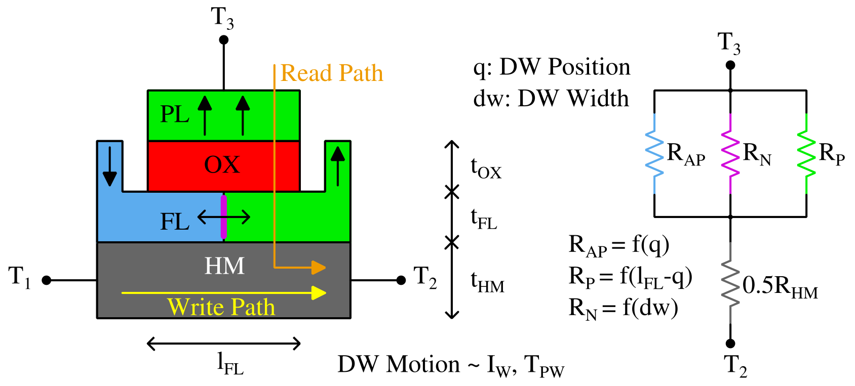
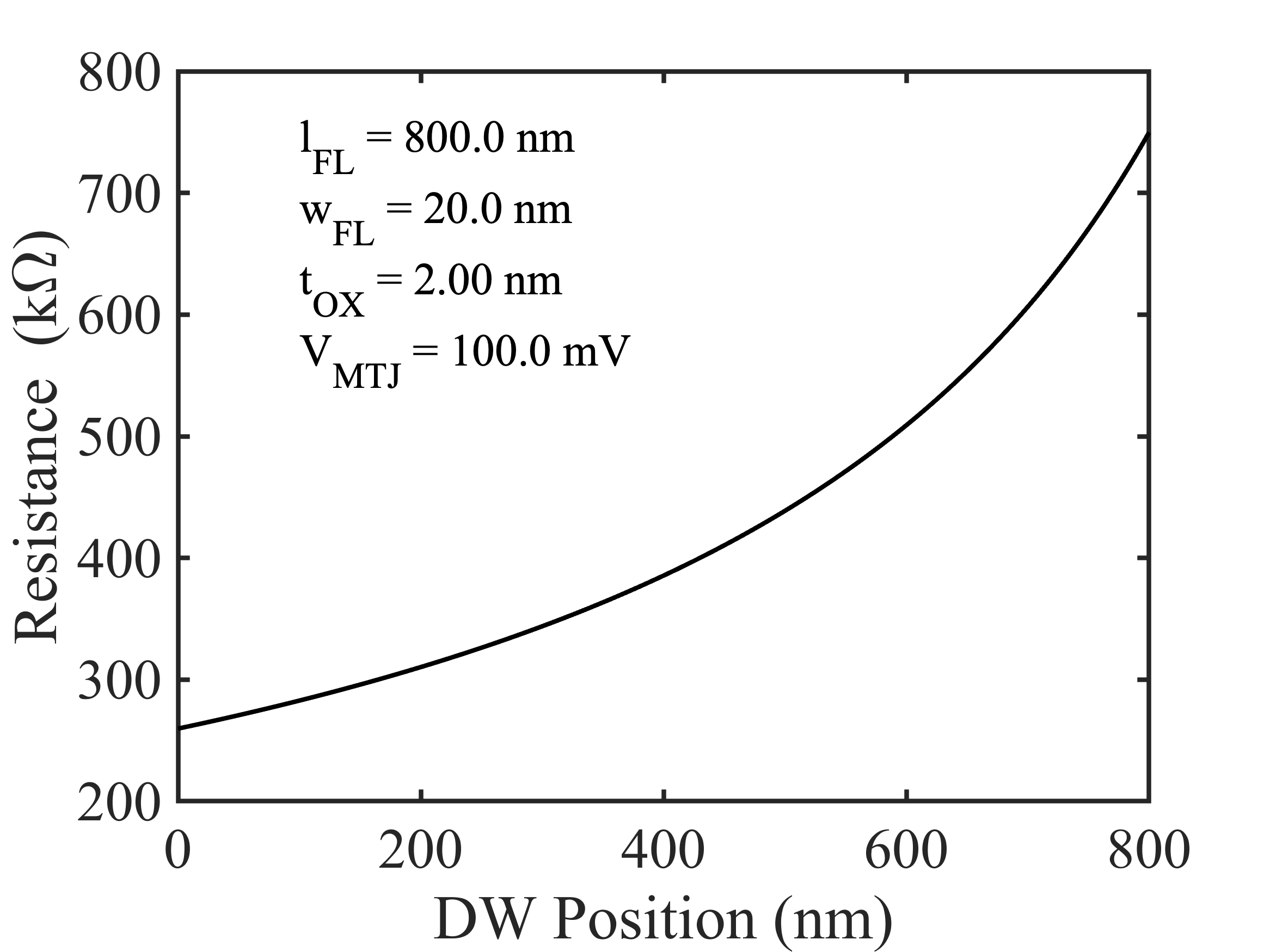
In the SOT-based MDWMTJ, the read and write paths are decoupled, allowing independent optimization. The DW position is programmed by applying a current pulse through the HM between the terminal T1 and T2 (Figure 1(a)), where the DW motion is proportional to pulse amplitude and duration. Our approach utilizes the T1 to T2 directed (positive direction) current flow for weighted accumulation, a configuration experimentally demonstrated in Luo et al. (2021). A long-duration current from T2 to T1 (negative direction) is applied to reset the DW position (q), which shifts the DW to the leftmost position (q = 0). The MDWMTJ resistance (between T3 and T2) is non-linearly dependent on DW position and applied voltage. At q = 0 and q = , MDWMTJ exhibits the lowest () and highest () resistance, respectively. For other DW positions (q), the resistance non-linearly varies between and .
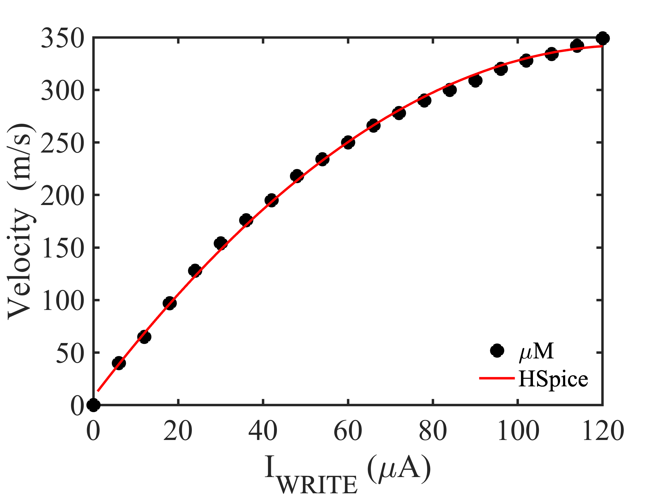
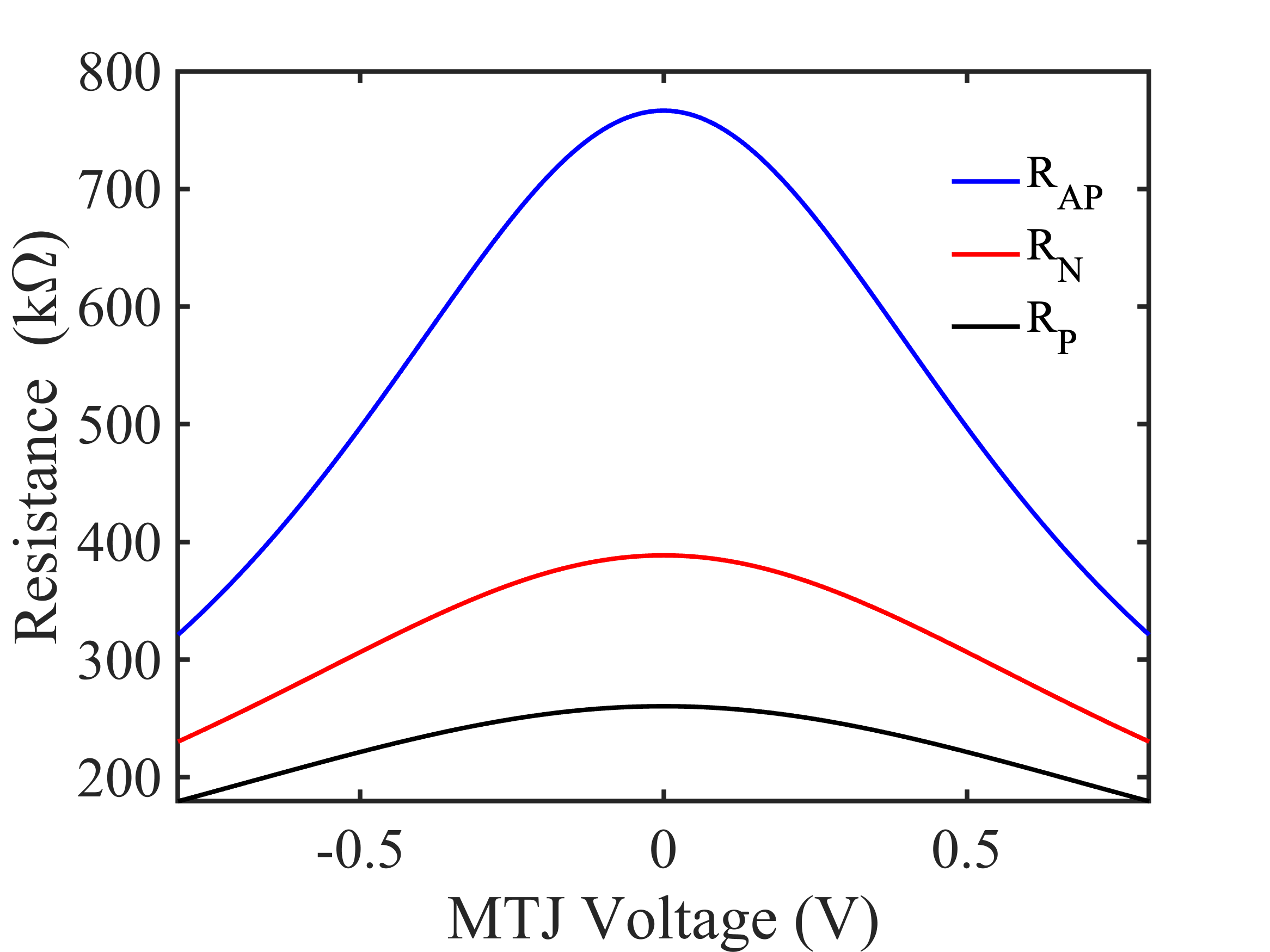
We developed a compact Verilog-A model of the MDWMTJ for HSpice simulations, benchmarking it with MuMax3 M results utilizing experimental device parameters from Wang et al. (2020). The Verilog-A model captures DW velocity as a function of the write current utilizing a 2nd-order polynomial fitting function (Figure 1(b)), demonstrating 1.06% of RMSE error. Using a resistance model that has been benchmarked to a non-equilibrium Green’s function (NEGF)-based framework from Fong et al. (2011), we simulated MTJ resistance across different applied voltages (Figure 1(c)). To determine the resistance of an MTJ in an FM with a domain wall between two oppositely polarized domains, the NEGF-based simulator is adapted to account for a parallel connection of three separate MTJs (parallel, anti-parallel, and perpendicular) Sengupta et al. (2016). The parallel and anti-parallel resistance varies as a function of the DW position, while the perpendicular resistance depends on the DW width. The effective MDWMTJ resistance, including the HM resistance as a function of the DW position, is shown in Figure 1(d). Our analysis utilizes the compact 3-terminal MDWMTJ Verilog-A model, capturing the DW dynamics and non-linear voltage-dependent resistance.
3 Proposed neuromorphic CMOS+X P2M Hardware Architecture
This section introduces the hardware innovations and implementation of our proposed CMOS+X spiking CNN architecture. The in-situ P2M hardware can be heterogeneously 3D integrated Miura et al. (2019); Kagawa et al. (2020) where the top die accommodates the NVS array, and the bottom die contains vertically aligned MAC units per the spiking CNN filter inputs (Figure 2). The sensor array generates an ON (OFF) event spike when the contrast detected by the neuromorphic pixel increases (decreases) by a certain threshold. The neuromorphic CMOS+X P2M core on the bottom die receives event spikes as inputs from the top die through hybrid Cu-Cu bonding. The P2M core consists of analog weights and accumulators to perform the MAC computations. The current represents the weight values encoded as device parameters, such as the width of CMOS transistors, or the resistance of the MDWMTJ, or both. The input-current-modulated DW motion of the MDWMTJ has been utilized as the accumulator.
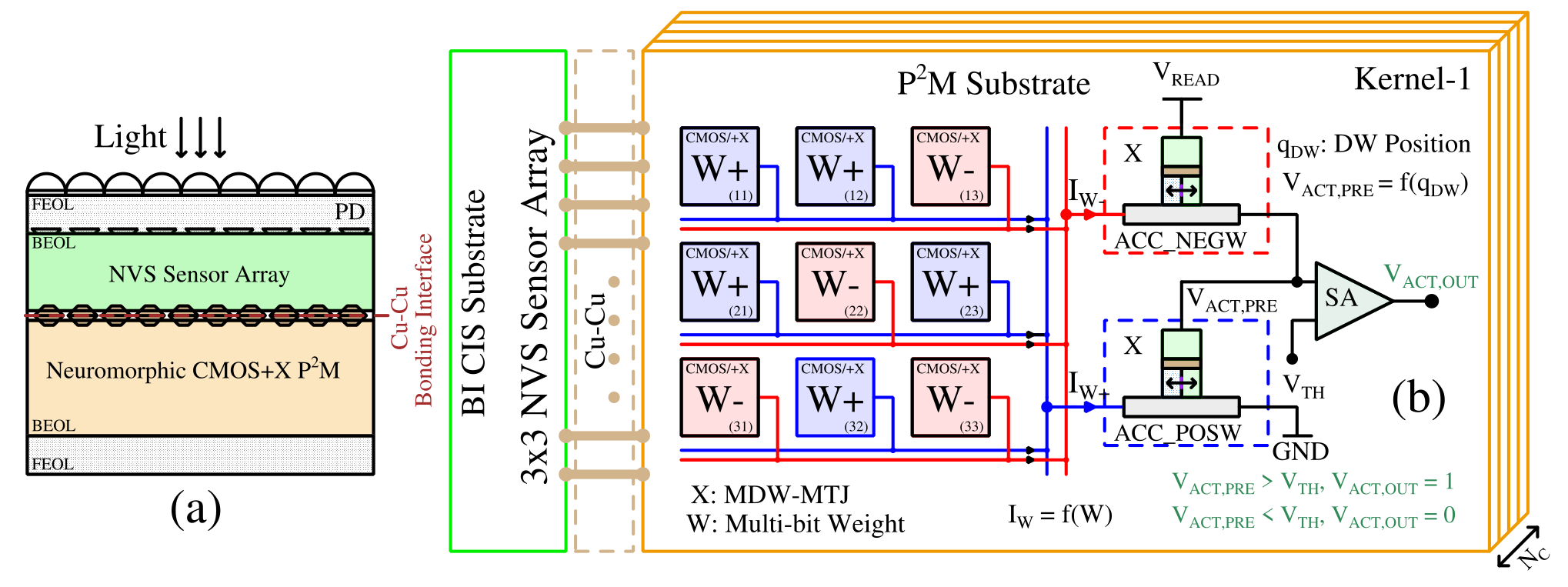
Spiking CNN requires asynchronous MAC computation and synchronous thresholding after a fixed integration time. Input event spikes trigger asynchronous write currents through the accumulator MDWMTJ, dependent on weight values. For large (small) weight values, large (small) write current () flows through the HM, resulting in large (small) DW motion from its previous state (position). As the input spikes are binary, DW motion represents the accumulated MAC output, with separate MDWMTJs for positive () and negative () weights. After the integration time, the pre-activation voltage (), non-linearly proportional to DW position differences of the positive and negative accumulators, is generated. Finally, a thresholding circuit compares the pre-activation voltage with the threshold, producing the output activation spike for the next layer if it exceeds the threshold. A tunable threshold per neuron is achieved using a series divider of two programmable MDWMTJs, which will be utilized in the algorithmic optimization, along with the programmable weights for catering to various applications.
The spiking CNN requires multiple channels in the first layer for improved accuracy. Each channel operates independently with its weights and accumulators, performing asynchronous MAC and synchronous thresholding in parallel. After the thresholding, one channel is activated at a time, and the output activations of the different channels are read sequentially utilizing the asynchronous Address-Event Representation (AER) read scheme Boahen (2004); Lichtsteiner et al. (2008) similar to the neuromorphic vision sensors. The output activation map is determined by kernel size and stride; hence, it is smaller than the raw sensor array. In addition, it eliminates the need for an extra bit to indicate event polarity (ON or OFF); hence, it reduces the number of required communicated off-chip address bits. Upon spike generation, a reset phase is executed for both positive and negative accumulators in the channel, involving a reset current flow in the negative direction to move the DW to the leftmost position.
3.1 In-situ Multi-bit Weights
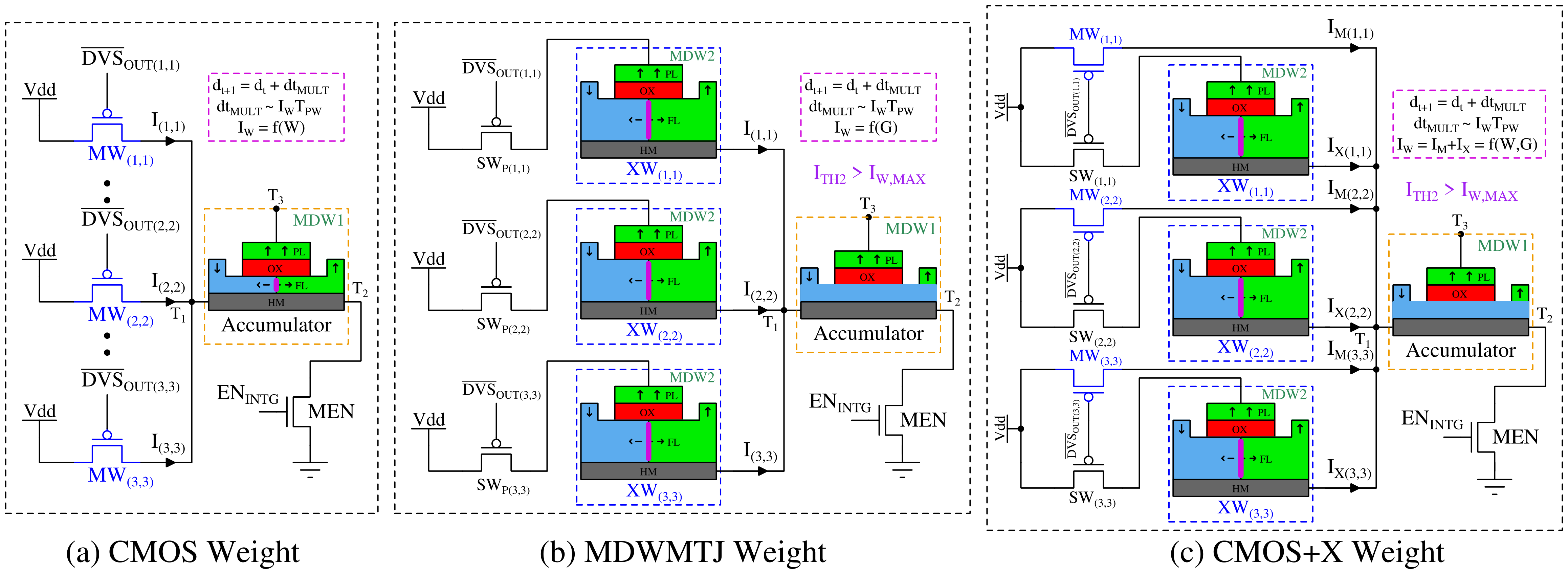
Figure 3 presents three configurations: CMOS, MDWMTJ, and Hybrid CMOS+X weights to perform the MAC operation. In the CMOS-based implementation, weights (e.g., , , ) are represented by the transistor’s width. The MDWMTJ-based configuration employs MDWMTJ as the weight (e.g., , , ), and the resistance state (DW position) of the MDWMTJ dictates the weight value. The threshold current of the weight MDWMTJs needs to be higher ( > ) to prevent the weight current from triggering the writing process into the weight MDWMTJ during MAC operations. The thickness of the FL can modulate the threshold current of the MDWMTJ Zhu et al. (2020). Though MDWMTJ-based configuration offers programmability, it exhibits a smaller dynamic range (due to low TMR Alamdar et al. (2021), TMR = 200% used in this work) than CMOS-based weights, which are fixed during the fabrication steps. To overcome these limitations and achieve versatility, we propose a hybrid CMOS+X configuration, combining transistor width and MDWMTJ resistance for adjustable write currents. This hybrid approach provides a broad dynamic range akin to CMOS-based weights and modest tunability (30-40% for most weight values) like the MDW-based weights, requiring device-algorithm co-design optimization for effective implementation across various applications. Positive (negative) weights are connected to the positive (negative) accumulator MDWMTJs. A larger weight value corresponds to a wider transistor or/and a lower MDWMTJ resistance, resulting in a higher current flowing through the HM of the accumulator MDWMTJs during an event spike. The DW motion, triggered by the input spike, moves from left to right and accumulates the MAC results throughout the integration time. Due to non-volatility, the accumulator MDWMTJs retain the previous membrane potential (DW position) for subsequent integration times, a behavior important for achieving a high classification accuracy.
3.2 Analog Convolution Operation
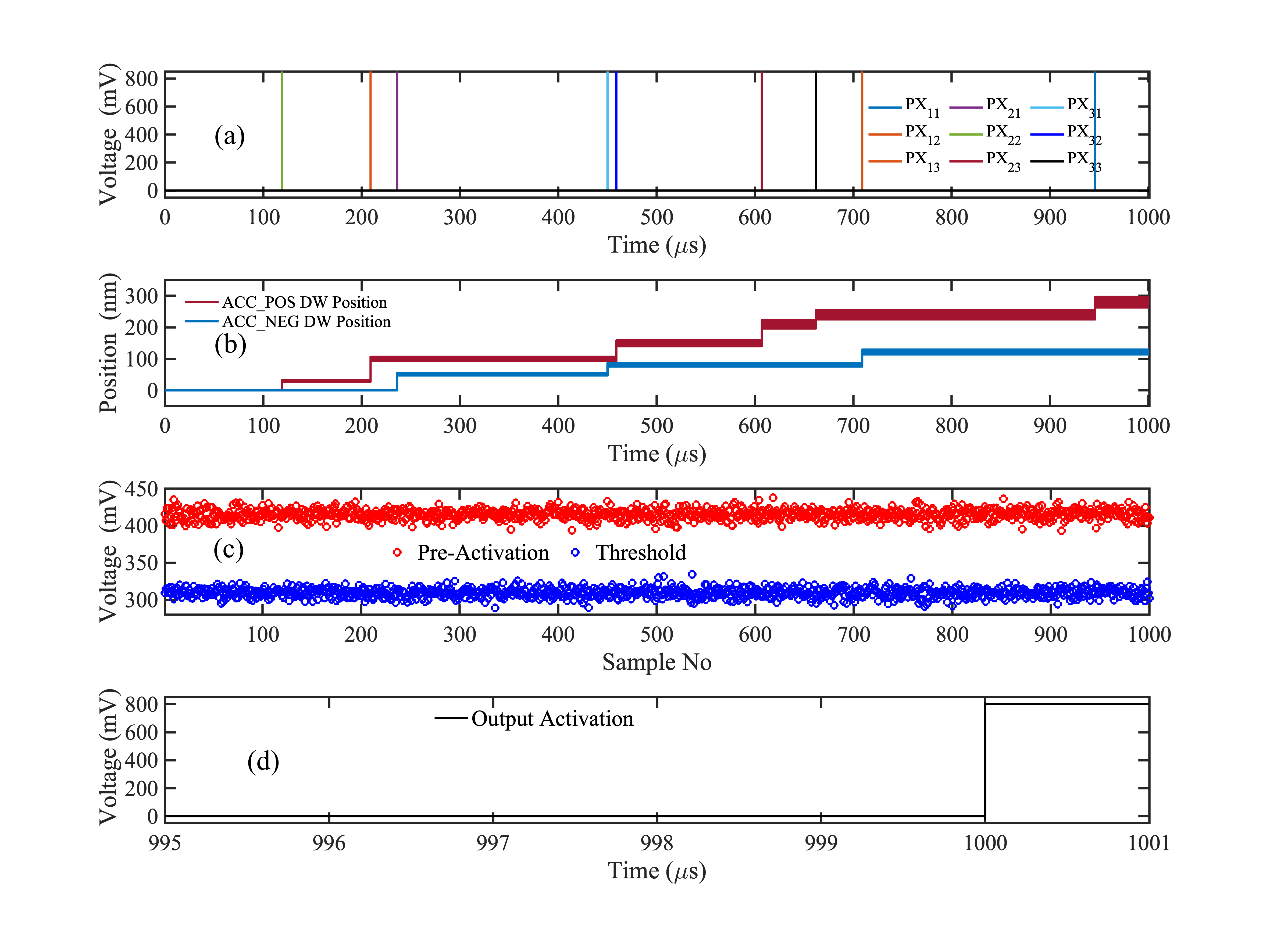
Figure 4 presents an HSpice simulation of our hybrid CMOS+X approach based on asynchronous MAC computations and synchronous output activation using GF22nm FD-SOI technology. The simulation considers a 33 kernel size, random positive and negative weights, and random event timings and includes transistor 3-sigma variation, 10% Gaussian jitter in the write pulse, and 20% resistance variations in MDWMTJs. Subplot (b) illustrates the rightward movement of positive and negative accumulators during event spikes, as seen in subplot (a). Despite using a 1 ms integration time for efficient 1000 monte-carlo simulations, the MDWMTJ’s non-volatility allows longer state retention, with cumulative CMOS leakage staying below the accumulator MDWMTJ’s threshold current, preventing any DW movement. After 1 ms of integration time, the reasonable sense margin between the final pre-activation and threshold voltage for 1000 samples (subplot (c)) leads to an output activation spike for the next layer (subplot (d)).
3.3 Reprogrammability of Weight and Neuron’s Threshold
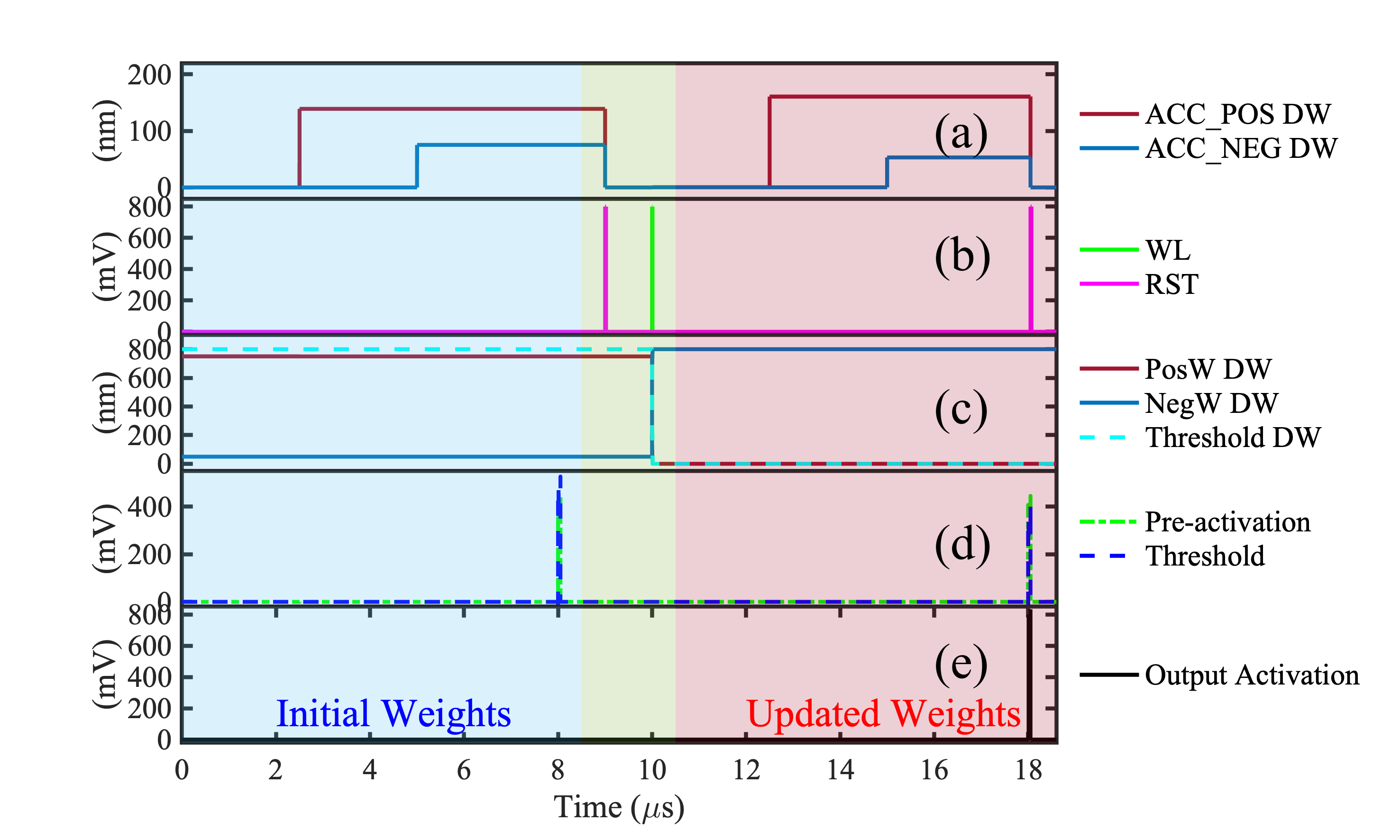
In Figure 5, we showcase the reprogrammability of weights and threshold voltage in our hybrid CMOS+X configuration, where we have utilized both CMOS and MDWMTJ as weights. The blue and red shaded regions represent MAC and thresholding operations for initial and updated setups, while the green region indicates the programmability of weights and threshold voltage, along with accumulator reset. One positive and one negative weight were randomly selected for this test. The transistor width is fixed in the CMOS+X hybrid configuration, and MDWMTJ resistance can be tuned for weight modulation. Initially (blue-shaded region), the MDWMTJ of the positive (negative) weight is set to a higher (lower) resistance state by programming the DW position. Depending on input event spikes, the DW of the positive (ACC_POS DW in subplot (a)) and negative (ACC_NEG DW in subplot (a)) accumulators moves rightward from their reset state. From subplots (d) and (e), it can be observed that the pre-activation voltage is smaller than the threshold voltage for the initial weight setup, resulting in an output activation of 0. The reset and programmable features are then demonstrated. The accumulators are reset, and the DW positions of the positive and negative MDWMTJ weights are programmed to different states within the tunable range (subplot (c)). Additionally, the DW position of the reference voltage generation is programmed to a lower resistance state to achieve a smaller neuron threshold. Due to the updated weights and threshold voltage, the MAC and threshold results differ from the previous application. The difference between the positive and negative accumulator has increased, leading to a higher pre-activation voltage, surpassing the lowered threshold voltage, and resulting in an output activation spike.
4 Device-Circuit-Algorithm Co-design
In this section, we detail the implementation of our algorithmic framework on the proposed neuromorphic CMOS+X P2M architecture, considering both device and circuit constraints. We address the non-ideal, non-linear attributes of MDWMTJ and transistors, incorporating process variations to account for potential resistance and current deviations in our CMOS+X system. Through extensive HSpice simulations on the GF22nm FD-SOI node, we map and integrate our circuit characteristics into our spiking CNN framework, utilizing custom functions that adapt to circuit and device non-linearity, non-ideality, and variations.
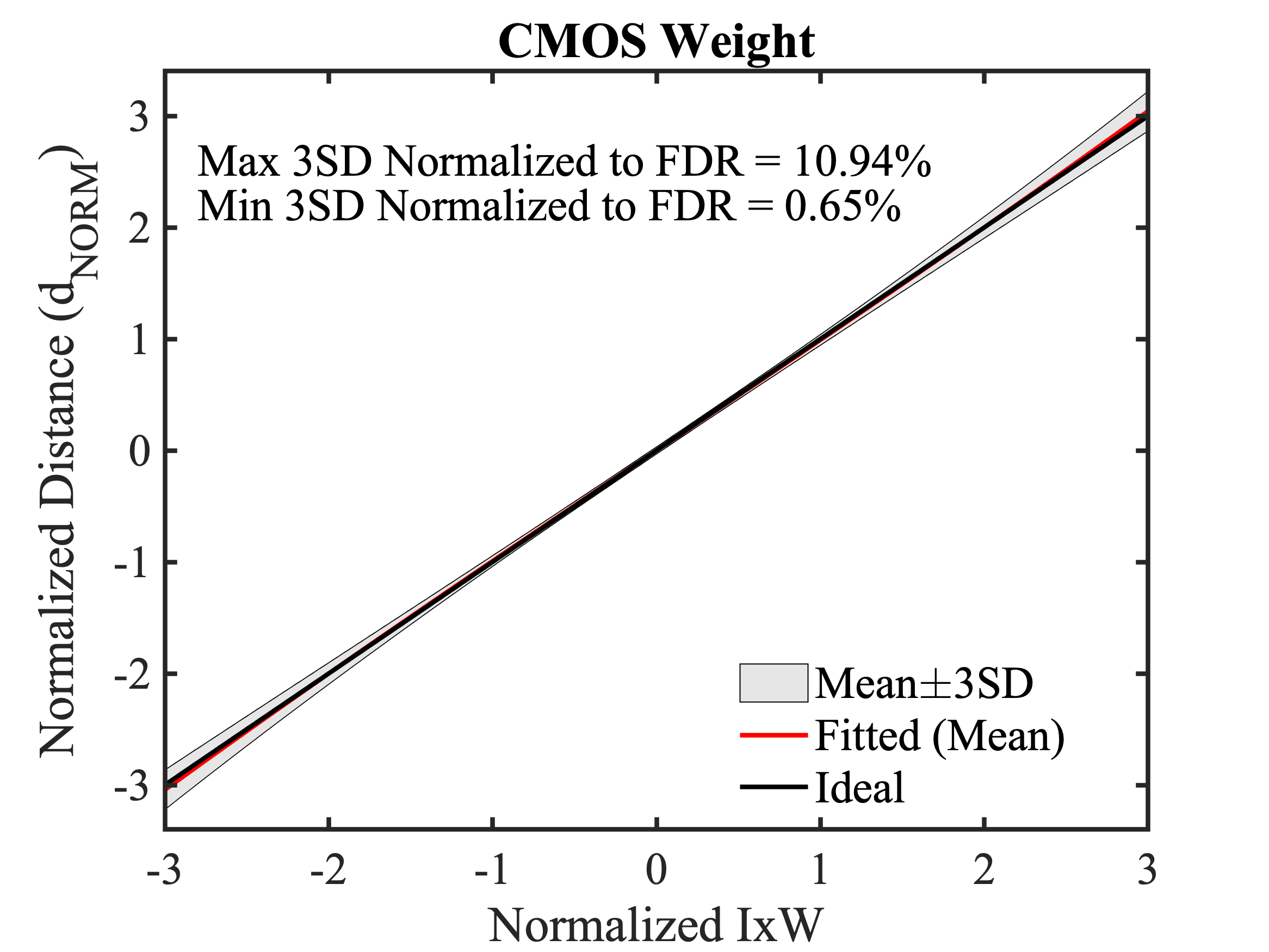
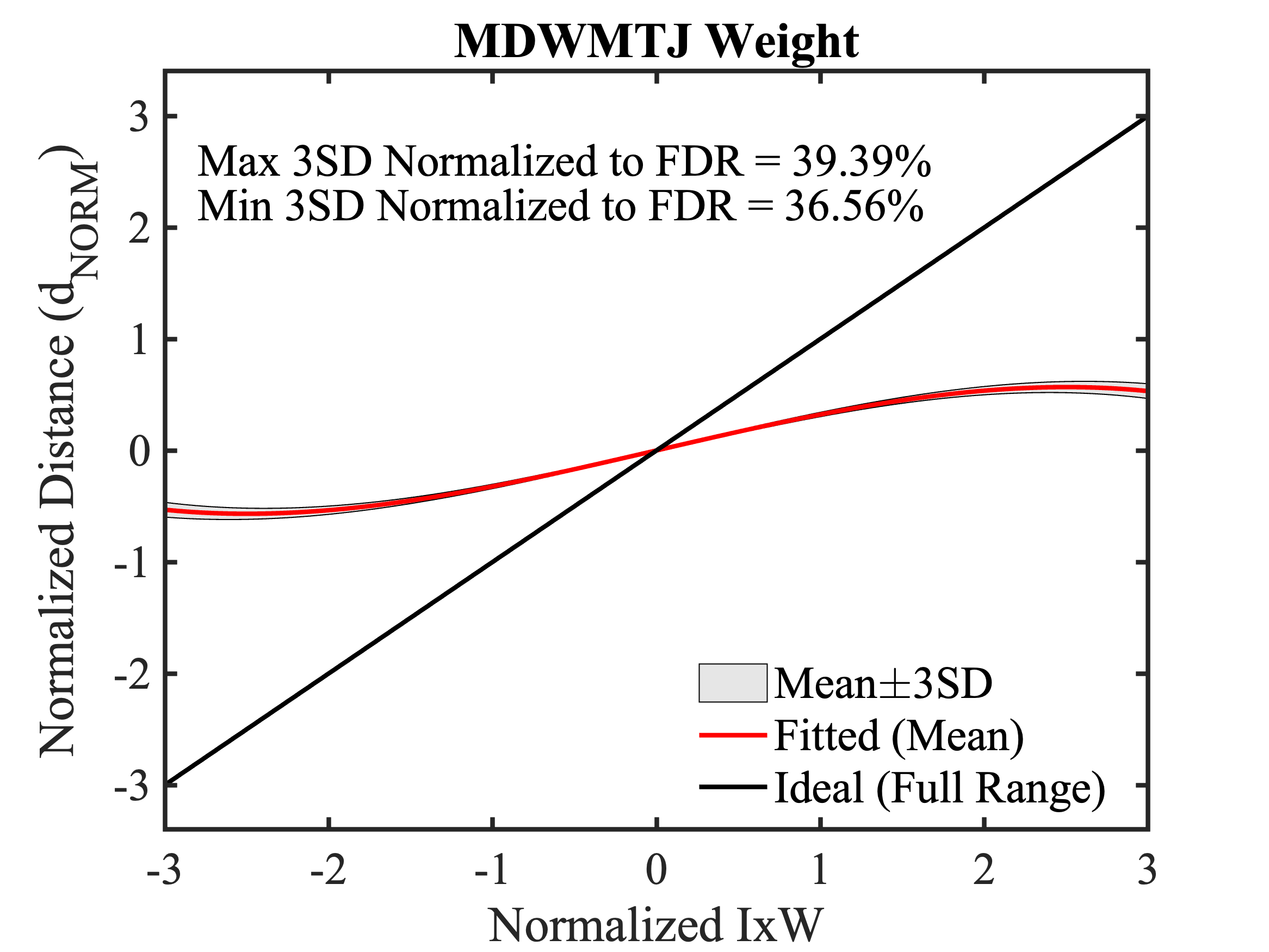
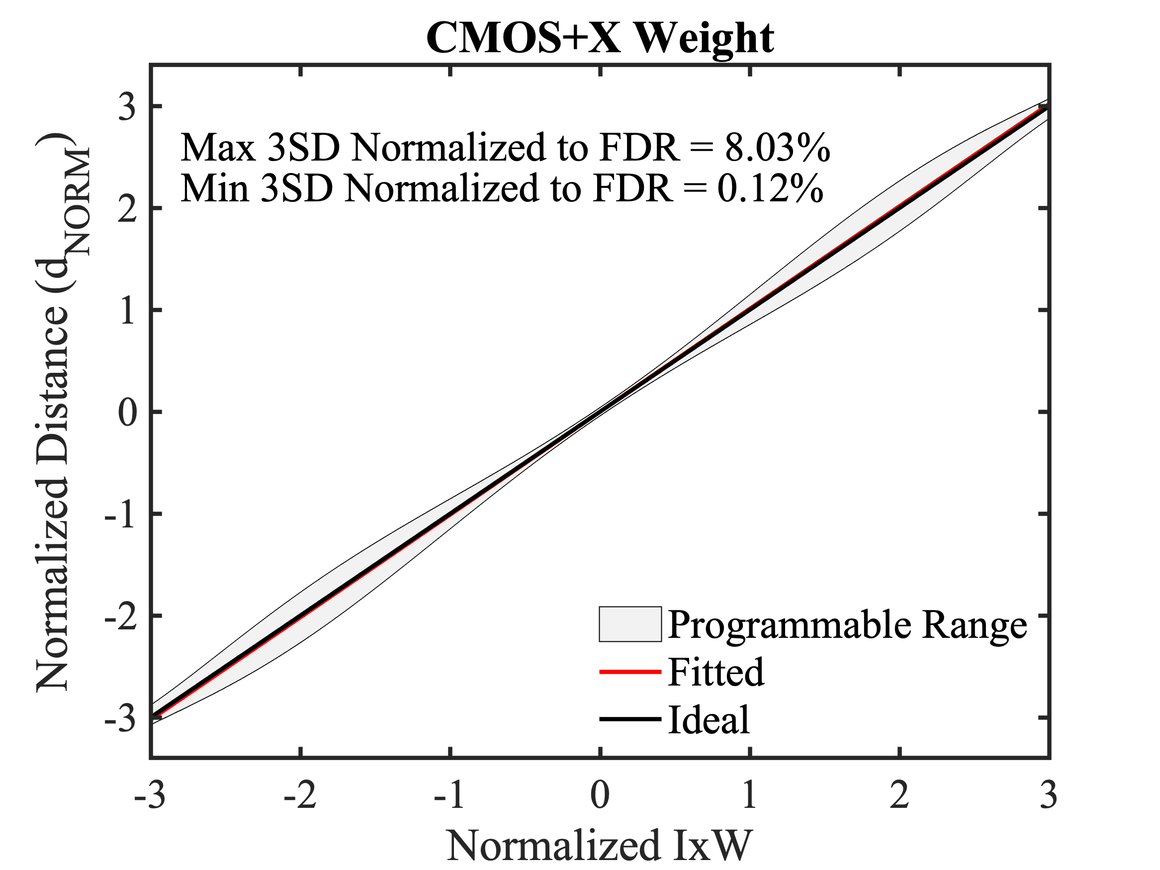
MAC output Modeling: We encode spiking CNN filter weights as the current through the HM of accumulator MDWMTJs, adjusting the weight transistor’s width or/and weight MDWMTJ’s resistance (DW position). Domain wall motion depends on the write current pulse, exhibiting a non-linear relationship with the current (Figure 1(b)). Moreover, the non-linear and voltage-dependent write current by the transistor or/and MDWMTJ is also affected by process variations, fabrication uncertainty, and noise. Simulating for various input spikes and weight combinations, accounting for 3-sigma variation for GF22nm FD-SOI devices, 20% MDWMTJ resistance variation, and 10% clock jitter in the write pulse, our HSpice results for CMOS-based, MDWMTJ-based, and CMOS+X-based configurations (Figures 6(a), (b), and (c), respectively) are modeled using a behavioral curve-fitting function (). Due to the low dynamic range (DR), the MDWMTJ-based weight exhibits higher worst-case variation (39.39%) compared to the CMOS (10.94%) and CMOS+X (8.03%) weights normalized to full DR. The CMOS+X configuration reports a 30-40% normalized programmable range for most weights.
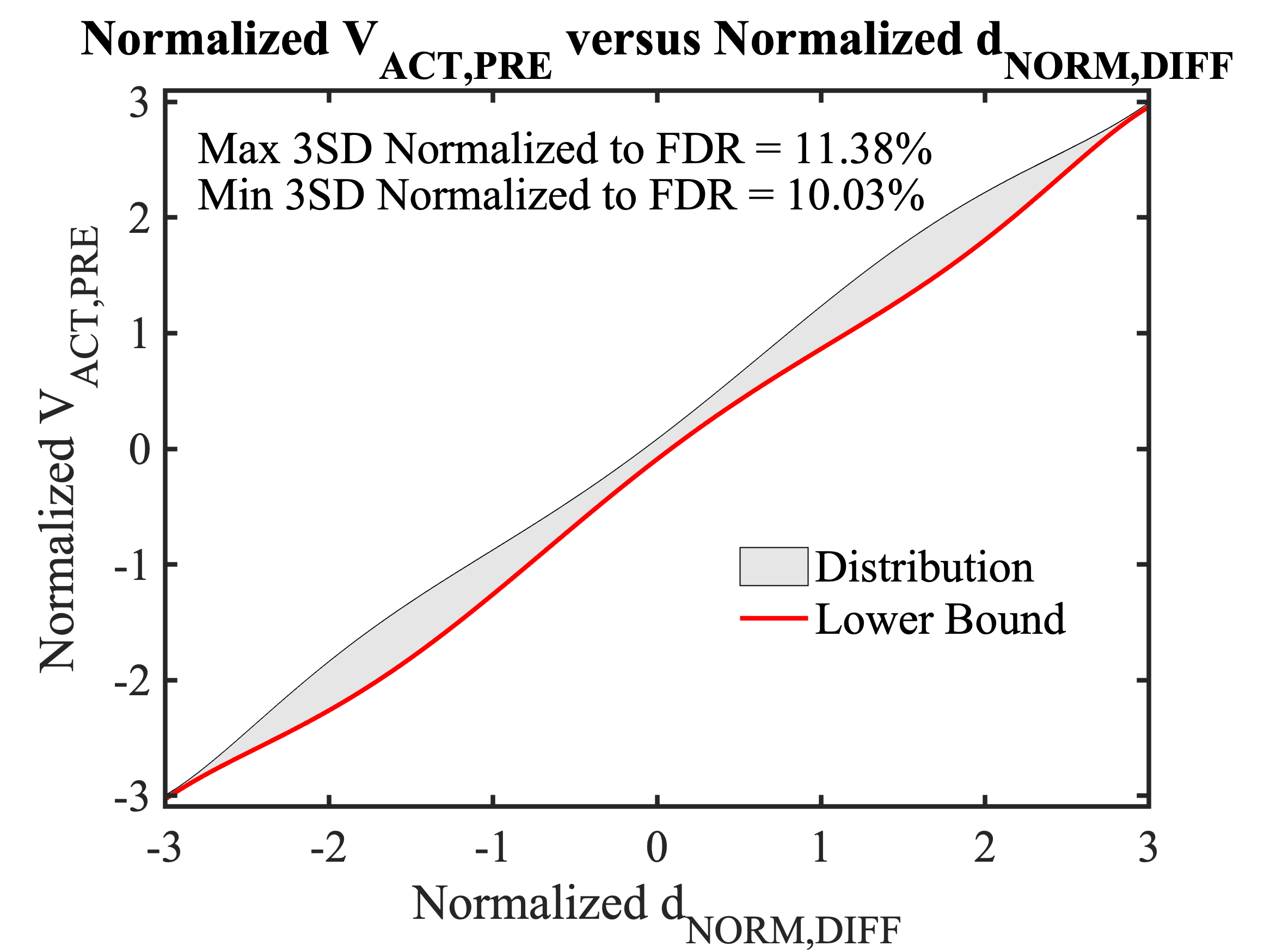
Pre-activation result modeling: After accumulating the DW motion for a fixed integration time, the pre-activation voltage is generated from the series division of the negative and positive accumulator MDWMTJs, where the subtracted outcome (positive MAC output - negative MAC output) non-linearly influences the output voltage of the series divider. Due to the non-linearity and voltage-dependent resistance of the MDWMTJ, identical differences in MAC results may generate different pre-activation voltages. Addressing this non-linearity through extensive HSpice simulations for various combinations (depicted in Figure 6(d)), we model the worst-case scenario (lower bound) that exhibits a maximum of 11.38% variations, utilizing a behavioral curve-fitting function () for the normalized pre-activation voltage versus the normalized distance difference of the accumulator MDWMTJs.
Circuit-Algorithm co-design optimization: Our algorithmic framework generates random Gaussian sample values based on mean and standard deviation results from HSpice simulations to address process variation effects. The accumulated DW position for each pixel’s event spike is calculated using the function incorporating hardware’s non-ideality, aggregated throughout the integration time, to determine MAC results for positive and negative weights. The normalized pre-activation voltage is computed through the function to incorporate the non-linearity and variations of the read circuits. The worst-case scenario (lower bound) is used for pre-activation voltage calculation to ensure accurate output spike generation. This algorithmic framework, employing custom functions and , optimizes spiking CNN training for event-driven neuromorphic datasets. In addition, our algorithmic framework is also optimized utilizing 32 channels with stride 2 for the first layer, ensuring no area overhead for our P2M core.
Device-Algorithm co-design optimization: Due to the limited TMR, our hybrid CMOS+X P2M configuration offers a programmability range 30-40% from its median value. We employ weight tunability restrictions in our algorithmic framework to accommodate diverse applications, enabling our hardware to cater to various applications. Our approach involves initially training weights for one application and subsequently retraining them, considering the normalized weight tunability range derived from HSpice simulation results for another application. Additionally, we leverage kernel-dependent adjustments to neuron thresholds to optimize the algorithmic accuracy.
5 Experimental Results
In this work, we explore and benchmark our proposed neuromorphic CMOS+X P2M solution utilizing the event-driven neuromorphic tasks, specifically classifying video samples captured by NVS cameras. The evaluation is conducted on three widely used neuromorphic benchmark datasets: NMNIST Orchard et al. (2015), CIFAR10-DVS Li et al. (2017), and IBM DVS128-Gesture Amir et al. (2017). The Spikingjelly package Fang et al. (2020) is employed to process and integrate data into fixed time intervals, and a 9:1 train-validation split is applied for these datasets. The spiking CNN architecture consists of four convolutional layers, succeeded by two linear layers featuring 512 and 10 neurons, respectively. Following each convolutional layer, there is a sequence of a batch normalization layer, a spiking LIF layer, and a max pooling layer.
| Dataset | Custom Func. | Noise (%) | Accuracy (%) |
|---|---|---|---|
| NMNIST | No (Baseline) | 0 | 98.10 |
| Yes | 0 | 98.04 | |
| Yes | 10 | 97.82 | |
| Yes | 20 | 97.71 | |
| Yes | 40 | 95.42 | |
| CIFAR10-DVS | No (Baseline) | 0 | 80.72 |
| Yes | 0 | 80.25 | |
| Yes | 10 | 79.17 | |
| Yes | 20 | 77.80 | |
| Yes | 40 | 65.58 | |
| DVS128-Gesture | No (Baseline) | 0 | 97.22 |
| Yes | 0 | 96.53 | |
| Yes | 10 | 95.99 | |
| Yes | 20 | 95.15 | |
| Yes | 40 | 87.25 |
| Train | Evaluate | Fine-tune | Accuracy (%) |
|---|---|---|---|
| CIFAR10-DVS | DVS128-Gesture | No | 9.12 |
| Except layer | 94.96 | ||
| Yes | 96.51 | ||
| DVS128-Gesture | CIFAR10-DVS | No | 10.10 |
| Except layer | 76.73 | ||
| Yes | 80.14 |
5.1 Classification Accuracy & Programmablity
Our spiking CNNs with in-pixel processing achieve test accuracy comparable to SNNs processed with traditional digital hardware (baseline), as demonstrated in Table 1. This success is attributed to the non-volatility of MDWMTJ and our algorithmic optimization considering variations. Additionally, our CMOS+X approach allows re-programmability, enabling post-fabrication tuning of the first layer weights in our P2M hardware for diverse neuromorphic applications. As indicated in Table 2, fine-tuning, especially of the first layer, is essential for maintaining accuracy when transitioning from training on the DVS-CIFAR10 or IBM DVS128-Gesture datasets to other applications. The absence of this fine-tuning results in a significant accuracy drop.
5.2 Details of Bandwidth & Energy Savings
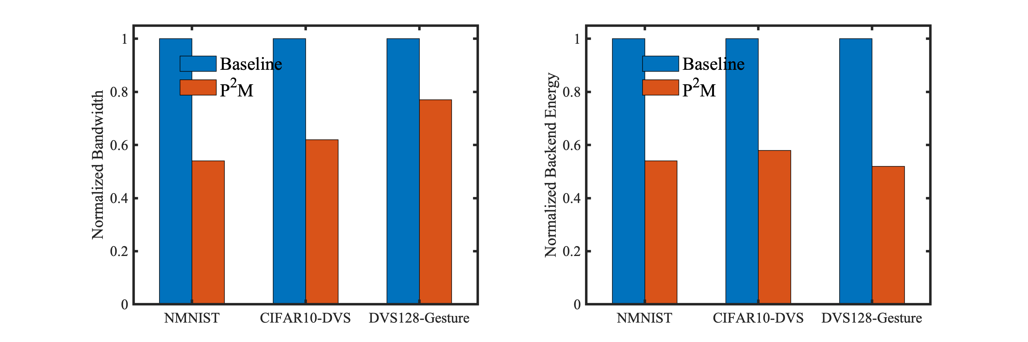
Fig. 7 demonstrates the bandwidth and energy savings with our in-pixel processing approach for the three neuromorphic datasets. We calculate bandwidth as the ratio of average output activation spikes to input event spikes per input sample. To reduce the bandwidth, we employ the bit-level regularizer in the first layer, similar to Sekikawa et al. (2023). The normalized bandwidth reductions of our approach compared to the baseline, where the input spikes are directly sent to the backend processor, are 0.54, 0.62, and 0.77 for NMNIST, DVS-CIFAR10, and IBM DVS128-Gesture, respectively. The backend compute energy consumption is normalized with respect to the conventional backend processing (i.e., digital implementation). Due to the in-pixel processing of the first spiking CNN layer in the analog domain, our approach yields an average (across 3 NVS datasets) of 45.3% lower backend energy. Note that the backend energy is determined by the number of spikes generated by each layer and the memory access of the weights and membrane potential, similar to Yin et al. (2023).
6 Conclusion
We have proposed and implemented a novel CMOS+X processing-in-pixel-in-memory paradigm for neuromorphic event-based sensors. To our knowledge, this is the first CMOS+X implementation proposal for in-pixel processing focusing on neuromorphic vision sensor applications. Leveraging the non-volatility and programmable features of the MDWMTJ and the high dynamic range achieved by the CMOS transistors, our developed spiking CNN hardware can cater to various applications, yielding SOTA accuracy. In addition, we optimize and evaluate our system, incorporating device and circuit constraints into our algorithmic framework based on extensive HSpice simulations. Our neuromorphic CMOS+X P2M-enabled spiking CNN model yields an accuracy of 97.82%, 79.17%, and 95.99% on the NMNIST, CIFAR10-DVS, IBM DVS128-Gesture datasets, respectively and achieved an average of 45.3% backend energy reduction compared to the conventional system.
References
- Chai [2020] Yang Chai. In-sensor computing for machine vision, 2020.
- Eki et al. [2021] Ryoji Eki et al. A 1/2.3 inch 12.3 mpixel with on-chip 4.97 tops/w cnn processor back-illuminated stacked cmos image sensor. In ISSCC 2021, volume 64, pages 154–156. IEEE, 2021.
- Lefebvre et al. [2021] Martin Lefebvre et al. A 0.2-to-3.6 tops/w programmable convolutional imager soc with in-sensor current-domain ternary-weighted mac operations for feature extraction and region-of-interest detection. In ISSCC 2021, volume 64, pages 118–120. IEEE, 2021.
- Tabrizchi et al. [2023] Sepehr Tabrizchi et al. Appcip: Energy-efficient approximate convolution-in-pixel scheme for neural network acceleration. IEEE Journal on Emerging and Selected Topics in Circuits and Systems, 13(1):225–236, 2023.
- Datta et al. [2022a] Gourav Datta et al. A processing-in-pixel-in-memory paradigm for resource-constrained tinyml applications. Scientific Reports, 12, 2022a.
- Hsu et al. [2022] Tzu-Hsiang Hsu et al. A 0.8 v intelligent vision sensor with tiny convolutional neural network and programmable weights using mixed-mode processing-in-sensor technique for image classification. In ISSCC 2022, volume 65, pages 1–3. IEEE, 2022.
- Lichtsteiner et al. [2008] Patrick Lichtsteiner et al. A 128x128 120 db 15 s latency asynchronous temporal contrast vision sensor. IEEE JSSC, 43(2):566–576, 2008.
- Leñero-Bardallo et al. [2011] Juan Antonio Leñero-Bardallo et al. A 3.6 s latency asynchronous frame-free event-driven dynamic-vision-sensor. IEEE JSSC, 46(6):1443–1455, 2011.
- Chen et al. [2020] Guang Chen et al. Event-based neuromorphic vision for autonomous driving: A paradigm shift for bio-inspired visual sensing and perception. IEEE Signal Processing Magazine, 37(4):34–49, 2020.
- Nguyen et al. [2019] Anh Nguyen et al. Real-time 6dof pose relocalization for event cameras with stacked spatial lstm networks. In CVPR, pages 0–0, 2019.
- Maqueda et al. [2018] Ana I Maqueda et al. Event-based vision meets deep learning on steering prediction for self-driving cars. In IEEE CVPR, pages 5419–5427, 2018.
- Datta et al. [2022b] Gourav Datta et al. Can deep neural networks be converted to ultra low-latency spiking neural networks? In DATE 2022, volume 1, pages 718–723, 2022b.
- Song et al. [2022] Ruibing Song et al. A reconfigurable convolution-in-pixel cmos image sensor architecture. IEEE Transactions on Circuits and Systems for Video Technology, 32(10):7212–7225, 2022.
- Zhang et al. [2022] Xueyong Zhang et al. A 915–1220 tops/w, 976–1301 gops hybrid in-memory computing based always-on image processing for neuromorphic vision sensors. IEEE JSSC, 58(3):589–599, 2022.
- Hsu et al. [2020] Tzu-Hsiang Hsu et al. A 0.5-v real-time computational cmos image sensor with programmable kernel for feature extraction. IEEE JSSC, 56(5):1588–1596, 2020.
- Kaiser et al. [2023] Md Abdullah-Al Kaiser, Gourav Datta, Zixu Wang, Ajey P Jacob, Peter A Beerel, and Akhilesh R Jaiswal. Neuromorphic-p2m: processing-in-pixel-in-memory paradigm for neuromorphic image sensors. Frontiers in Neuroinformatics, 17:1144301, 2023.
- Roy et al. [2020] Kaushik Roy et al. In-memory computing in emerging memory technologies for machine learning: An overview. In DAC 2020, pages 1–6. IEEE, 2020.
- Ankit et al. [2017] Aayush Ankit et al. Resparc: A reconfigurable and energy-efficient architecture with memristive crossbars for deep spiking neural networks. In DAC 2017, pages 1–6, 2017.
- Sengupta et al. [2016] Abhronil Sengupta et al. Proposal for an all-spin artificial neural network: Emulating neural and synaptic functionalities through domain wall motion in ferromagnets. TBioCAS, 10(6):1152–1160, 2016.
- Leonard et al. [2022] Thomas Leonard et al. Shape-dependent multi-weight magnetic artificial synapses for neuromorphic computing. Advanced Electronic Materials, 8(12):2200563, 2022.
- Alamdar et al. [2021] Mahshid Alamdar et al. Domain wall-magnetic tunnel junction spin-orbit torque devices and circuits for in-memory computing. APL, 118(11), 2021.
- Ikeda et al. [2008] S Ikeda et al. Tunnel magnetoresistance of 604% at 300k by suppression of ta diffusion in cofeb/ mgo/ cofeb pseudo-spin-valves annealed at high temperature. APL, 93(8), 2008.
- Hu et al. [2019] Xuan Hu et al. Spice-only model for spin-transfer torque domain wall mtj logic. IEEE TED, 66(6):2817–2821, 2019.
- Wang et al. [2020] Chao Wang et al. Compact model of dzyaloshinskii domain wall motion-based mtj for spin neural networks. IEEE TED, 67(6):2621–2626, 2020.
- Wang et al. [2021] Manman Wang et al. Compact model of domain wall mtj driven by spin-orbit torque and dzyaloshinskii–moriya interaction. IEEE Transactions on Magnetics, 58(8):1–5, 2021.
- Martinez et al. [2014] Eduardo Martinez et al. Current-driven dynamics of dzyaloshinskii domain walls in the presence of in-plane fields: Full micromagnetic and one-dimensional analysis. Journal of Applied Physics, 115(21), 2014.
- Luo et al. [2021] Shijiang Luo et al. Integrator based on current-controlled magnetic domain wall. APL, 118(5), 2021.
- Fong et al. [2011] Xuanyao Fong et al. Knack: A hybrid spin-charge mixed-mode simulator for evaluating different genres of spin-transfer torque mram bit-cells. In 2011 International Conference on Simulation of Semiconductor Processes and Devices, pages 51–54. IEEE, 2011.
- Miura et al. [2019] Tsukasa Miura et al. A 6.9 m pixel-pitch 3d stacked global shutter cmos image sensor with 3m cu-cu connections. In 3DIC 2019, pages 1–2. IEEE, 2019.
- Kagawa et al. [2020] Y Kagawa et al. Impacts of misalignment on 1m pitch cu-cu hybrid bonding. In IITC 2020, pages 148–150. IEEE, 2020.
- Boahen [2004] Kwabena A Boahen. A burst-mode word-serial address-event link-i: Transmitter design. IEEE TCAS-I, 51(7):1269–1280, 2004.
- Zhu et al. [2020] Daoqian Zhu et al. Threshold current density for perpendicular magnetization switching through spin-orbit torque. Physical Review Applied, 13(4):044078, 2020.
- Orchard et al. [2015] Garrick Orchard et al. Converting static image datasets to spiking neuromorphic datasets using saccades. Frontiers in Neuroscience, 9, 2015. URL https://www.frontiersin.org/articles/10.3389/fnins.2015.00437.
- Li et al. [2017] Hongmin Li et al. Cifar10-dvs: An event-stream dataset for object classification. Frontiers in Neuroscience, 11, 2017. URL https://www.frontiersin.org/articles/10.3389/fnins.2017.00309.
- Amir et al. [2017] Arnon Amir et al. A low power, fully event-based gesture recognition system. In CVPR 2017, volume 1, pages 7388–7397, 2017.
- Fang et al. [2020] Wei Fang et al. Spikingjelly, 2020.
- Sekikawa et al. [2023] Yusuke Sekikawa et al. Bit-pruning: A sparse multiplication-less dot-product. In The Eleventh International Conference on Learning Representations, 2023. URL https://openreview.net/forum?id=YUDiZcZTI8.
- Yin et al. [2023] R Yin et al. Sata: Sparsity-aware training accelerator for spiking neural networks. IEEE Transactions on Computer-Aided Design of Integrated Circuits and Systems, 42(6):1926–1938, 2023.