Thermal-Aware Floorplanner for 3D IC, including TSVs, Liquid Microchannels and Thermal Domains Optimization
Abstract
3D stacked technology has emerged as an effective mechanism to overcome physical limits and communication delays found in 2D integration. However, 3D technology also presents several drawbacks that prevent its smooth application. Two of the major concerns are heat reduction and power density distribution. In our work, we propose a novel 3D thermal-aware floorplanner that includes: (1) an effective thermal-aware process with 3 different evolutionary algorithms that aim to solve the soft computing problem of optimizing the placement of functional units and through silicon vias, as well as the smooth inclusion of active cooling systems and new design strategies,(2) an approximated thermal model inside the optimization loop, (3) an optimizer for active cooling (liquid channels), and (4) a novel technique based on air channel placement designed to isolate thermal domains have been also proposed. The experimental work is conducted for a realistic many-core single-chip architecture based on the Niagara design. Results show promising improvements of the thermal and reliability metrics, and also show optimal scaling capabilities to target future-trend many-core systems.
keywords:
3D architecture , Thermal-aware floorplan , Air channels , Through silicon vias , Evolutionary algorithmsGlossary
- AC
- Air Channel
- DVFS
- Dynamic Voltage and Frequency Scaling
- FU
- Functional Unit
- IC
- Integrated Circuit
- LC
- Liquid Channels
- MFA
- Multi-objective Floorplanning Algorithm
- MOEA
- Multi-Objective Evolutionary Algorithm
- PCB
- Printed Circuit Board
- RC
- Resistance-Capacitance
- TSV
- Through Silicon Via
1 Introduction
The process of continuous scaling over the past decades has led to important improvements in size and performance of electronic products, but it has also led to several challenges such as communication problems and temperature management.
The shift to the many-core architectures has been driven by the advances in semiconductor technologies. Besides, the increase in power dissipation has been tailored by dynamic techniques like Dynamic Voltage and Frequency Scaling (DVFS) [Choi2002], using several clock domains [Ogras2007] or task migration policies [Cuesta2010]. These techniques, however, may also impact negatively the performance of the system. Design-time approaches like the one proposed in this paper are able to mitigate the effect of high temperatures and, also, are compatible with any other existing dynamic technique applied to maintain or even increase the performance of the system.
One important mechanism to overcome physical limits in Integrated Circuit (IC) design underlies on the design of multi-level ICs using advanced processes. These techniques boost the concept of three dimensional integrated circuits (3D ICs). 3D designs improve the performance of the system by reducing interconnect delays and increasing the density of the logic. Through Silicon Vias (TSVs) connect multiple layers of the stack reducing distances between Functional Units (FUs), hence decreasing the communication delay. This fabrication technology also allows the integration of multiple and disparate technologies, such as radio frequency and mixed signal components, with traditional computing technologies.
However, 3D integration exacerbates the problem of temperature in the chip, specially temperature in inner layers. These thermal problems are increasingly affecting the performance and the reliability of electronic systems. [Shang2004] reported that over 50% of electronic product failures are caused by thermal issues and the presence of hotspots. Increasing the temperature decreases lifetime of the chip exponentially. Furthermore, higher temperature can cause slower devices, can increase leakage current, and can reduce the performance due to the impact in the metal resistivity.
Considering these facts, it is desired to keep the components and the chip structure as cool as possible for maximum reliability. However, the absolute temperature of the chip is not the only factor that affects performance; moreover, the thermal gradients that appear on the chip surface degrade the system reliability through the promotion of dangerous electro-migrations [Jonggook:TemperatureGradient:99].
One way in which hardware designers have tried to address the thermal problem is with the use of thermal-aware floorplanners such as [Cong2004] (that proposed a thermal-driven floorplanning algorithm for 3D ICs) or [Healy2007] (where the authors implemented a multi-objective floorplanning algorithm for 2D and 3D ICs, combining linear programming and simulated annealing). Some other authors have also considered the placement of thermal vias in these 3D stacks to optimize the thermal profile of ICs [Wong2006]. The careful placement of active modules in a 3D stack can optimize the wire length that connects FUs by reducing the communication delays, and can also provide a homogeneous temperature distribution across the chip. Apart from static approaches of thermal optimization, dynamic techniques are required to manage the high power densities found in these architectures. While the conventional air cooling has proved to be insufficient for 3D-ICs, the interlayer micro-channel liquid cooling provides a better option to address this problem. Some works like [DelValle2010] and [Coskun2009] have focused in thermal modeling with active cooling. These works have studied the effect of allocating liquid channels between active layers and their cooling effect.
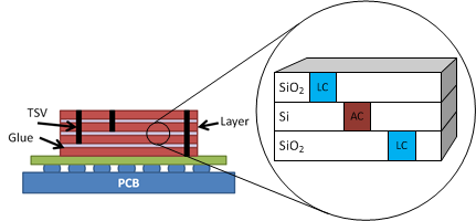
Some of the goals in the design of 3D stacks are to achieve a reduction in area and also to decrease the length of the interconnections, that would be translated into improved data transfer times and power consumption. Figure 1 summarizes our proposed concept of a 3D-IC architecture. Based on [Sabry2011], the 3D stack is built over a Printed Circuit Board (PCB), which is considered to be adiabatic. Then, several layers are stacked, as can be seen in Figure 1. Every layer of the stack is composed of silicon and silicon dioxide. Liquid Channelss (LCs) is used as an active cooling system. These channels are placed in the silicon dioxide just over the active layers. Liquid channels absorb heat produced by FUs with a high power density, reducing the temperature of inner layers. LCs contain a coolant (generally water) that is pumped into the chip. In this paper we also propose a novel architectural set-up based on isolation channels or Air Channels (ACs). Air channels are etched in silicon and filled with low pressure air. Since heat spread is mainly diffusive, air channels prevent cold areas to be affected by the power dissipated in other regions of the chip, creating temperature domains or regions. The use of air channels has the major purpose of isolating thermal regions. This could seem counter intuitive as the heat flow from hotter modules could not be dissipated by the cooler ones. However, the idea behind this is the optimization of the active cooling mechanism (liquid channels), whose placement, number and required cooling energy are benefited by the air channels. More in detail:
-
1.
Since the chip is split in several independent regions, the thermal distribution of every domain can be defined attending to design constraints. In this way, it is easier to obtain a homogeneous distribution, or a pattern of alternate warm and cold regions, that help on achieving a more controlled thermal profile in the design phase.
-
2.
If high temperatures are located in certain regions, dissipation mechanisms can be applied in those areas where the thermal problems are exacerbated, minimizing technological costs and optimizing the cooling properties of the different techniques.
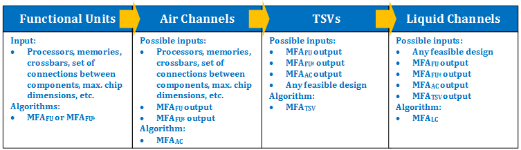
All this architectural diversity encourages the research on the design of optimization algorithms to place automatically FUs, TSVs, as well as liquid and air channels, minimizing maximum temperature and total wire length. The efficient management of all these input variables, and the multiple optimization criteria given by several objectives that have to be accomplished at the same time, requires innovative algorithms capable of evaluating all these parameters and returning the best set of solutions. In the case of 3D IC design, incremental optimization is a promising way to handle multi-objective optimization with complicated constraints and to facilitate the design reuse technology. Many works have been published with this approach, however, none took into account thermal-aware floorplanning. Most multi-objective floorplanning algorithms in the literature are developed using Genetic Algorithms or Simulated Annealing, where the main problem relies on the formulation of the representation. Common representations for the floorplanning problem are polish notation [Berntsson2004], combined bucket array [Cong2004] and O-tree [Tang2007]. Most of these representations do not perform well in our scenario because they were initially developed to reduce area, whereas our problem is based on minimizing temperature. To this end, we extend in this paper our previous algorithm for floorplanning optimization named Multi-objective Floorplanning Algorithm (MFA) [Cuesta2013], in which we formulated a multi-objective optimization problem for 3D thermal aware floorplanning that is able to reduce peak temperature, eliminate hotspots, and hence decrease reliability risks related to temperature. MFA allows the incremental placement of FUs and TSVs.
In this paper, we will denote this algorithm with MFA . From our previous work in [Cuesta2013], as Figure 2 introduces, we have enhanced the TSVs placement developing the new MFA that slightly extends MFA to obtain solutions where at least one TSV configuration can be reached. We have also developed two new evolutionary algorithms. These algorithms solve the integration of active cooling systems within the 3D IC using liquid channels by optimizing their placement in those areas where the temperature is higher. The second new algorithm can manage the optimization of FU and TSV in the 3D IC design with air channels, taking into account new placement restrictions in the model. Results show that the inclusion of isolation channels creates temperature regions, decreasing the energy overhead imposed by the active cooling system.
This paper makes major contributions in the area of thermal optimization in 3D-integrated circuits. As compared with previous approaches, the work presented here achieves a practical and effective solution in the field of interest, outperforming the results obtained by these works. This paper also extends our previous work presented in [Cuesta2013] with the following major upgrades:
-
1.
The proposal of a novel structure, called air isolation channels, as an effective mechanism for thermal isolation in 3D chips.
-
2.
The development of the required thermal models for these structures that enable their control by the optimization algorithm.
-
3.
The extension of the MFA algorithm presented in [Cuesta2013] with two new evolutionary algorithms, to consider the new design constraints and technologies, achieving better results in terms of thermal profile and fabrication costs.
The rest of the paper is structured as follows: Section 2 describes both the thermal model and current implementation of MFA. Then, Section 3 continues with an explanation of the proposed optimizer. The experimental set-up used for our scenario is then described in Section LABEL:sec:SetUp and finally, results and conclusions are presented in Sections LABEL:sec:Results and LABEL:sec:conclusions, respectively.
2 Thermal model
The equation governing heat diffusion via thermal conduction in a 3D stack is [Brooks2007]:
| (1) |
subject to the boundary condition
| (2) |
Regarding Equation 1, is the material density, is the mass heat capacity, and are the temperature and thermal conductivity of the material at position and time , and is the power density of the heat source. With respect to Equation 2, is the outward direction normal to the boundary surface , is the heat transfer coefficient and is an arbitrary function at the surface .
Numerical thermal analysis can be accomplished by applying a seven points finite difference discretization method to Equation 1, which decomposes the 3D stack into numerous rectangular parallelepipeds of non-uniform sizes and shapes if necessary. In this way, each element has a power dissipation, temperature, thermal capacitance and thermal resistance to adjacent elements, which interact via heat diffusion. The discretized equation at an inner point of a grid element is:
| (3) | |||||
where , and are discrete offsets along the , and axes, is the discretization step in time , , and are discretization steps along the , and axes, and . Finally, , and are the thermal conductivities between adjacent elements, defined as follows: , , and .
For a 3D stack with discretized elements, equation 3 can be summarized as follows:
| (4) |
where the thermal capacitance matrix is an diagonal matrix, the thermal conductivity matrix is an sparse matrix, and are temperature and power vectors, and is the unit step function.
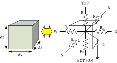
Equation (4) can be characterized by a 3D Resistance-Capacitance (RC) model as the one presented in [Ayala2012]. Voltage differences are analogous to temperature differences, and the electrical resistance is analogous to thermal resistance. The thermal modeling of the stack in Figure 1 can be performed splitting the chip into small cubic unitary cells.
Silicon and silicon dioxide cells are modeled with six thermal resistances and one thermal capacitance as it can be seen in Figure 3. Four of these resistances connect each cell to its lateral neighbors (those on the same layer), while the two remaining resistances connect the cell with the upper and bottom cell, respectively. The capacitance represents the heat storage inside the cell.
Air channels also have a diffusive behavior. Despite the fact air is a fluid, the dimensions of the cavity and the absence of forced convection methods, make the fluid to behave as a diffusive material. We have considered channels fabricated and filled with low pressure air, which decreases thermal conductivity, making isolation much more efficient.
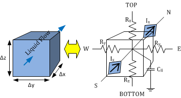
Liquid channels are electrically modeled as it can be seen in Figure 3. This difference with the diffusive cell comes because, in cells circulating a coolant, the mechanism that dominates the heat transfer is the forced convection. This mechanism can be translated into our RC model using two voltage controlled current sources, as it is profusely covered in [Sridar2010].
Heat diffusion to the surrounding environment is also considered by the RC model. This diffusion occurs in the edge of the chip and in the top layer. Different chip packages and heat sinks can be integrated in Equation (4) by tuning the capacitance and resistance parameters of the model. As the PCB base is considered to be adiabatic, no heat transfer occurs in the bottom direction of the first layer.
The interface material that exists in between two silicon layers, used as a glue, is modeled as an epoxy layer, a pure resistant material. The existence of TSVs is considered in the model, also as a resistance element.
| Si linear thermal conductivity | 295 W/(mK) |
|---|---|
| Si quadratic term of thermal conductivity | -0.491 W/(m) |
| SiO thermal conductivity | 1.38 W/(mK) |
| Si specific heat | 1.628 x J/K |
| SiO specific heat | 4.180 x J/K |
| Epoxy specific heat | 1.73 x J/K |
| Epoxy thermal conductivity | 0.03 W/(mK) |
| TSV thermal conductivity | 372 W/(mK) |
| TSV specific heat | 3.45 x J/K |
| Isolating Air thermal conductivity | 2.4 x W/(mK) |
| Isolating Air specific heat | 1 x J/K |
| Water specific heat | 4.184 x J/K |
| Water thermal conductivity | 0.58 W/(mK) |
| Stack width | 12000 m |
|---|---|
| Stack length | 10500 m |
| Cell size (lxw) | 300x300 m |
| TSV cell size (lxw) | 300x300 m |
| Liquid channel width | 300 m |
| SiO height | 50 m |
| Si height | 150 m |
| Epoxy height | 25 m |
3 Design Flow: Multi-objective Floorplanning Algorithm
MFA was first proposed by David Cuesta et al. [Cuesta2013]. This algorithm performs an incremental floorplanning divided in two phases. First, FUs are placed by running MFA . Secondly, MFA is executed, placing TSVs. These two processes are independent. Thus, MFA tends to obtain floorplans where the insertion of TSVs is not possible. In this section we describe all the algorithms implied in the design flow shown in Figure 2, including these two sub-algorithms for self-content purposes. We also improve MFA to reach feasible solutions for the insertion of TSVs.
3.1 MFA
MFA is a Multi-Objective Evolutionary Algorithm (MOEA) based on NSGA-II [Deb2002]. The foorplanner manages coded solutions that are gradually improved in the evolutionary process to provide configurations optimized both in performance and thermal response for the target architecture. To this end, MFA simultaneously minimizes the following three objectives:
-
1.
: Number of topological constraints violated (overlapping between different blocks, or components out of the borders of the chip).
-
2.
: Wire length, approximated as the Manhattan distance between interconnected blocks :
(5) , where are the coordinates of FU .
-
3.
: Maximum temperature of the chip. The computation of this objective depends on the chosen thermal model. In the case of MFA , the contribution to the maximum temperature of two FUs is simplified as the cross product of their power densities divided by the corresponding euclidean distance. Thus, having FUs, is defined as:
(6) By minimizing the algorithm will try to place hottest blocks as far as possible. This process reduces maximum temperature, as it is demonstrated in [Cuesta2013].
MFA can be classified as a hybrid foorplanning approach because the decoding heuristic implements an incremental foorplanning inspired in constructive techniques, while the MOEA on top of the heuristic is essentially iterative.
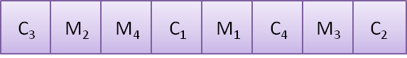
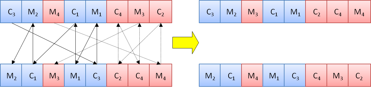
We use a permutation encoding [Sivanandam2007], in which every chromosome is a string of records representing the different FUs of the target architecture. These records gather information relative to a FU, namely label, width, and length. Managing the width and length of the blocks allows to perform rotations, granting further degrees of freedom to the optimization process. Additional characteristics of the FUs such as power densities, connections, etc., must be managed by the algorithm. However, this information does not need to be codified in the chromosomes as it is common to all the individuals. Figure 4 depicts the representation of a chromosome used in MFA . The example shows a candidate solution (individual) of a platform composed of 8 FUs: 4 cores and 4 memories . The order determines the placement sequence. Thus, will be placed first, followed by , and so on.
All the chromosomes must have size , where is the number of FUs to be placed. Therefore, the cardinality of the considered solution space is . The operators designed according to the representation are depicted in Figure 4 and briefly described below:
-
1.
Selection: The selection operator implements a binary tournament strategy. To this end, random couples of individuals are formed and the best solution of each pair is selected for crossover.
-
2.
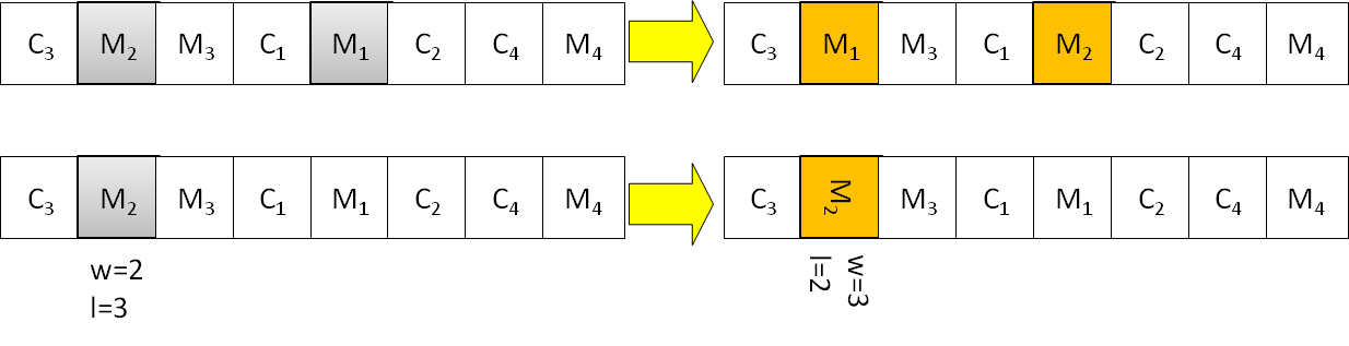
Crossover: A cycle crossover is used to produce the offspring, this operator must take into account that all the components must appear once and only once in the chromosome (see Figure 4).
- 3.
Algorithm 1 shows the implementation of MFA . As Figure 2 indicates, the initial population is built from a list of components to be placed in the floorplan, along with their dimensions and interconnectivity. Each chromosome is defined just as a random sequence of these components (see Figure 4). A heuristic is in charge of the placement of the different elements of the architecture (decoding of the solutions). The heuristic performs an incremental floorplanning in which the components are sequentially placed in the 3D stack following the order implied by the solution encoding. In fact, as the exhaustive heuristic alone is capable of obtaining well performing solutions, the MOEA is designed to obtain the optimal order of the components given the placement heuristic. In this heuristic, every block is placed considering all the topological constraints, the wire length, and the maximum temperature of the chip with respect to all the previously placed blocks , named as . The best location for each block is selected depending on whether the block is a relative heat sink or a heat source. For a heat source (like a core, for example) the best position is the one with lowest to ensure an even thermal distribution. If the block is a heat sink (like a memory) the best position is the one with lowest wire length . With this procedure, the authors try to ensure a correct thermal optimization. This approach is highly reasonable in terms of thermal profile, since large 3D stacks with more than 48 cores reach prohibitive temperatures (more than 400 K, as can be seen in [Cuesta2013]). Thus, every block is fixed in the remaining position . Once the placement has finalized, the obtained configuration is evaluated according to the three defined objectives . In order to help the algorithm to find feasible solutions, the multiobjective function can be transformed to . Although the first objective can be removed in this case, we keep it to easly check if the algorithm is not able to find feasible solutions.
3.2 TSV Optimization: MFA
As aforementioned, this algorithm is responsible of the placement of TSVs to allow vertical communications. As in MFA , MFA is based on NSGA-II. In the original version of MFA, this algorithm is the step executed immediately after MFA . Since TSVs insertion is not checked in the first algorithm, it could happen that MFA did not find a feasible distribution of TSVs. To solve this issue, we improve MFA in the next subsection. In the following, we describe the MFA algorithm.
Technologically, and due to fabrication process constraints, TSVs can only be built from one specific layer to any other. In this regard, MFA considers the top layer as the initial one.
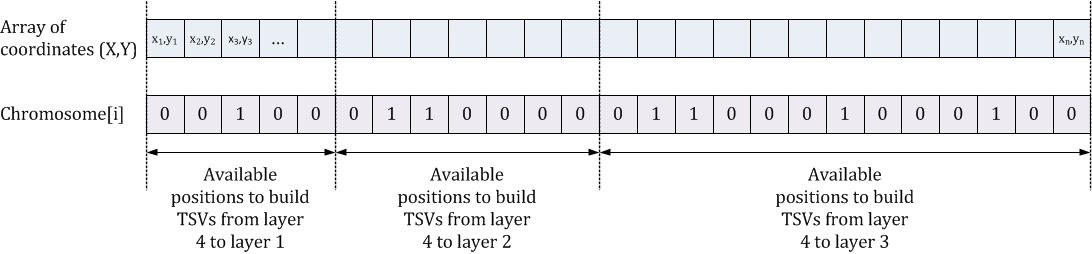
To encode a solution, MFA examines the remaining free cells in the MFA resultant stack. Then, MFA builds an array of x-y coordinates where TSVs can be drilled, as the array of coordinates in Figure 5 shows. Given a 3D IC with layers, a first region of this array contains the coordinates where a TSVs between layers and can be built; a second region in the same array contains the coordinates where TSVs between layers and can be built, and so forth. Next, a 0-1 chromosome of length equal to the array of coordinates is created. If a gene contains a , a TSV is inserted in the corresponding (x,y) position, between the layers that belong to the corresponding region. In this way, Figure 5 encodes TSVs in four layers (): 1 TSV drilled between layers and , TSVs between layers and , and TSVs between layers and . As a result, the initial population is a set of binary chromosomes randomly generated. The corresponding (x,y) coordinates are stored in a separate array of coordinates.
Algorithm 2 shows a pseudocode for MFA . This algorithm returns a set of solutions, considering the number of TSVs and the new total wire length . This set constitutes a Pareto front approximation, and the designer will have the chance to select the best solution in terms of economic cost and wire length reduction, considering that a minimum number of TSVs must be included in the design in order to fulfill the communication constraints. The minimum number of TSVs is calculated attending to the communication bandwidth needs of cores. We have calculated the data that is transferred by an FM modulation/demodulation application as the one explained in [Cuesta2010]. The minimum number of TSVs is given by the technological parameters of the TSVs and the volume of data to transfer [Weldezion2009].
3.3 MFA
In this Section, we slightly modify MFA to obtain solutions where at least one TSV configuration can be reached by MFA . To this end, we present Algorithm 3. We only show the evaluation function because the main function is identical to MFA . The modification is performed including the matrix. contains all the free cells in the 3D stack. Thus, given a floorplan, it is quite easy to check if a TSV can be drilled to connect two blocks placed at different layers. If this is not possible, is set to infinity.
In the following subsections we present two new subalgorithms of MFA, named MFA and MFA . MFA has been developed to place liquid channels in the 3D IC. MFA has been designed to divide the 3D stack into regions isolated by air channels. It is worth noting that the following two algorithms receive as input the resultant 3D IC obtained either by MFA or MFA +MFA