Observation of Surface State Suppression in Magnetic Weyl Semimetal NdAlSi
Abstract
Understanding and mastering the control of surface states in topological materials are crucial steps for the development of future electronic devices and technologies that leverage the unique properties of these materials. Here, using angle-resolved photoemission spectroscopy, we provide a good case study of this by visualizing the electronic structure of a magnetic Weyl semimetal on both flat and uneven surfaces. Our observations reveal that the preparation of an uneven sample surface can effectively suppress all surface states in the Weyl semimetal NdAlSi, including topological surface Fermi arcs. This results in the observation of pure bulk states devoid of any Fermi energy shift. This discovery not only opens up a new avenue to directly study the pure bulk states of a Weyl semimetal using low photon energies in ARPES but also provides key insights into the control of the surface states in topological materials.
Introduction
Surface states are a special electronic states that are confined to the boundary of a crystal, first proposed by Tamm in 1932[1]. Later, Shockley discovered a surface state that can occur in the energy gap caused by the crystal field inversion, which is called the Shockley surface state[2]. More recently, another type of surface state, the topological surface state, has attracted great interest in the condensed matter physics community. The topological surface states are unique electronic states that exist at the surface of topological insulators[3, 4] or topological semimetals[5, 6, 7]. The existence of surface states in materials, especially topological surface states, can cause some unique physical phenomena, such as the anomalous[8, 9, 10] and spin Hall effect[11, 12], and chiral anomalous charge[5, 6, 7]. In the last decade, angle-resolved photoemission spectroscopy (ARPES) has been used extensively to study topological materials and their surface states[3, 4, 5, 6, 7]. When employing ARPES to investigate the electronic structure of topological materials, a common challenge is that the electronic structures of surface and bulk states tend to overlap, particularly in Weyl semimetals. To address this issue and directly examine the properties of bulk states, measurements often utilize the bulk sensitivity of soft X-rays ARPES, leading to lower energy resolution. In this context it would be advantageous if surface states could be entirely suppressed while preserving the integrity of the bulk states. Achieving complete suppression of surface states through controlled manipulation also holds significant promise for engineering applications[13]. However, simultaneously avoiding any noticeable impact on the bulk states, including no Fermi energy shift, presents a notable challenge.
Here, we provide a case study showing that it is possible to completely suppress all surface states in a Weyl semimetal, even topological surface states, by preparing an uneven crystal surface, resulting in the observation of pure bulk states without any noticeable Fermi energy shift. In this work, employing ARPES measurements and density functional theory (DFT) calculations, we systematically investigate the electronic structure of the magnetic Weyl semimetal NdAlSi on both flat and uneven surfaces. Our findings reveal that the electronic structure measured on the flat surface predominantly originates from the surface states, while the electronic structure measured on the uneven surface is attributed to the bulk states. Notably, trivial surface states and surface Fermi arcs are entirely suppressed on the uneven surface of NdAlSi, with no discernible Fermi energy shift of the bulk states. The temporal evolution of the electronic structure suggests that the phenomenon of suppressing trivial surface states on uneven surfaces may be linked to the easier saturation of dangling bonds associated with trivial surface states compared to flat surfaces. Our results not only offers a pathway to directly measure pure bulk states using low photon energies in ARPES but also provides crucial insights into the control of surface states in topological materials.
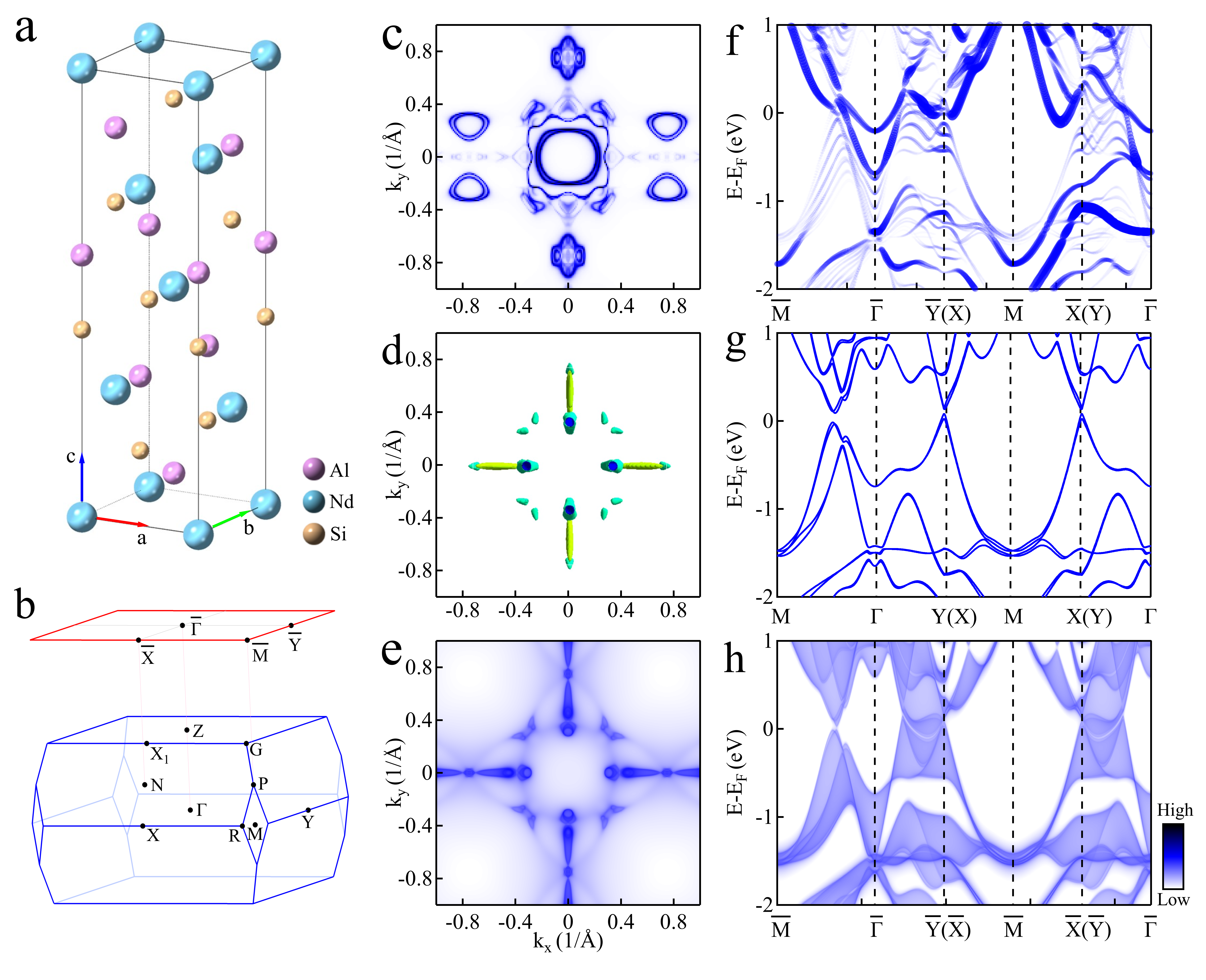
Figure 1a shows the crystal structure of NdAlSi, which crystallizes in the tetragonal structure with the space group I41md (no. 109)[14]. The corresponding three-dimensional (3D) Brillouin zone (BZ) of NdAlSi is shown in Fig. 1b, which defines the high symmetry points in the BZ. According to previous reports, the Al-Nd layer is the dominating cleavage plane in NdAlSi[15, 16]. DFT calculations predict that the Nd terminated surface from a cleave at the Al-Nd layer forms a complex surface state (Fig. 1c and 1f) which differs from the electronic structure of the bulk state (Fig. 1d and 1g)[15]. Furthermore, DFT calculations of the bulk states, integrated along the kz direction as shown in Fig. 1e and 1h, provide an overall understanding of the bulk versus surface electronic structure of NdAlSi.
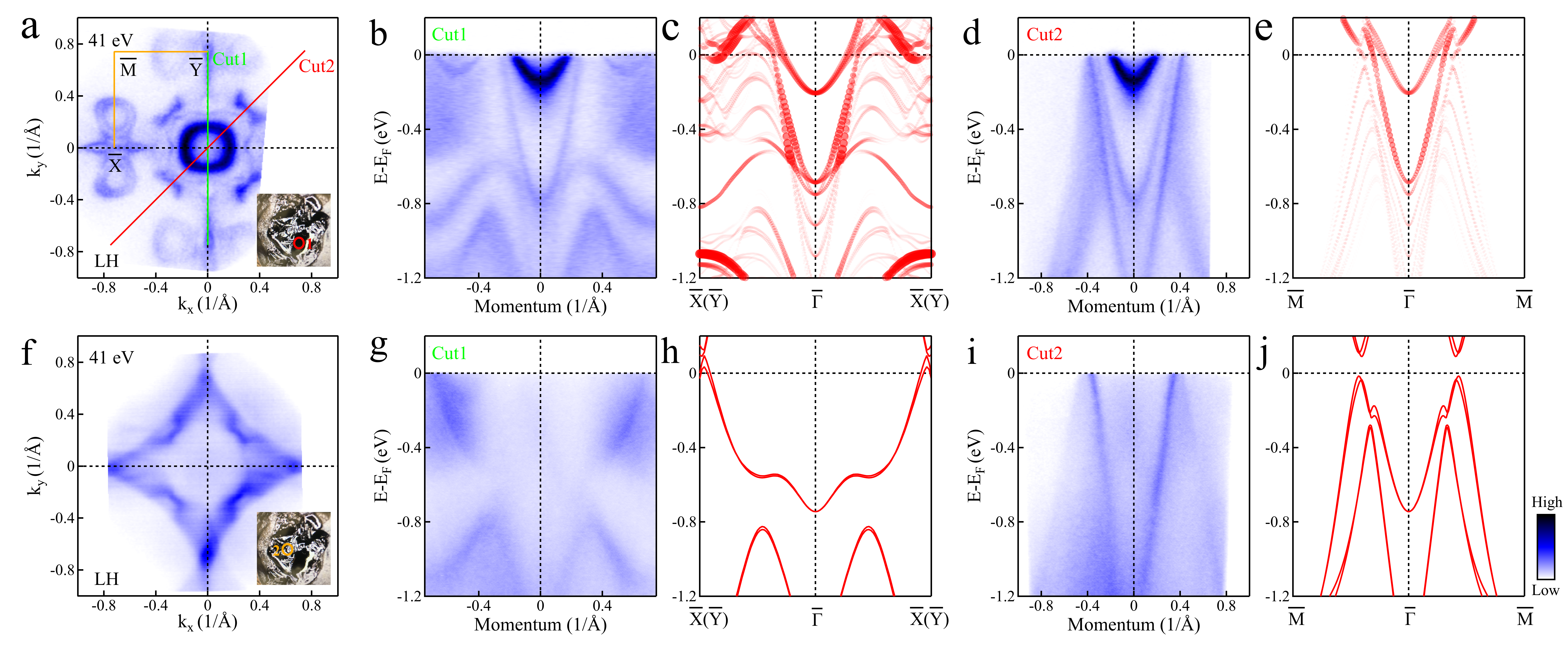
Concurrently with DFT calculations, we performed ARPES measurements on NdAlSi. Since NdAlSi is a 3D non-centrosymmetric crystal, the single crystal after cleavage shows flat areas (area 1 in Fig. 2a) as well as areas with multiple steps (area 2 in Fig. 2f). The corresponding location can be found by spatial scanning of the sample. When the measurement position is in area 1 (red circle in Fig. 2a), the measured Fermi surface is as shown in Fig. 2a. It is seen that the measured Fermi surface (Fig. 2a) is in good agreement with the surface projected DFT Fermi surface calculations for the Nd terminated surface at the Al-Nd layer (Fig. 1c). The four fold symmetry of the measured Fermi surface (Fig. 2a) is due to the fact that the light spot covers two orthogonal domain structures simultaneously[15]. When the two orthogonal domain structures leading to superposition of bands along the and directions are taken into account, the measured band dispersions along (Cut1, Fig. 2b) and (Cut2, Fig. 2d) directions can be mapped onto the corresponding surface projected DFT calculated band structure (Fig. 2c and 2e)[15]. However, when the measurement position is in area 2 (orange circle in Fig. 2f), the measured Fermi surface appears as in Fig. 2f. It is different from the measured Fermi surface in area 1 (Fig. 2a). In order to further understand the reasons behind the difference between these two measured Fermi surfaces (Fig. 2a and 2f), measurements corresponding to those in Fig. 2b and 2d were taken in area 2 (orange circle in Fig. 2f) and shown in Fig. 2g and 2i. We note that some band features in Fig. 2b and 2d are lacking in Fig. 2g and 2i. To clarify this, DFT bulk band structure calculations were carried out along (Fig. 2h) and (Fig. 2j). As a result, we find that all the band features in the measured band dispersions (Fig. 2g and 2i) are captured by the corresponding bulk band structure calculations (Fig. 2h and 2j). We also note that some band features in the bulk band calculations Fig. 2h and 2j are not observed in Fig. 2g and 2i. The observation of these states are possibly suppressed by matrix-element effects.
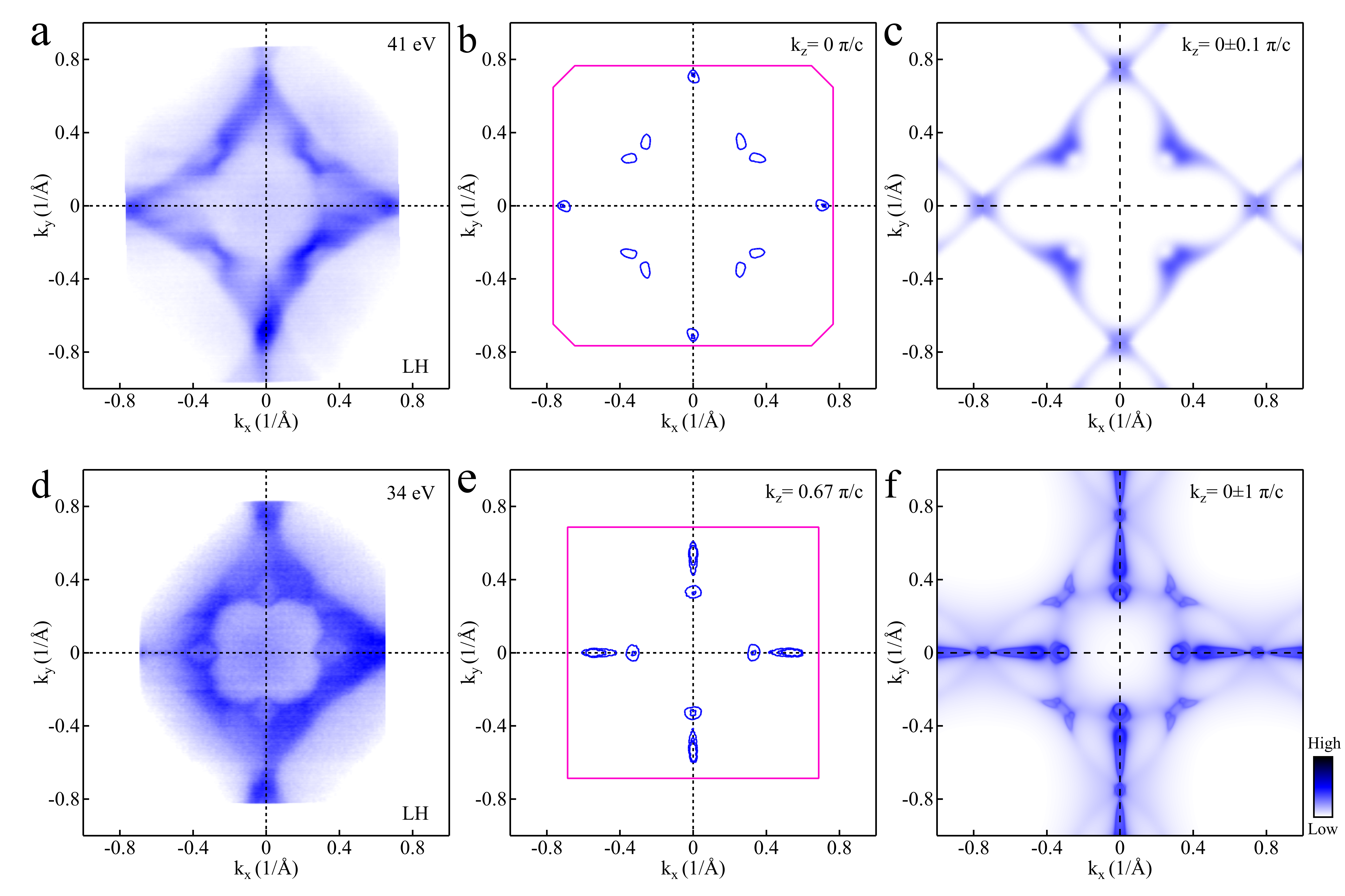
So far, we can confirm that the electronic structure measured in area 1 (the flat area) is mainly from the surface states and the electronic structures measured in area 2 (the area with multiple steps) is mainly from the bulk states. According to the previous report, bulk state measurements with photon energy of 41 eV corresponds to the k 0 plane and a photon energy of 34 eV corresponds to the k 0.67 plane[15]. Therefore, Fermi surface measurements with photon energies of 41 eV (Fig. 3a) and 34 eV (Fig. 3d) were done in area 2 and compared to the DFT calculated bulk Fermi surfaces at the k 0 (Fig. 3b) and the k 0.67 (Fig. 3e) planes. We note that the measured Fermi surfaces (Fig. 3a and 3d) appear to have more features than the calculated Fermi surfaces (Fig. 3b and 3e). This is especially so for the Fermi surface measured with 34 eV photon energy (Fig. 3d), which has a rhomboid like shape with four arc like features in addition to the Fermi surface features in Fig. 2e. The rhomboid and four-arcs-like Fermi surface can also be observed in Fig. 3a. Some extra band features are similarly observed in the band dispersion measurements shown in Fig. S1 in the Supplemental Material. Recently a report on the complete suppression of trivial surface states on NbP was published[13]. By preparing a dangling bond free P terminated surface, the trivial surface states of NbP were fully suppressed, resulting in a purely topological Fermi arc dispersion on the surface. While this could indicate that the observed rhomboid and four-arcs-like Fermi surface in Fig. 3a and 3d are potential topological surface states, further analysis reveals that they are not (see the Supplemental Material for details). To further clarify the origin of these states, we performed DFT calculations of the bulk Fermi surface at kz= 0 plane taking into account a kz resolution of 0.2 and 2 , as shown in Fig. 3c and 3f. The DFT calculations of the bulk Fermi surface at kz= 0.67 plane with a kz resolution of 0.2 is included in the Supplemental Material. Comparing the measured Fermi surface features taken with photon energy of 41 eV in Fig. 3a to the DFT calculated Fermi surface at kz= 0 plane with a kz resolution of 0.2 (Fig. 3c), we find that the two agree well. However, the DFT calculated Fermi surface at kz= 0.67 considering a kz resolution of 0.2 (see the Supplemental Material for details) is not completely consistent with the Fermi surface measured at 34 eV. On the other hand, integrating along kz across the complete BZ, the DFT calculated Fermi surface captures all the features of the Fermi surface (Fig. 3d) measured with 34 eV photons. This can be a sign of stronger final state effects and vanishing resolution at a photon energy of 34 eV. These results points to both the trivial and topological surface states being fully suppressed on NdAlSi for the uneven sample surfaces.
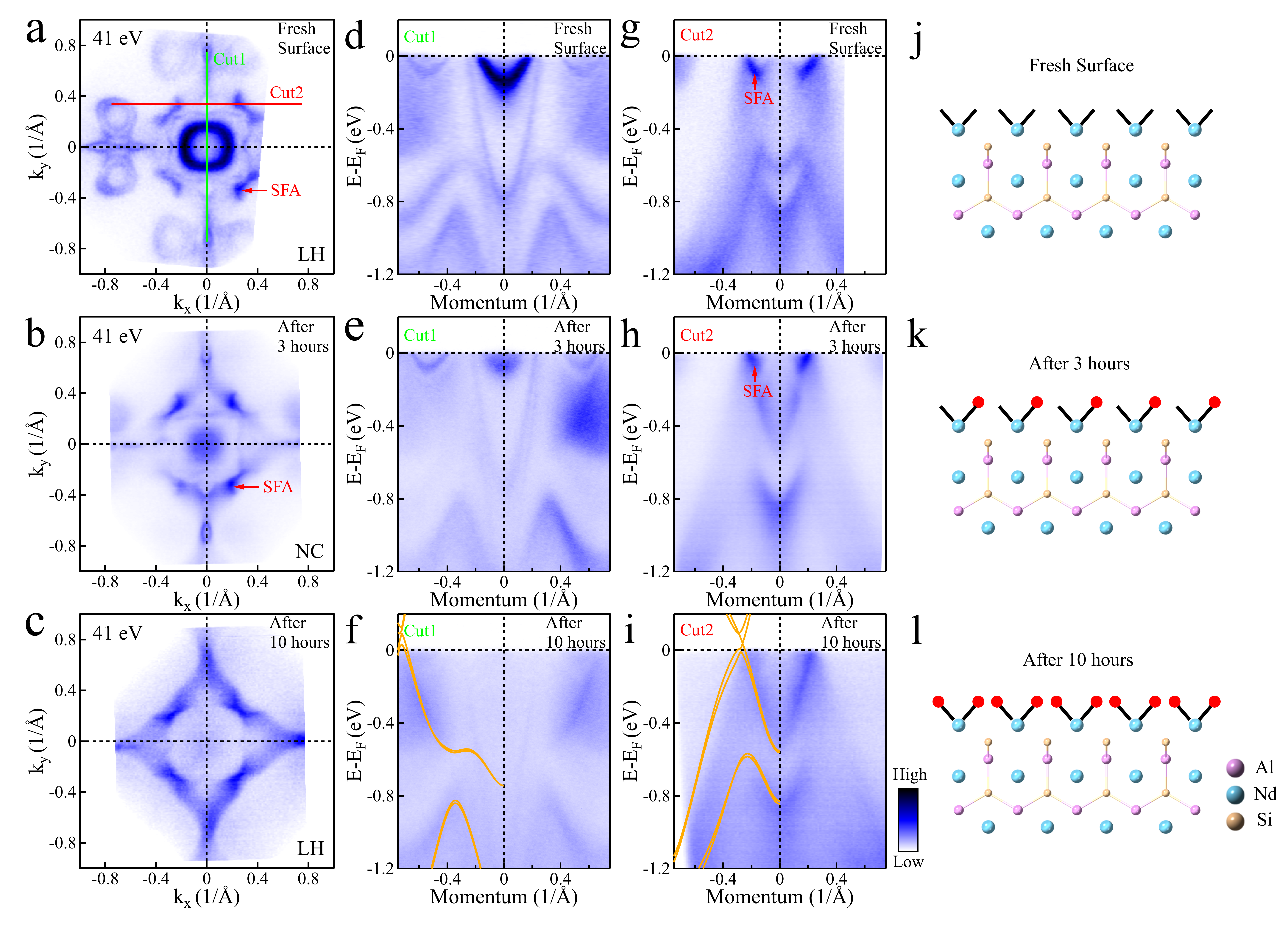
In order to clarify the reason for this effect, we carried out time dependent electronic structure measurements in the flat areas (area 1 in Fig. 2a) of the sample. In this case, all of the surface states (trivial surface states and SFAs) can be clearly observed when measured in area 1 of the newly cleaved sample, as shown in Fig. 4a, 4d and 4g. However, three hours later, the surface state appears blurred (Fig. 4b, 4e and 4h) relative to the newly cleaved sample, and some structures of the surface state (the electron like band in the center of the BZ, Fig. 4e) even shift to higher energy. Ten hours later, all of the surface states (trivial surface states and SFAs) seem to be completely suppressed and only bulk states appear, as shown in Fig. 4c, 4f and 4i. This is similar to the electronic structures measured in area 2 of the newly cleaved sample (Fig. 2f and 2g). At this point, we conjecture an explanation for the suppression of surface states on the uneven sample surface of NdAlSi. Since there are many unsatisfied dangling bonds on the surface of the freshly cleaved sample, as shown in Fig. 4j. These unsatisfied dangling bonds create localized electronic states within the band gap of the material. The localized electronic states are the trivial surface states that we observe. The uneven sample surface should show stronger adsorption than the flat sample surface and thus increased adsorb of impurities. Therefore, after sample cleavage, the uneven sample surface adsorbs enough impurities in a short time to saturate the dangling bonds on the surface, thus destroying the trivial surface states. While for flat surfaces, it takes longer to adsorb enough impurities to saturate the dangling bonds on the surface, as shown in the schematic diagram Fig. 4k-4l. At the same time, we also notice that in the time dependent electronic structure measurements, ten hours post sample cleavage, the original clear SFAs (Fig. 4g) also disappears but the bulk electronic structure can be clearly observed when measured on the flat surface (Fig. 4i). Since the topological surface states in Weyl semimetal are not directly related to dangling bonds, which arise from the non-trivial topology of the bulk electronic structure, we do not expect these states to disappear. A potential explanation for this behavior is that the adsorption results in surface disorder which in turn disrupts the topological surface states and pushes them down to the underlying ordered layer. This conjecture is supported by recent STM measurements[16]. After sample cleavage, the Nd terminated surface forms a metallic bond with the underlying Si atomic layer, which is very soft and easily form clusters that result in a disordered surface[16]. Interestingly, however, the saturation of the dangling bonds and the formation of atomic clusters on the surface, which completely suppress the surface states do not result in any observable shift of the bulk state Fermi energy.
In summary, by carrying out ARPES measurements on the Weyl semimetal NdAlSi, we found that all of the surface states, trivial surface states as well as SFAs, were suppressed on uneven surfaces while there is no noticeable Fermi energy shift in the bulk states. The observed temporal evolution of the electronic structure further suggests that the suppression of trivial surface states on uneven surfaces may be linked to the more accessible saturation of dangling bonds associated with these trivial surface states. Our findings demonstrate an approach to directly measure the intrinsic bulk states using low photon energies in ARPES and provides insights into ways of effectively manipulating surface states in topological materials.
Methods
Sample Single crystals of NdAlSi were grown from Al as flux. Nd, Al, Si elements were sealed in an alumina crucible with the molar ratio of 1: 10: 1. The crucible was finally sealed in a highly evacuated quartz tube. The tube was heated up to 1273 K, maintained for 12 hours and then cooled down to 973 K at a rate of 3 K per hour. Single crystals were separated from the flux by centrifuging. The Al flux attached to the single crystals were removed by dilute NaOH solution.
ARPES Measurements High-resolution ARPES measurements were performed at the I05 beamline of the Diamond synchrotron. The total energy resolution (analyzer and beamline) was set at 1520 meV for the measurements. The angular resolution of the analyser was 0.1 degree. The beamline spot size on the sample was about 70 m70 m at the I05 beamline of the Diamond synchrotron. The samples were cleaved in situ and measured at about 10 K in ultrahigh vacuum with a base pressure better than 1.010-10 mbar.
DFT calculations The electronic structure calculations for NdAlSi were performed based on the density functional theory (DFT)[17, 18] as implemented in the VASP package[19, 20]. The generalized gradient approximation (GGA) of Perdew-Burke-Ernzerhof (PBE) type[21] was chosen for the exchange-correlation functional. The projector augmented wave (PAW) method[22, 23] was adopted to describe the interactions between valence electrons and nuclei. In the calculation of the paramagnetic phase of NdAlSi, the Nd pseudopotential was chosen without the 4 electrons. The kinetic energy cutoff of the plane-wave basis was set to be 350 eV. A 161616 Monkhorst-Pack grids[24] was used for the BZ sampling. For describing the Fermi-Dirac distribution function, a Gaussian smearing of 0.05 eV was used. For structure optimization, both lattice parameters and internal atomic positions were fully relaxed until the forces on all atoms were smaller than 0.01 eV/Å. The relaxed lattice constants are: = 4.22 Å and = 14.59 Å, which agree well with the experimental measurements[25]. The spin-orbit coupling effect was also included for studying the non-trivial band topology. For further studying the surface states of NdAlSi, we employed a 36 atomic layers slab system with 20 Å vacuum separation. The orbital weights of the top three atomic layers were calculated as the surface states with respect to the corresponding terminal surfaces.
Data Availability
The authors declare that all data supporting the findings of this study are available within the paper and its Supplementary Information files.
References
- [1] I. Tamm, Ueber eine moegliche Art der Elektronenbindung an Kristalloberflaechen. Z. Phys. 76, 849 (1932).
- [2] W. Shockley, On the surface states associated with a periodic potential. Phys. Rev. 56, 317 (1939).
- [3] M. Z. Hasan and C. L. Kane, Colloquium: topological insulators. Rev. Mod. Phys. 82, 3045 (2010).
- [4] X. L. Qi and S. C. Zhang, Topological insulators and superconductors. Rev. Mod. Phys. 83, 1057 (2011).
- [5] K. Manna et al., Heusler, Weyl and Berry. Nat. Rev. Mater. 3 244 (2018).
- [6] N. P. Armitage et al., Weyl and Dirac semimetals in three-dimensional solids. Rev. Mod. Phys. 90, 015001 (2018).
- [7] B. Q. Lv et al., Experimental perspective on three-dimensional topological semimetals. Rev. Mod. Phys. bf 93, 025002 (2021).
- [8] R. Karplus et al., Hall effect in ferromagnetics. Phys. Rev. 95, 1154 (1954).
- [9] F. D. M. Haldane et al., Berry Curvature on the Fermi Surface: Anomalous Hall Effect as a Topological Fermi-Liquid Property. Phys. Rev. Lett. 93, 206602 (2004).
- [10] Y. Machida et al., Time-reversal symmetry breaking and spontaneous Hall effect without magnetic dipole order. Nature 463, 210 (2010).
- [11] S. Murakami et al., Dissipationless Quantum Spin Current at Room Temperature. Science 301, 1348 (2003).
- [12] J. Sinova et al., Universal intrinsic spin Hall effect. Phys. Rev. Lett. 92, 126603 (2004).
- [13] A. B. Pinto et al., Large Fermi-Energy Shift and Suppression of Trivial Surface States in NbP Weyl Semimetal Thin Films. Adv. Mater. 33, 2008634 (2021).
- [14] J. Gaudet et al., Weyl-mediated helical magnetism in NdAlSi. Nat. Mater. 20, 1650 (2021).
- [15] C. Li et al., Emergence of Weyl fermions by ferrimagnetism in a noncentrosymmetric magnetic Weyl semimetal. Nat. Commun. 14, 7185 (2023).
- [16] C. Li et al., Bulk Boundary Paradox in the Surface Reconstructed Magnetic Weyl Semimetal NdAlSi. arXiv:
- [17] P. Hohenberg and W. Kohn, Inhomogeneous Electron Gas. Phys. Rev. 136, B864 (1964).
- [18] W. Kohn and L. J. Sham, Self-Consistent Equations Including Exchange and Correlation Effects. Phys. Rev. 140, A1133 (1965).
- [19] G. Kresse and J. Furthmller, Efficiency of ab-initio total energy calculations for metals and semiconductors using a plane-wave basis set. Comput. Mater. Sci. 6, 15 (1996).
- [20] G. Kresse and J. Furthmller, Efficient iterative schemes for ab initio total-energy calculations using a plane-wave basis set. Phys. Rev. B 54, 11169 (1996).
- [21] J. P. Perdew et al., Generalized Gradient Approximation Made Simple. Phys. Rev. Lett. 77, 3865 (1996).
- [22] P. E. Blöchl, Projector augmented-wave method. Phys. Rev. B 50, 17953 (1994).
- [23] G. Kresse and D. Joubert, From ultrasoft pseudopotentials to the projector augmented-wave method. Phys. Rev. B 59, 1758 (1998).
- [24] H. J. Monkhorst and J. D. Pack, Special points for Brillonin-zone integrations. Phys. Rev. B 13, 5188 (1976).
- [25] J. F. Wang et al., NdAlSi: A magnetic Weyl semimetal candidate with rich magnetic phases and atypical transport properties. Phys. Rev. B 105, 144435 (2022).
Acknowledgement
The work presented here was financially supported by the Swedish Research council (2019-00701) and the Knut and Alice Wallenberg foundation (2018.0104). Y.G.S. acknowledges the National Natural Science Foundation of China (Grants No. U2032204), and the Informatization Plan of Chinese Academy of Sciences (CAS-WX2021SF-0102).
Author Contributions
C.L. proposed and conceived the project. C.L. carried out the ARPES experiments with the assistance from W.Y.C.. J.F.Z. and T.X. contributed to the band structure calculations and theoretical discussion. H.X.L. and Y.G.S. contributed to NdAlSi crystal growth. C.L. contributed to software development for data analysis and analyzed the data. C.L. wrote the paper. T.K. provided the beamline support. O.T. contributed to the scientific discussions and revision of the manuscript. All authors participated in and commented on the paper.
Competing Interests
The authors declare no competing interests.


