Low frequency resistance fluctuations in an ionic liquid gated channel probed by cross-correlation noise spectroscopy
Abstract
A system in equilibrium keeps “exploring” nearby states in the phase space and consequently, fluctuations can contain information, that the mean value does not. However, such measurements involve a fairly complex interplay of effects arising in the device and measurement electronics, that are non-trivial to disentangle. In this paper, we briefly analyse some of these issues and show the relevance of a two-amplifier cross-correlation technique for semiconductors and thin films commonly encountered. We show that by using home-built amplifiers costing less than 10 USD/piece one can measure spectral densities as low as . We apply this method to an ionic liquid gated Ga:ZnO channel and show that the glass transition of the ionic liquid brings about a change in the exponent of the low frequency resistance fluctuations. Our analysis suggests that a log-normal distribution of the Debye relaxation times of the fluctuations and an increased weight of the long timescale relaxations can give a semi-quantitative explanation of the observed change in the exponent.
A key problem encountered in all measurements of “noise” is that the recorded data always contains the noise originating from the sample/DUT (Device under test) and the measurement circuit, in particular the first stage amplifier. There are two generic approaches to this aspect.
-
1.
One ensures that the first stage amplifier’s noise is assuredly less than the DUT. In literature [1] it is often addressed by choosing a passive small-signal transformer (PST) as the first stage. These transformers with very high core susceptibility [2, 3] often have noise contribution as low as and certain more specialised designs can even be operated at cryogenic temperatures. While these give excellent Common-mode-rejection (CMRR), the limitation is that the input impedances these can handle are limited (typically ). It is important to point out that the impedance seen by the amplifier is always the “2-terminal” resistance which includes the typical lead-resistance of a cryostat (or similar equipment) and ohmic-contact resistance of the DUT itself. Even in cases where the 4-terminal resistance of the DUT is very small the resistance seen by the transformer is not necessarily small due to these inevitable contributions appearing in series. Another aspect is that since no transformer can be truly d.c. coupled, the very low frequency resistance fluctuations can only be measured by modulating them with a relatively higher frequency current, effectively translating the resulting voltage fluctuations to the most sensitive area of the transformer’s own noise figure.
-
2.
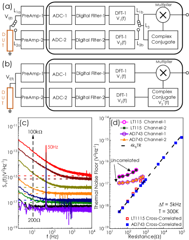
Another approach is to use reasonably low noise but d.c. coupled and relatively inexpensive (in our experiments, the chips used are all priced below 10 USD) BJT/FET input operational amplifiers, that can handle significantly higher input impedances but will have an intrinsic input noise typically a factor of higher compared to the PST. The resistances encountered in measurements on semiconductors [4, 5, 6, 7, 8], carbon nanotube [9, 10], Indium arsenide nanowires [11, 12] and 2D materials [13, 14, 15, 16, 17, 18, 19, 20, 21, 22] are often in the range of - . In this method, the voltage signal is fed in parallel to two nearly identical first-stage amplifiers powered from independent and uncorrelated sources. Their outputs are then simultaneously digitised (in our experiments with bit resolution in range and at a rate of up to ), discrete Fourier transformed (DFT) after passing through an anti-aliasing filter and then cross-correlated in the frequency domain. In certain niche applications, like detecting shot noise [23, 24] or thermal noise [25, 26] in mesoscopic conductors for probing quantum statistics [24, 27, 28], the granularity of charge [29] etc., the signals are handled through similar techniques of auto or cross-correlation. This is achieved by employing an initial-stage cryogenic amplifier (at K) with a typical gain of [30] combined with a room-temperature one. They are often designed to operate at a few MHz. This approach ensures the primary amplification of the signal in close proximity to the sample, preventing the accumulation of undesired signals before being seen by the room temperature electronics. As described [31, 32] the cross-correlation process largely (but not entirely) eliminates the uncorrelated noise from the amplifiers themselves. The resulting output is the spectral density of the signal that was “common” to both the amplifiers. While this suffices for a large class of experiments with Gaussian fluctuations, it should be borne in mind that the original time series cannot be reconstructed.
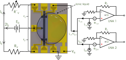
Our implementation of the cross correlation technique is shown in Fig. 1. The sample itself forms two arms, assumed to have resistances and , of a Wheatstone bridge with much larger resistances and forming two other arms. One of the large resistances is adjustable and is used to null the bridge output. We have and . The output is then largely immune to small fluctuations of the biasing source () and the ambient temperature, as fluctuations arising out of these will tend to affect and almost identically. However, a small resistance fluctuation in one of the arms (due to internal processes like trapping-de-trapping, thermal generation etc.) will be picked up. This signal is then fed to both the amplifiers (each of gain ), as shown and their outputs cross-correlated. The expected (cross-correlated) power spectral density of the voltage fluctuations arising from these resistance fluctuations, when current flows through the DUT is given by Eq. (1)[1],
| (1) |
where is the power spectrum of the background originating from electronic and thermal noise, is the spectrum of with long time average . The choice of the first-stage amplifier is guided by a balance between the inevitable intrinsic input current and the current noise of the operational amplifier itself. Fig. 1 shows the equivalent circuit with the noise equivalent sources included as part of the input stages. It is not only the DUT voltage but the combination (see Fig. 1) of three voltages that would get amplified. They are related as follows :
| (2) |
Ultimately this determines the practicality of the measurement. We find that a current noise not exceeding few and a voltage noise not exceeding are essential for most measurements. Choosing an amplifier with lower voltage noise but higher current noise is detrimental once the resistance of the DUT becomes slightly higher, in which case the noise current flowing through the DUT manifests itself as a much higher voltage noise over-ruling the benefit of a lower voltage noise. Although, for very low source resistances, this would be acceptable. However, our purpose is to design an inexpensive and generic setup covering the typical range of resistances encountered in semiconductors and similar samples whose resistances may well go up to several tens of . This is illustrated with two commonly available operational amplifiers in Fig. 2(d). If no cross-correlation is used, the spectrum obtained corresponds to the two upper curves (Uncorrelated). However, once the two data are cross-correlated the contribution from the amplifiers is suppressed to a large extent and the correct thermal noise (with no adjustable parameters) is obtained over more than four orders of magnitude, spanning - .
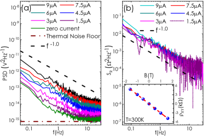
The typical behaviour of has a well defined nearly flat high frequency () part and a low frequency () , with (Fig. 2(c)). The correctness of the absolute values produced by the cross-correlation technique can be judged by two observations.
- 1.
-
2.
The correctness of the low-frequency part can be established by ascertaining the magnitude of the Hooge parameter [35, 36] given by
(3) Notice that this requires knowing the total number of carriers () participating in the conduction process. We used a well-characterised 2D electron gas (2DEG) in a GaAs-AlGaAs High electron mobility transistor (HEMT) below the surface and hence mostly free from the effect of scattering from the charged surface states and oxide monolayers. Hall measurements on the HEMT yielded a carrier density of and a room temperature mobility of The dimensions of the etched mesa was and the resistance between the pair of contacts used was at . Using the data of Fig. 3(b) and the above-mentioned numbers we get , which is very close to the values reported by Hooge [36, 35] when the origin of the noise is primarily in the bulk.
The presence of a parallel layer of charge at some distance from a 2D electron or hole gas (2DEG/2DHG) is a common feature in heterostructures. Either the modulation doped layer, a delta doped layer or the charged surface states (in the case of a shallow 2DEG) create an impurity potential in the plane of the 2D system. This potential, screened by the 2DEG and suitably averaged over its form factor is one of the major sources of scattering that limits the transport [37, 38, 39, 40] as well as the quantum lifetime [41, 42]. While for relatively lower carrier density systems like MOSFETs, GaAs-AlGAs HEMT and HHMTs (High hole mobility transistors) a dielectric-metal gate is used to modulate the carrier densities, the technique becomes untenable when the carrier densities are very high. In several systems of recent interest [43, 44, 45, 46, 47, 48] modulation of carrier densities is possible only via ionic liquid (IL) gates capable of forming self-organized nano gap capacitors upon application of gate voltage, resulting in capacitance in the range of [49, 50, 43, 45, 51, 46, 52]. For the IL gated system, the electric double layer is effectively a very high density surface charge. However, systems gated with IL are also inherently very high carrier density systems and the impurity Coulomb potential would be screened. Thomas-Fermi screening gives where the Thomas-Fermi wave vector is given by . The density of states at the Fermi level makes sufficiently large to suppress large angle scattering which has a maximal effect on transport lifetime (i.e. mobility ). However, it is known that as the IL nears the glass transition temperature from the high temperature side, the short time fluctuations are gradually frozen out irrespective of the gate voltage. It is seen experimentally that most of the time the resistivity of the conducting channel itself does not have any sharp feature as the IL crosses (for DEME-TFSI used in our experiments ). However, our investigations show that the exponent of the low frequency resistance noise ( , using the method described earlier) in an IL gated has a pronounced change. The results are valid over three to four decades of frequency. While transport and photo-response using an ionic liquid () gate has been reported n-ZnO samples [53, 54], the temperature dependence of low frequency noise in these IL-FET has not been previously explored.
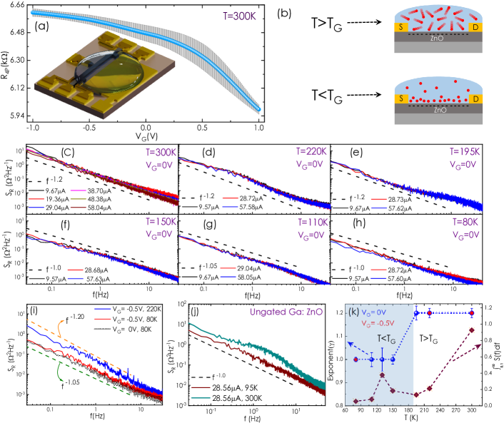
Our sample (Fig. 4(a)) is a Ga-doped ZnO thin film deposited on c-sapphire by RF magnetron reactive co-sputtering of Zn and at 375°C with 3% of coverage on the Zn target, in sputtering atmosphere. Subsequently, these are lithographically patterned into Hall bars with 100 and =1150 and contact pads. Hall measurement (Supplementary data) gives a carrier density of . The four-terminal resistivity is . This yields a Hall mobility , at . While applying on the channel, the contacts were covered with silicone gel to protect them [55]. After application, it was cured in a high vacuum at for 48 hrs. By making the gate electrode much larger than the channel area, the necessity of a reference electrode was eliminated since most of the potential will drop across the working electrode [52]. At room temperature, the gate voltage sweep shows a near variation of the resistance for applied of , shown in Fig. 4(a).
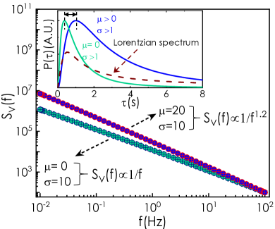
The measurement of noise was carried out from to well below , as shown in Fig. 4(c)-(j). We find that for the exponent with no strong dependence on the gate voltage. For , it is clear that , as summarised in Fig. 4(k). The magnitude of the noise has a small peak around the transition region. The noise at low frequencies is thought to arise from fluctuations with Debye-type relaxation having distributions of the relaxation time over several decades of frequencies. The distribution of the relaxation times indeed affects the power law [35]. We show that by assuming a physically reasonable log-normal distribution whose mean () is slightly shifted but the spread () is essentially kept constant, we can reproduce in a simple parametric way, variations of the exponent of the low frequency fluctuations. This can be expressed as,
| (4) |
where, is the log normal distribution function. Fig. 5 shows the results of the numerically computed integral from Eq. (4) with the mean of the distribution shifted slightly towards the higher values of (as shown in the inset). The physical interpretation of this is that the weightage of the faster fluctuations, i.e. smaller values of are slightly reduced. This is consistent with the expectation that as the temperature is reduced below the glass transition temperature some of the relatively faster fluctuations are essentially frozen, affecting the distribution over which the Lorentzian relaxations must be summed over.
In conclusion, we have presented a relatively inexpensive method of measuring low frequency noise that largely eliminates the noise originating in the measurement electronics. The method is also suited for a very wide range of input impedances that are encountered in many systems of current interest. We applied this method to an IL-gated degenerate semiconductor and showed that the exponent of the noise changes as the ionic liquid undergoes the glass transition. We linked this to a physically reasonable distribution of the relaxation times. While we have not tried to do a microscopic first principle derivation of this distribution, we note that it is a reasonable and simply parametrizable distribution that appears to correctly reproduce the nature of variation of the exponent of the
noise observed in our system as well as several others. The distribution can be further tuned in two significant ways that may be of physical importance. First, the spread of the distribution itself may be related to certain aspects of the interfacial defects. In addition, if there are specific recombination-generation processes occurring with a certain time scale [56] an additional weight at that time scale can be added to the smooth background to reproduce the humps that are sometimes observed in this type of measurement.
Acknowledgements: BCB and AKJ acknowledge financial support through DST-INSPIRE and UGC fellowships of Govt. of India. Low temperature measurements were supported by the cryogenic facilities of IIT Bombay. We thank S.K. Appani and S.S. Major (Dept of Physics, IIT Bombay) for providing the Ga:ZnO samples.
References
- Scofield [1987] J. H. Scofield, Review of scientific instruments 58, 985 (1987).
- [2] Stanford Research Systems, Model SR554 Transformer Pre-amplifier (Stanford Research Systems, 1290-D Reamwood Ave. Sunnyvale, CA 94089).
- Signal Recovery Systems () [Ametek] Signal Recovery Systems (Ametek), Model 1900 Transformer Input Preamplifier ( Ametek Scientific Instruments, Berwyn, Pennsylvania, U.S.).
- Peransin et al. [1990] J.-M. Peransin, P. Vignaud, D. Rigaud, and L. K. Vandamme, IEEE transactions on electron devices 37, 2250 (1990).
- Lee [2009] P. Lee, Analog Devices Application Note, AN-940 (2009).
- Shao et al. [2009] Q. Shao, G. Liu, D. Teweldebrhan, A. A. Balandin, S. Rumyantsev, M. S. Shur, and D. Yan, IEEE Electron Device Letters 30, 288 (2009).
- Watanabe et al. [2018] S. Watanabe, H. Sugawara, R. Häusermann, B. Blülle, A. Yamamura, T. Okamoto, and J. Takeya, Communications Physics 1, 37 (2018).
- Ma et al. [2019] X. Ma, J. Zhang, W. Cai, J. Wilson, and A. Song, ACS Applied Electronic Materials 1, 972 (2019).
- Collins et al. [2000] P. G. Collins, M. Fuhrer, and A. Zettl, Applied Physics Letters 76, 894 (2000).
- Appenzeller et al. [2007] J. Appenzeller, Y.-M. Lin, J. Knoch, Z. Chen, and P. Avouris, IEEE transactions on nanotechnology 6, 368 (2007).
- Delker et al. [2012] C. J. Delker, S. Kim, M. Borg, L.-E. Wernersson, and D. B. Janes, IEEE transactions on electron devices 59, 1980 (2012).
- Delker et al. [2013] C. J. Delker, Y. Zi, C. Yang, and D. B. Janes, IEEE transactions on electron devices 60, 2900 (2013).
- Mehra et al. [2023] A. Mehra, R. J. Mathew, and C. Kumar, Applied Physics Letters 123 (2023).
- Pal and Ghosh [2009a] A. N. Pal and A. Ghosh, Applied Physics Letters 95 (2009a).
- Pal et al. [2011] A. N. Pal, S. Ghatak, V. Kochat, E. Sneha, A. Sampathkumar, S. Raghavan, and A. Ghosh, ACS nano 5, 2075 (2011).
- Pal and Ghosh [2009b] A. N. Pal and A. Ghosh, Physical Review Letters 102, 126805 (2009b).
- Kamada et al. [2023] M. Kamada, W. Zeng, A. Laitinen, J. Sarkar, S.-S. Yeh, K. Tappura, H. Seppä, and P. Hakonen, Communications Physics 6, 207 (2023).
- Karnatak et al. [2016] P. Karnatak, T. P. Sai, S. Goswami, S. Ghatak, S. Kaushal, and A. Ghosh, Nature communications 7, 13703 (2016).
- Kamada et al. [2021] M. Kamada, A. Laitinen, W. Zeng, M. Will, J. Sarkar, K. Tappura, H. Seppa, and P. Hakonen, Nano Letters 21, 7637 (2021).
- Pal et al. [2010] A. N. Pal, A. A. Bol, and A. Ghosh, Applied Physics Letters 97 (2010).
- Heller et al. [2010] I. Heller, S. Chatoor, J. Männik, M. A. G. Zevenbergen, J. B. Oostinga, A. F. Morpurgo, C. Dekker, and S. G. Lemay, Nano Letters 10, 1563 (2010).
- Moulick et al. [2022] S. Moulick, R. Alam, and A. N. Pal, ACS Applied Materials & Interfaces 14, 51105 (2022).
- Oliver et al. [1999] W. D. Oliver, J. Kim, R. C. Liu, and Y. Yamamoto, Science 284, 299 (1999).
- Kapfer et al. [2019] M. Kapfer, P. Roulleau, M. Santin, I. Farrer, D. Ritchie, and D. Glattli, Science 363, 846 (2019).
- Dutta et al. [2022] B. Dutta, V. Umansky, M. Banerjee, and M. Heiblum, Science 377, 1198 (2022).
- Le Breton et al. [2022] G. Le Breton, R. Delagrange, Y. Hong, M. Garg, K. Watanabe, T. Taniguchi, R. Ribeiro-Palau, P. Roulleau, P. Roche, and F. Parmentier, Physical Review Letters 129, 116803 (2022).
- Bartolomei et al. [2020] H. Bartolomei, M. Kumar, R. Bisognin, A. Marguerite, J.-M. Berroir, E. Bocquillon, B. Placais, A. Cavanna, Q. Dong, U. Gennser, et al., Science 368, 173 (2020).
- Glidic et al. [2023] P. Glidic, O. Maillet, A. Aassime, C. Piquard, A. Cavanna, U. Gennser, Y. Jin, A. Anthore, and F. Pierre, Physical Review X 13, 011030 (2023).
- Assouline et al. [2023] A. Assouline, L. Pugliese, H. Chakraborti, S. Lee, L. Bernabeu, M. Jo, K. Watanabe, T. Taniguchi, D. Glattli, N. Kumada, et al., Science 382, 1260 (2023).
- DiCarlo et al. [2006] L. DiCarlo, Y. Zhang, D. McClure, C. Marcus, L. Pfeiffer, and K. West, Review of Scientific Instruments 77 (2006).
- Jain et al. [2018] A. K. Jain, H. Nigudkar, H. Chakraborti, A. Udupa, and K. D. Gupta, in AIP Conference Proceedings, Vol. 1942 (AIP Publishing, 2018) p. 060020.
- [32] B. C. Barik, H. Chakraborti, A. Jain, B. Pal, and K. Das Gupta, Supplementary data .
- Nyquist [1928] H. Nyquist, Physical review 32, 110 (1928).
- Reif [1998] F. Reif, Fundamentals of statistical and thermal physics (1998).
- Hooge et al. [1981] F. Hooge, T. Kleinpenning, and L. Vandamme, Reports on progress in Physics 44, 479 (1981).
- Dutta and Horn [1981] P. Dutta and P. Horn, Reviews of Modern physics 53, 497 (1981).
- Ando et al. [1982] T. Ando, A. B. Fowler, and F. Stern, Rev. Mod. Phys. 54, 437 (1982).
- Davies [1998] J. H. Davies, The Physics of Low Dimensional Semiconductors (Cambridge University Press, 1998).
- Mak et al. [2010] W. Y. Mak, K. Das Gupta, H. E. Beere, I. Farrer, F. Sfigakis, and D. A. Ritchie, Applied Physics Letters 97, 242107 (2010).
- Kozlov et al. [2007] D. A. Kozlov, Z. D. Kvon, A. K. Kalagin, and A. I. Toropov, Semiconductors 31, 242107 (2007).
- Wang et al. [2013] D. Q. Wang, J. C. H. Chen, O. Klochan, K. Das Gupta, D. Reuter, A. D. Wieck, D. A. Ritchie, and A. R. Hamilton, Phys. Rev. B 87, 195313 (2013).
- Hong et al. [2009] X. Hong, K. Zou, and J. Zhu, Physical Review B 80, 241415 (2009).
- Daghero et al. [2012] D. Daghero, F. Paolucci, A. Sola, M. Tortello, G. Ummarino, M. Agosto, R. Gonnelli, J. R. Nair, and C. Gerbaldi, Physical review letters 108, 066807 (2012).
- Sagmeister et al. [2006] M. Sagmeister, U. Brossmann, S. Landgraf, and R. Würschum, Physical review letters 96, 156601 (2006).
- Petach et al. [2014] T. A. Petach, M. Lee, R. C. Davis, A. Mehta, and D. Goldhaber-Gordon, Physical Review B 90, 081108 (2014).
- Piatti et al. [2017] E. Piatti, D. Daghero, G. Ummarino, F. Laviano, J. Nair, R. Cristiano, A. Casaburi, C. Portesi, A. Sola, and R. Gonnelli, Physical Review B 95, 140501 (2017).
- Piatti et al. [2022] E. Piatti, M. Colangelo, M. Bartoli, O. Medeiros, R. S. Gonnelli, K. K. Berggren, and D. Daghero, Physical Review Applied 18, 054023 (2022).
- Yuan et al. [2009] H. Yuan, H. Shimotani, A. Tsukazaki, A. Ohtomo, M. Kawasaki, and Y. Iwasa, Advanced Functional Materials 19, 1046 (2009).
- Lu et al. [2015] J. Lu, O. Zheliuk, I. Leermakers, N. F. Yuan, U. Zeitler, K. T. Law, and J. Ye, Science 350, 1353 (2015).
- Costanzo et al. [2016] D. Costanzo, S. Jo, H. Berger, and A. F. Morpurgo, Nature nanotechnology 11, 339 (2016).
- Ueno et al. [2011] K. Ueno, S. Nakamura, H. Shimotani, H. Yuan, N. Kimura, T. Nojima, H. Aoki, Y. Iwasa, and M. Kawasaki, Nature nanotechnology 6, 408 (2011).
- Yuan et al. [2010] H. Yuan, H. Shimotani, J. Ye, S. Yoon, H. Aliah, A. Tsukazaki, M. Kawasaki, and Y. Iwasa, Journal of the American Chemical Society 132, 18402 (2010).
- Ghimire et al. [2015] R. R. Ghimire, S. Mondal, and A. Raychaudhuri, Journal of Applied Physics 117 (2015).
- Mondal et al. [2015] S. Mondal, R. R. Ghimire, and A. Raychaudhuri, Applied Physics Letters 106 (2015).
- Misra et al. [2007] R. Misra, M. McCarthy, and A. F. Hebard, Applied Physics Letters 90, 052905 (2007).
- Ghosh et al. [2024] S. Ghosh, Z. E. Nataj, F. Kargar, and A. A. Balandin, arXiv preprint arXiv:2401.12432 (2024).
See pages - of SM.pdf