Cross talk of a large-scale depleted monolithic active pixel sensor (DMAPS) in \qty180\nano CMOS technology
Abstract
Monolithic pixel detectors combine readout electronics and sensor in a single entity of silicon, which simplifies the production procedure and lowers the material budget compared to conventional hybrid pixel detector concepts. Benefiting from the advances in commercial CMOS processes towards large biasing voltage capabilities and the increasing availability of high-resistivity substrates, depleted monolithic active pixel sensors (DMAPS) are able to cope with the high-rate and high-radiation environments faced in modern high-energy physics experiments. TJ-Monopix2 is the latest iteration of a DMAPS development line designed in \qty180\nano TowerSemicondutor technology, which features a large scale \qtyproduct2x2\centi chip divided into \qtyproduct512x512pixels with a pitch of \qtyproduct33x33\micro. All in-pixel electronics are separated from its small collection electrode and process modifications are implemented to improve charge collection efficiency especially after irradiation. The latest laboratory measurements and investigations of a threshold variation observed for TJ-Monopix2 in typical operating conditions are presented.
keywords:
Pixel detector, Monolithic pixel, CMOS sensor, DMAPS[1]organization=Physikalisches Institut der Universität Bonn, addressline=Nußallee 12, city=Bonn, country=Germany
[5]organization=CERN, addressline=Espl. des Particules 1, city=Meyrin, country=Switzerland
1 Introduction
The recent advancements in commercial CMOS technologies propel the development of monolithic active pixel sensors (MAPS), which combine readout electronics and sensor in a single piece of silicon [1]. This design approach simplifies the production procedure and reduces the material budget compared to the hybrid pixel detector concept. Additional use of high-resistivity bulk substrates () combined with sufficiently large bias voltage capabilities facilitate the depletion of the sensitive volume and improve the fast charge collection by drift across a pixel [2, 3]. Hence, depleted MAPS (DMAPS) have an increased radiation tolerance making them a promising candidate for high-rate and high-radiation environment applications as faced in modern high-energy particle physics experiments. By implementing a small collection electrode relative to the pixel pitch, the in-pixel electronics need to be separated and are placed in distinct p-wells. This design approach yields a reduction in sensor capacitance, thereby facilitating both low power consumption and enhanced threshold performance. The long drift distances to the small collection node render the sensor more prone to radiation damage that require additional process modifications in the sensor layout. The latest prototype of the TJ-Monopix DMAPS development line, TJ-Monopix2, is a large-scale chip designed in \qty180\nano CMOS technology and high-resistivity substrate for compliance with the outer layer requirements of the ATLAS Inner Tracker upgrade [4, 5]. The observation of a threshold variation for TJ-Monopix2 lead to an examination trying to identify the cause, magnitude, and possible fixes, which are presented in this contribution.
2 TJ-Monopix2
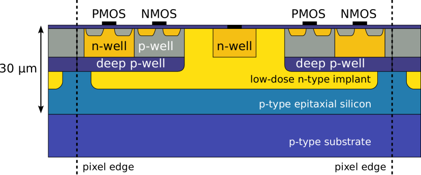
TJ-Monopix2 is a full scale \qtyproduct2x2\centi DMAPS prototype designed in \qty180\nano TowerSemiconductor444https://towersemi.com/ CMOS technology. Based on the ALPIDE pixel detector [6], its small collection electrode relative to the pixel pitch of \qtyproduct33.04x33.04\micro is separated from the in-pixel electronics, which are housed in p-wells at the pixel edges. The reduced sensor capacitance of accomplished by this design approach renders low analog power consumption of \qty∼1\micro and minimal noise operation at \qty∼5. The extended drift distances to the collection electrode and possible regions with low electric field expose the sensor to an increased probability of charge trapping after irradiation, making the sensor more susceptible to radiation damage. To reach the design target in radiation tolerance of \qty1e15≠ fluence, a low-dose n-implant beneath the collection electrode is implemented to ensure the uniformity of the electric field across the entire sensor [7, 8]. Previous studies have shown that an additional modification in form of a gap in the n-implant is needed to improve the lateral field shaping below the pixel corners after irradiation [9, 10, 11]. Figure 1 shows a schematic cross-section of a single pixel cell.
TJ-Monopix2 is equipped with the synchronous column-drain readout architecture developed for the FE-I3 readout chip [12]. A \qty7 gray encoded \qty40\mega counter (in the following referred to as BCID counter) is distributed along each double column. Upon a registered hit, the leading and trailing edge (LE/TE) of a discriminated signal is sampled on a pixel level for charge measurements via the time-over-threshold method. The corresponding \qty40\mega clock is internally derived from the \qty160\mega command clock in the chip’s periphery. Furthermore, each pixel contains a \qty3 local threshold DAC to minimize the threshold dispersion across the chip. A digital in-pixel injection circuitry is implemented to verify the general functionality of the analog front-end and readout architecture.
3 Cross Talk Analysis
Extensive tests of TJ-Monopix2 have verified improvements in threshold and equivalent noise charge (ENC) performance to its predecessor, TJ-Monopix1, in laboratory conditions [13]. Throughout the characterization, variations in the threshold response of TJ-Monopix2 were observed. To investigate this, the threshold was measured relative to a fixed time of arrival for all hits. The time of injection with respect to the BCID counter was shifted in steps of \qty3.125\nano by resetting the counter and adding an adjustable delay before every injection. A periodic pattern of the threshold distribution depending on the hit arrival time was observed, which is displayed in Figure 2 over an exemplary interval of the \qty7 counter. Red markers visualize the average threshold for each measurement point.
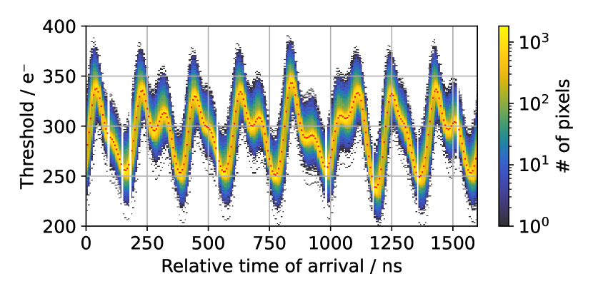
The measurement was conducted for initially tuned to a mean threshold of \qty260 with a dispersion of \qty6.555A conversion factor of \qty8.8 per injected charge DAC unit was applied corresponding to a calibration measurement utilizing Fe55 for this chip. Within the full BCID counter cycle, a maximum variation in mean threshold of about \qty105 was quantified, which exceeds the very good ENC performance of \qty7 by a factor of \qty15. Figure 3 shows a Fourier analysis of the periodic threshold pattern revealing a dominant frequency of \qty5\mega and a lesser noticeable \qty10\mega component.
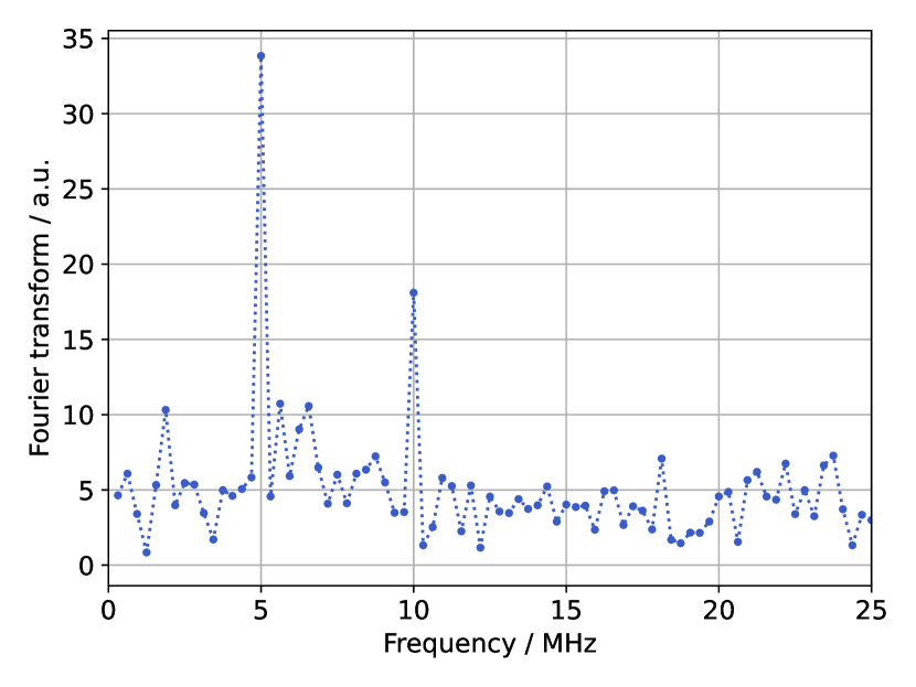
Due to the gray encoding used in the BCID counter, the observed frequencies are equal to the toggling frequency of the two least significant bits of the counter. Table 1 demonstrates the gray encoded counting method employing the first eight clock cycles, thereby illustrating the resulting toggling frequencies of \qty10\mega and \qty5\mega.
| LE/TE counter | ||
|---|---|---|
| Time | Decimal | Gray encoded |
| \qty0\nano | ||
| \qty25\nano | ||
| \qty50\nano | ||
| \qty75\nano | ||
| \qty100\nano | ||
| \qty125\nano | ||
| \qty150\nano | ||
| \qty175\nano | ||
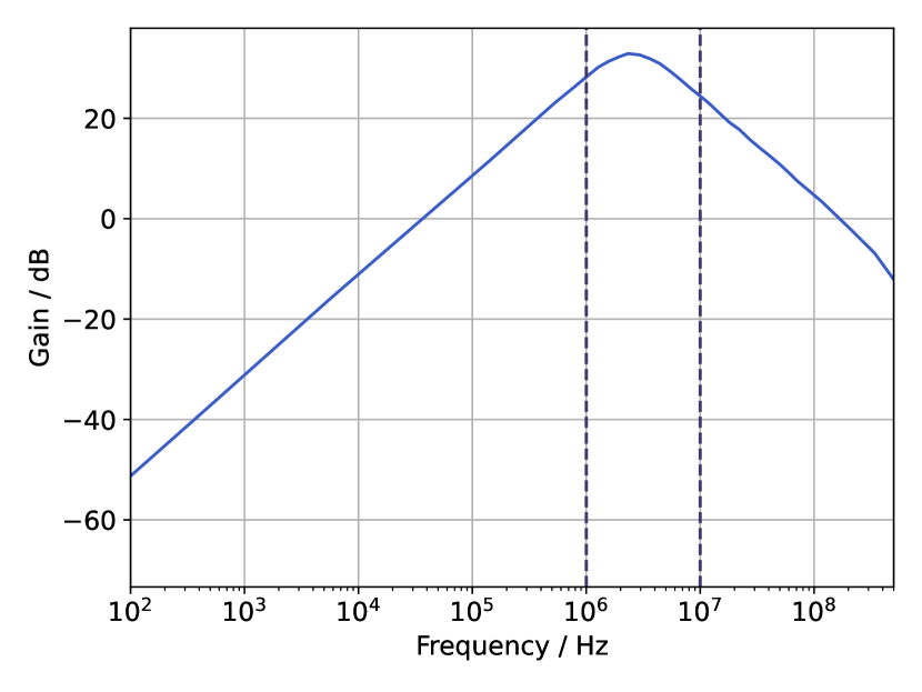
The simulated transfer function of the pre-amplifier implemented in TJ-Monopix2 is shown in Figure 4. The highest amplification is achieved for signals in the frequency range between \qtyrange110\mega [14]. Thus, the pre-amplifier facilitates potential cross-talk precisely in the range of frequencies corresponding to the toggling of the BCID counter bits.
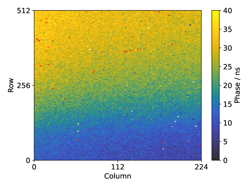
Furthermore, a delay in the threshold variation based on pixel position within the matrix was observed, arising from the influence of the BCID counter and injection pulse propagation time. To get an estimation of the local dependency, a simple sine function was fitted to the respective periodic pattern in threshold response for each pixel. The estimated phase of the threshold variation across the matrix is displayed in Figure 5, while frequency and amplitude of the variation remained similar for all pixels. Since the chip periphery and the end of column logic is situated at the bottom of the chip, the observed top to bottom gradient in the phase can be explained.
This gradient in the phase leads to variations in the threshold dispersion relative to the arrival time of hits. Figure 6 shows the evolution of the threshold dispersion over half of the maximum BCID counter interval. Originating from the combination of threshold variation frequency and phase shift, a periodic pattern in the threshold dispersion is visible. The dispersion reaches up to \qty20 in case of the most adverse phase difference between top and bottom pixels, surpassing the initial tuning result of \qty6 by more than threefold.

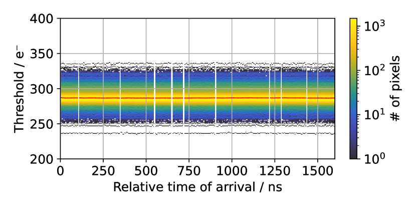
Disabling the distribution of the BCID counter across the matrix mitigated the threshold variation completely as shown in Figure 7. In the absence of leading edge (and charge) information for hits, the identical assignment of measurement points to a specific time of arrival as previously calibrated is employed. This proves the origin of the cross talk to arise from the distribution of the toggling BCID counter bits across the matrix.
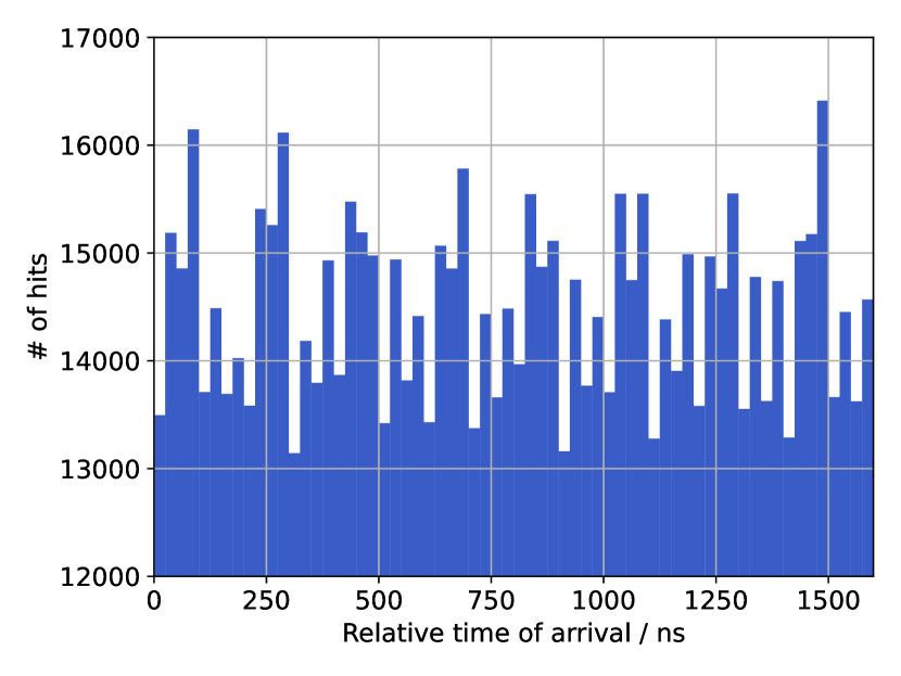
To better understand which part of the chip is affected by this cross talk, a measurement with a radioactive source was analyzed for the relative time of arrival of all detected hits. The resulting distribution over an exemplary segment of the complete BCID counter is shown in Figure 8. Analog to the observed threshold variation (Figure 2), a periodic pattern in the relative hit arrival time of non-injected hits was identified indicating an increased detection rate of hits at periods of lower thresholds. Consequently, this cross talk has no influence on the digital injection circuitry, but must impact the measured analog signal of a hit or the threshold level of the chip.
In an attempt to suppress the cross talk, the internally derived \qty40\mega clock was modulated by adjusting the command clock frequency to change the toggling frequency of the BCID counter bits. It was not possible to successfully suppress the threshold variation for a feasible command clock. In case of the deceleration of the clocks by a factor of four (yielding toggling frequencies of \qty2.5\mega and lower), a peak threshold fluctuation of \qty90 remained. Fourier analysis of the resulting curves resembled the respective change in toggling frequency of the counter bits within the sensitive pre-amplifier frequency range.
Upon closer investigation of the chip’s layout, the responsible distribution lanes of the BCID counter across the matrix were found to be well-shielded. Simulations of the chip’s matrix design are currently ongoing to better understand the origin of this phenomenon. For laboratory measurements, a predetermined delay between the reset of the BCID counter and the injection of a hit is used as a practical solution. However, this approach is not applicable for measurements where there is no control over the hit arrival time and energy information is wanted, such as radioactive source or beam tests.
4 Conclusion
The threshold performance of TJ-Monopix2 DMAPS prototypes was further investigated and a modulation of the threshold response relative to the hit arrival time was discovered. A maximum change of \qty105 in the periodic pattern of the mean threshold was quantified, exceeding the ENC performance of the chip by a factor of \qty15. Variations in threshold dispersion reaching up to three times the initial value after tuning were measured relative to the hit arrival time and followed the same periodic behavior. Execution of a Fourier analysis on the mean threshold oscillation revealed a dominant \qty5\mega frequency, matching the toggling frequency of the second least significant BCID counter bit. Analysis of measurements with a radioactive source has shown higher hit detection rates at periods of lower threshold, indicating that the cross talk affects either the analog signal of a hit or the threshold level of the chip. Mitigation of the threshold variation by disabling the BCID counter distribution across the matrix has proven that the cross talk is caused by the toggling of the counter bits. The constant phase relation between injection strobe and BCID counter, which is typically used for laboratory measurements, hides the now observed cross talk phenomenon. For a better understanding of this behavior, simulations of the chip matrix are still ongoing.
5 Acknowledgments
This project has received funding from the Deutsche Forschungsgemeinschaft DFG (grant WE 976/4-1), the German Federal Ministry of Education and Research BMBF (grant 05H15PDCA9), and the European Union’s Horizon 2020 research and innovation programme under grant agreements no. 675587 (Maria Sklodowska-Curie ITN STREAM), 654168 (AIDA-2020), and 101004761 (AIDAinnova).
References
- [1] R. Turchetta, et al., A monolithic active pixel sensor for charged particle tracking and imaging using standard VLSI CMOS technology, Nucl. Instrum. Meth. A 458 (2001) 677–689. doi:10.1016/S0168-9002(00)00893-7.
- [2] I. Peric, A novel monolithic pixelated particle detector implemented in high-voltage CMOS technology, Nucl. Instrum. Meth. A 582 (2007) 876–885. doi:10.1016/j.nima.2007.07.115.
- [3] M. Barbero, et al., Radiation hard DMAPS pixel sensors in 150 nm CMOS technology for operation at LHC, JINST 15 (05) (2020) 05. arXiv:1911.01119, doi:10.1088/1748-0221/15/05/P05013.
- [4] Technical Design Report for the ATLAS Inner Tracker Pixel Detector (2017). doi:10.17181/CERN.FOZZ.ZP3Q.
- [5] J. Dingfelder, et al., Progress in DMAPS developments and first tests of the Monopix2 chips in 150 nm LFoundry and 180 nm TowerJazz technology, Nucl. Instrum. Meth. A 1034 (2022) 166747. doi:10.1016/j.nima.2022.166747.
- [6] M. Mager, ALPIDE, the Monolithic Active Pixel Sensor for the ALICE ITS upgrade, Nucl. Instrum. Meth. A 824 (2016) 434–438. doi:10.1016/j.nima.2015.09.057.
- [7] W. Snoeys, et al., A process modification for CMOS monolithic active pixel sensors for enhanced depletion, timing performance and radiation tolerance, Nucl. Instrum. Meth. A 871 (2017) 90–96. doi:10.1016/j.nima.2017.07.046.
- [8] H. Pernegger, et al., Radiation hard monolithic CMOS sensors with small electrodes for High Luminosity LHC, Nucl. Instrum. Meth. A 986 (2021) 164381. doi:10.1016/j.nima.2020.164381.
- [9] I. Caicedo, et al., The Monopix chips: Depleted monolithic active pixel sensors with a column-drain read-out architecture for the ATLAS Inner Tracker upgrade, JINST 14 (06) (2019) C06006. doi:10.1088/1748-0221/14/06/C06006.
- [10] C. Bespin, et al., DMAPS Monopix developments in large and small electrode designs, Nucl. Instrum. Meth. A 978 (2020) 164460. doi:10.1016/j.nima.2020.164460.
- [11] M. Dyndal, et al., Mini-malta: radiation hard pixel designs for small-electrode monolithic cmos sensors for the high luminosity lhc, Journal of Instrumentation 15 (02) (2020) P02005–P02005. doi:10.1088/1748-0221/15/02/p02005.
- [12] I. Peric, L. Blanquart, G. Comes, P. Denes, K. Einsweiler, P. Fischer, E. Mandelli, G. J. Meddeler, The FEI3 readout chip for the ATLAS pixel detector, Nucl. Instrum. Meth. A 565 (2006) 178–187. doi:10.1016/j.nima.2006.05.032.
- [13] C. Bespin, et al., Charge collection and efficiency measurements of the TJ-Monopix2 DMAPS in 180 nm CMOS technology, PoS Pixel2022 (2023) 080. doi:10.22323/1.420.0080.
-
[14]
Konstantinos Moustakas, Design and development of depleted monolithic active pixel sensors with small collection electrode for high-radiation applications, Ph.D. thesis, Rheinische Friedrich-Wilhelms-Universität Bonn (Sep. 2021).
URL https://hdl.handle.net/20.500.11811/9315