[1,2,3]\fnmM. \surFaverzani \equalcontThese authors contributed equally to this work. \equalcontThese authors contributed equally to this work. \equalcontThese authors contributed equally to this work. \equalcontThese authors contributed equally to this work.
1]\orgdivPhysics Department, \orgnameUniversity of Milano - Bicocca, \orgaddress\cityMilano, \countryItaly 2]\orgnameINFN Sezione di Milano - Bicocca, \orgaddress\cityMilano, \countryItaly 3]\orgnameBicocca Quantum Technologies (BiQuTe) Centre, \orgaddress\cityMilano, \countryItaly 4]\orgnameFondazione Bruno Kessler, \orgaddress\cityTrento, \countryItaly 5]\orgnameINFN - TIFPA, \orgaddress\cityTrento, \countryItaly 6]\orgdivPhysics Department \orgnameUniversity of Salerno, \orgaddress\citySalerno, \countryItaly 7]\orgnameINFN Sezione di Napoli, \orgaddress\cityNapoli, \countryItaly 8]\orgdivPhysics Department \orgnameUniversity of Salento, \orgaddress\cityLecce, \countryItaly 9]\orgnameINFN Sezione di Lecce, \orgaddress\cityLecce, \countryItaly 10]\orgnameINRiM, \orgaddress\cityTorino, \countryItaly 11]\orgnameINO-CNR BEC Center, \orgaddress\cityTrento, \countryItaly 12]\orgdivPhysics Department \orgnameUniversity of Trento, \orgaddress\cityTrento, \countryItaly 13]\orgnameINFN Laboratori Nazionali di Frascati, \orgaddress\cityFrascati, \countryItaly 14]\orgnameIFN-CNR, \orgaddress\cityTrento, \countryItaly 15]\orgdivDepartment of Science and Technology \orgnameUniversity of Sannio, \orgaddress\cityBenevento, \countryItaly
Broadband parametric amplification in DARTWARS
Abstract
Superconducting parametric amplifiers offer the capability to amplify feeble signals with extremely low levels of added noise, potentially reaching quantum-limited amplification. This characteristic makes them essential components in the realm of high-fidelity quantum computing and serves to propel advancements in the field of quantum sensing. In particular, Traveling-Wave Parametric Amplifiers (TWPAs) may be especially suitable for practical applications due to their multi-Gigahertz amplification bandwidth, a feature lacking in Josephson Parametric Amplifiers (JPAs), despite the latter being a more established technology. This paper presents recent developments of the DARTWARS (Detector Array Readout with Traveling Wave AmplifieRS) project, focusing on the latest prototypes of Kinetic Inductance TWPAs (KITWPAs). The project aims to develop a KITWPA capable of achieving dB of amplification. To enhance the production yield, the first prototypes were fabricated with half the length and expected gain of the final device. In this paper, we present the results of the characterization of one of the half-length prototypes. The measurements revealed an average amplification of approximately dB across a GHz bandwidth for a KITWPA spanning mm in length.
keywords:
Quantum noise, parametric amplifier, traveling wave, detector array readout, qubits readout1 Introduction
The rapid evolution of quantum computing demands for amplifiers featuring wide bandwidth, large dynamic range, and quantum-limited added noise. Devices with these characteristics would also offer significant advantages to quantum sensing for the readout of low-temperature detectors, ultimately enhancing the performance of next-generation experiments.
Superconducting parametric amplifiers exploit a non-linear circuit to amplify signals. Among these devices, Josephson Parametric Amplifiers (JPAs) [1] stand out as the best-established technology. While JPAs have demonstrated their ability to achieve quantum-limited noise performances, they are constrained by other limitations, primarily associated with their relatively narrow bandwidth and limited dynamic range of amplification.
Another class of devices comprises Traveling Wave Parametric Amplifiers (TWPAs), which have the potential to expand the bandwidth and dynamic range to values close to the ones of existing standard commercial amplifiers. A TWPA features a non-linear transmission line that is either embedded with Josephson junctions (TWJPA) [2] or made with high-kinetic inductance materials (KITWPA) [3]. Both of these approaches are being pursued [4, 5, 6, 7, 8] by the DARTWARS (Detector Array Readout with Traveling Wave AmplifieRS) project, which aims to reach gain, noise and saturation power of around dB, mK, and dBm respectively.
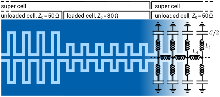
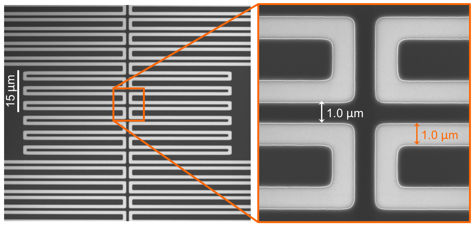
This paper focuses on the latest developments of DARTWARS, providing a more comprehensive characterization of the KITWPA prototypes introduced in [9], which demonstrated significant amplification in preliminary tests. A KITWPA consists of a weakly dispersive phase-matched transmission line, controlled by dispersion engineering, which is required to create exponential amplification [10]. The prototype characterized in this paper is an artificial transmission line organized in multiple cells, each one composed of a stub-loaded coplanar waveguide (CPW) with an inductance () dependent on the kinetic inductance of the material and two interdigitated capacitors (IDC) to establish capacitance () towards the ground. Dispersion engineering was achieved by organizing the transmission line into super-cells, each comprising unloaded cells with a characteristic impedance , and loaded cells with , for a total of cells in each supercell (fig. 2).
The mm transmission line length corresponds to an expected amplification of approximately dB. The design of the KITWPAs was optimized to produce these devices with a bandwidth centered at GHz. The next fabrication will produce devices with a higher ratio of loaded to unloaded cells, shifting the bandwidth center up to GHz. The KITWPAs were produced by depositing a thin film of NbTiN on a high-resistivity silicon wafer (fig. 2). Further details on the fabrication process are reported in [9].
2 Characterization of the KITWPA prototype
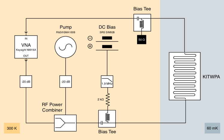
In the present work, one of the devices with mA and a clearly identifiable stop-band was selected for low-temperature characterization at mK. The experimental setup shown in fig. 3 was used to scan the response of the TWPA while controlling its dc bias and pump signal. The instruments used for performing the characterization were controlled using the Qtics Python package [11]. The KITWPA chip was mounted in a general-purpose copper box, equipped with CPW launchers to feed the device.
2.1 Measurement of non-linearity parameters
At the lowest order, the inductance of the KITWPA increases quadratically as a function of the dc bias . This non-linear response can be measured by considering the phase of the parameter at a fixed frequency :
| (1) |
where is the phase at zero bias, while is an intrinsic parameter of the material known as the scaling current. Finally, represents the phase delay over the entire transmission line.
The time required by a signal to travel across the device ns was measured with a Time-Domain-Reflectometer (TDR). This allowed to estimate the phase delay and the phase velocity . The latter was also cross-checked with an alternative estimate based on the relation , where and GHz refer respectively to the wavelength corresponding to the spatial separation between subsequent periodic loadings and the central frequency of the measured stop-band. These approaches yielded a phase-velocity of () and () respectively, demonstrating consistent results between the two techniques.
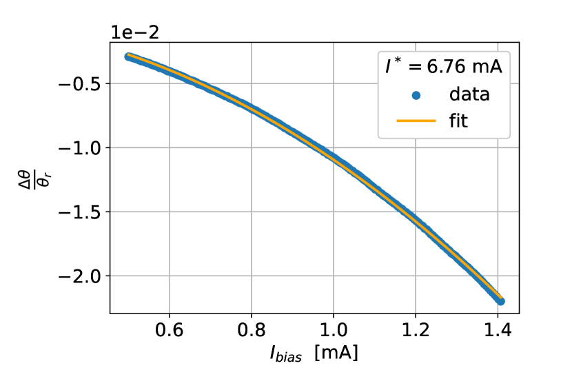
To measure the scaling current , the data were acquired by recording the response with the VNA for various dc bias values while keeping the rf pump turned off. As shown in fig. 5, fitting the measured and rescaled phase at a fixed frequency with eq. 1 allows to determine . Repeating the fit for different frequencies over the whole amplification bandwidth resulted in an average value of mA, where the uncertainty was estimated as the standard deviation of the fit results.
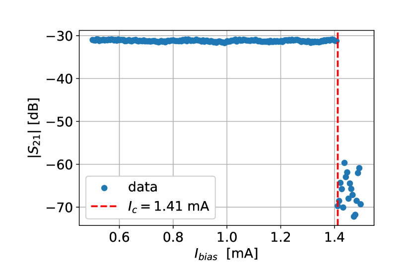
The critical current of the device was instead measured by considering the amplitude of as a function of the dc bias. For a fixed frequency, can be easily identified as a significant discontinuity in the transmitted VNA signal amplitude (fig. 5). Consistent values of were found when considering different frequencies across the entire amplification bandwidth, resulting in mA.
In a preliminary characterization [9], another batch of prototypes was tested in liquid helium, which led to a measured scaling and critical currents of mA and mA respectively. Comparing these measurements with our device, the critical currents are in good agreement while the scale currents have slightly different values, but still maintain the same order of magnitude.
2.2 Gain measurements
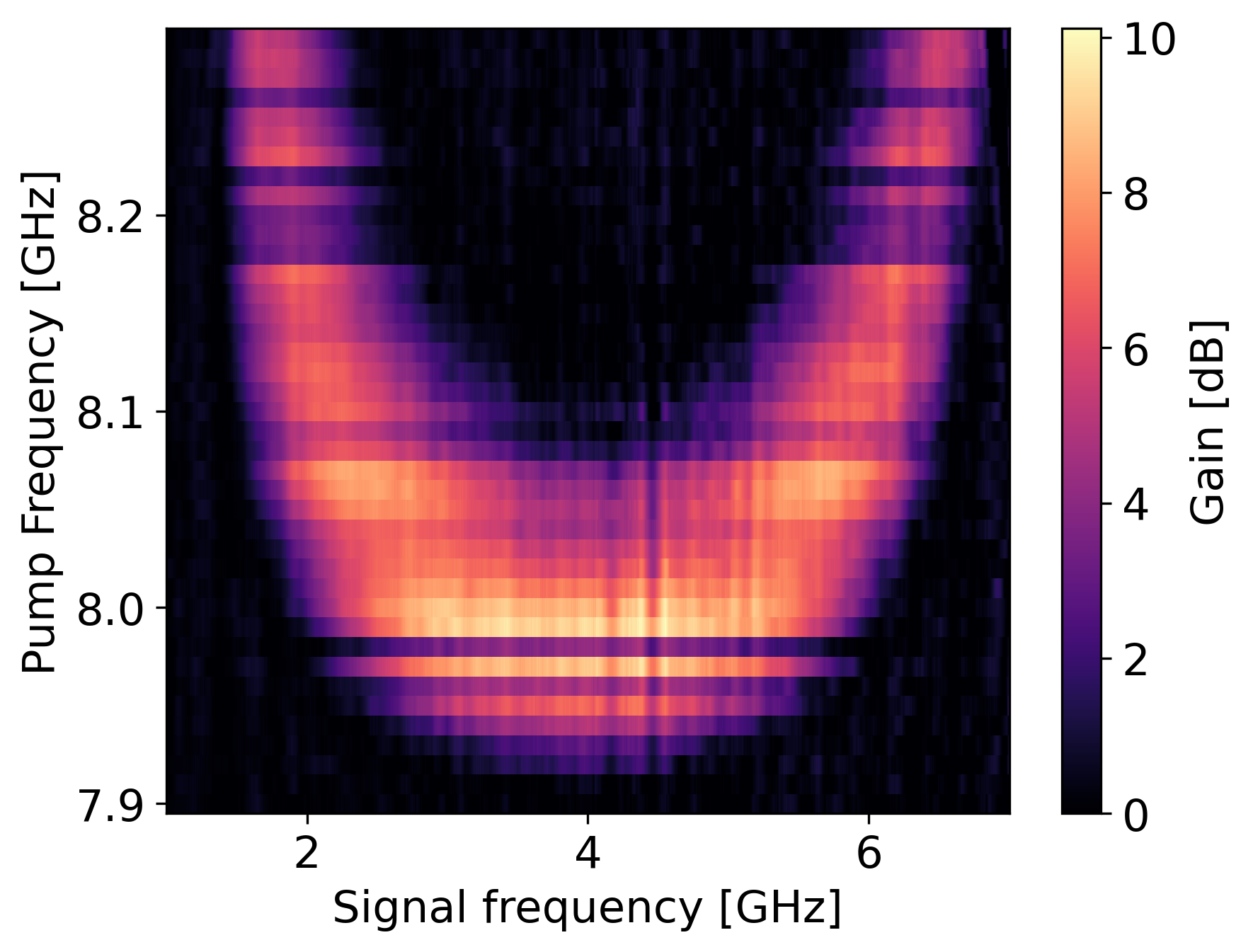
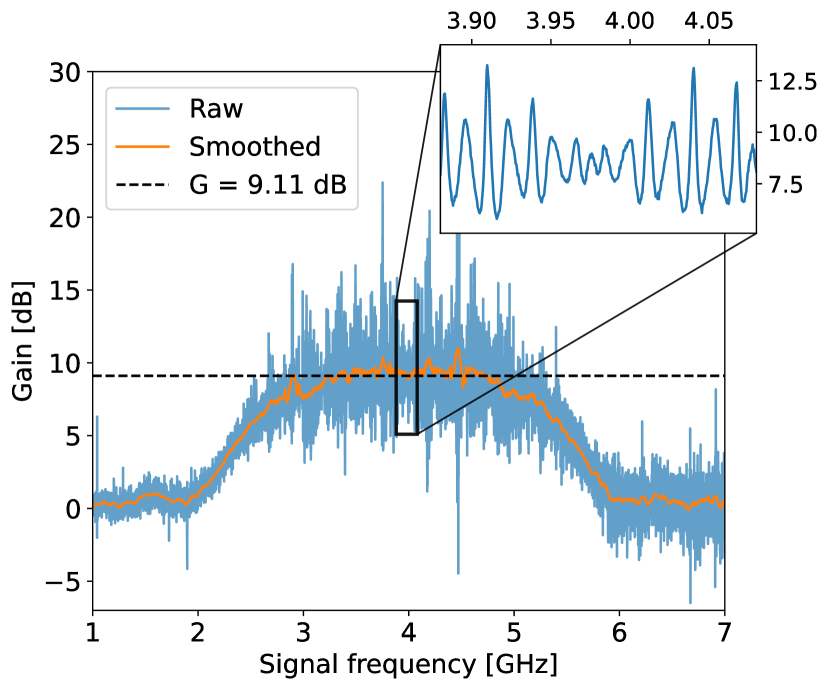
The best gain and corresponding bandwidth were characterized through a VNA frequency sweep in the GHz range, while varying the pump rf signal within the GHz range, which is just above the stop-band. Additional parameters, such as the dc biasing current or the pump power, were fine-tuned separately to mA and dBm. In fig. 7, the measured gain is plotted as a function of the VNA and the pump rf signals frequencies. As predicted by the phase-matching relations [12], a splitting of the bandwidth becomes apparent as the pump rf signal frequency increases. A mean gain of dB was achieved over a GHz range at a pump rf signal frequency of GHz (fig. 7). However, the gain does not appear to be uniform due to large ripples (inset in fig. 7). By performing a Fast Fourier Transform (FFT) of the transmitted signal, it can be seen that the dominant frequency corresponds to a wavelength approximately twice the length of the device. This explains the ripples as resulting from impedance mismatches introduced by the line adaptation and connections between the KITWPA and the packaging, which lead to the creation of standing waves across the device.
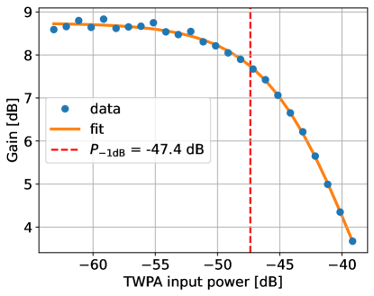
The final measurements focused on assessing the power handling capabilities of the device. While keeping the pump and dc bias parameters fixed, the mean gain was evaluated as a function of the VNA rf signal power injected into the TWPA. While the gain remains constant for low VNA powers, an increase in power causes the TWPA to saturate its output, leading to a gradual degradation of the gain. It is common to extract the dB compression point, which is identified as the input power necessary to deviate by dB from the maximum stable gain. The measured mean gain as a function of the TWPA input power is shown in fig. 8. A value of dB was obtained considering the mean gain in the GHz frequency range, which demonstrates the significant power handling capabilities of these devices with respect to other parametric amplifiers.
3 Conclusions
This paper presented the latest developments of the DARTWARS project, regarding the advancements of KITWPAs for applications in quantum computing and sensing. We characterized one of the latest prototypes at cryogenic temperatures (mK) and measured a maximum mean gain of dB in the frequency range from to GHz. The examined device exhibited a critical current of mA and a scaling current of mA, with its dB compression point estimated at dB. The measured values are in reasonable agreement with the design goals of the prototype. Future phases of the project will involve noise performance characterization, producing additional short prototypes with an amplification bandwidth centered at higher frequencies, and eventually fabricating full-length devices with dB of amplification.
Acknowledgement
This work is supported by DARTWARS, a project funded by the Italian Institute of Nuclear Physics (INFN) within the Technological and Interdisciplinary Research Commission (CSN5), by European Union’s H2020-MSCA Grant Agreement No. 101027746, by the Italian National Centre for HPC Big Data and Quantum Computing (PNRR MUR project CN0000013-ICSC) and by the Italian National Quantum Science and Technology Institute (PNRR MUR project PE0000023-NQSTI). We acknowledge the support of the FBK cleanroom team for the fabrication. We also acknowledge useful discussions with Jiansong Gao, Michael Vissers, Jordan Wheeler, and Maxime Malnou. CB and SP acknowledge support from University of Salerno - Italy under the projects FRB19PAGAN, FRB20BARON and FRB22PAGAN.
References
- \bibcommenthead
- Castellanos-Beltran et al. [2008] Castellanos-Beltran, M.A., Irwin, K.D., Hilton, G.C., Vale, L.R., Lehnert, K.W.: Amplification and squeezing of quantum noise with a tunable Josephson metamaterial. Nature Physics 4, 929 (2008) https://doi.org/10.1038/nphys1090
- Macklin et al. [2015] Macklin, C., et al.: A near quantum-limited Josephson traveling-wave parametric amplifier. Science 350(6258), 307–310 (2015) https://doi.org/10.1126/science.aaa8525
- Ho Eom et al. [2012] Ho Eom, B., et al.: A wideband, low-noise superconducting amplifier with high dynamic range. Nature Physics 8(8), 623–627 (2012) https://doi.org/10.1038/nphys2356
- Borghesi et al. [2023] Borghesi, M., et al.: Progress in the development of a KITWPA for the DARTWARS project. Nucl. Instrum. Meth. A 1047, 167745 (2023) https://doi.org/10.1016/j.nima.2022.167745 arXiv:2208.10101 [quant-ph]
- Rettaroli et al. [2023] Rettaroli, A., et al.: Ultra low noise readout with traveling wave parametric amplifiers: The DARTWARS project. Nucl. Instrum. Meth. A 1046, 167679 (2023) https://doi.org/10.1016/j.nima.2022.167679 arXiv:2207.12775 [quant-ph]
- Pagano et al. [2022] Pagano, S., et al.: Development of Quantum Limited Superconducting Amplifiers for Advanced Detection. IEEE Transactions on Applied Superconductivity 32(4), 1–5 (2022) https://doi.org/10.1109/TASC.2022.3145782
- Granata et al. [2023] Granata, V., et al.: Characterization of Traveling-Wave Josephson Parametric Amplifiers at T = 0.3 K. IEEE Transactions on Applied Superconductivity 33(1), 1–7 (2023) https://doi.org/10.1109/TASC.2022.3214656
- Guarcello et al. [2023] Guarcello, C., et al.: Modeling of josephson traveling wave parametric amplifiers. IEEE Transactions on Applied Superconductivity 33(1), 1–7 (2023) https://doi.org/10.1109/TASC.2022.3214751
- Mantegazzini et al. [2023] Mantegazzini, F., et al.: High kinetic inductance NbTiN films for quantum limited travelling wave parametric amplifiers. Physica Scripta 98(12), 125921 (2023) https://doi.org/10.1088/1402-4896/ad070d
- Chaudhuri et al. [2017] Chaudhuri, S., et al.: Broadband parametric amplifiers based on nonlinear kinetic inductance artificial transmission lines. Applied Physics Letters 110(15), 152601 (2017) https://doi.org/10.1063/1.4980102
- Carobene et al. [2024] Carobene, R., Campana, P., Gobbo, M., Giachero, A.: Qtics - Quantum Technologies Instrumentation ControlS (Version 0.0.2) (2024) https://doi.org/10.5281/zenodo.10450507
- Malnou et al. [2021] Malnou, M., Vissers, M.R., Wheeler, J.D., Aumentado, J., Hubmayr, J., Ullom, J.N., Gao, J.: Three-Wave Mixing Kinetic Inductance Traveling-Wave Amplifier with Near-Quantum-Limited Noise Performance. PRX Quantum 2, 010302 (2021) https://doi.org/10.1103/PRXQuantum.2.010302