Graphene Terahertz Technology
Abstract
During the past two decades, a variety of linear and nonlinear dynamical phenomena, especially in the terahertz (THz) frequency range, have been revealed for charge carriers in graphene, which can be utilized to develop THz devices – i.e., emitters, receivers, and modulators of THz electromagnetic waves. This review discusses various applications of graphene in THz technology, including sensing, spectroscopy, photonics, and communications. First, the basic physics and techniques of THz-wave absorption processes in graphene are discussed. THz wave absorption in graphene can occur both through interband and intraband absorption processes. Such absorption can be readily modulated by an applied gate voltage and can be enhanced by utilizing parallel-plate waveguides or a total internal reflection geometry. Next, the effect of adsorbed molecules on THz emission from graphene is described. This phenomenon can be used to construct a metamaterial-free THz sensor for biointerfaces. The manipulation of THz waves through thermal annealing is also discussed, as well as their enhancement in a graphene-based THz modulator employing metallic ring apertures. Lastly, the review highlights the excitation of propagating surface plasmon polaritons in graphene at THz frequencies, which can play important roles in THz devices for communications, nanophotonics, and imaging.
keywords:
Graphene, 2D materials, Terahertz spectroscopy, THz wave modulation, Surfaceplasmon polariton, Molecular sensing
Anna-Christina Samaha, Jacques Doumani, T. Elijah Kritzell, Andrey Baydin, Pulickel M. Ajayan, Mario El Tahchi, Junichiro Kono*
Anna-Christina Samaha and Prof. Mario El Tahchi
Laboratory of Biomaterials and Intelligent Materials, Department of Physics, Faculty of Sciences 2, Lebanese University, P.O. Box 90656, Jdeidet, Lebanon
annachristina.samaha@st.ul.edu.lb and mtahchi@ul.edu.lb
Jacques Doumani and T. Elijah Kritzell
Department of Electrical and Computer Engineering, Rice University, 6100 Main Street, Houston, TX 77005, USA
Applied Physics Graduate Program, Smalley–Curl Institute, Rice University, 6100 Main Street,
Houston, TX 77005, USA
jd74@rice.edu and tek3@rice.edu
Dr. Andrey Baydin
Department of Electrical and Computer Engineering, Rice University, 6100 Main Street, Houston, TX 77005, USA
Smalley–Curl Institute, Rice University, 6100 Main Street, Houston, TX 77005, USA
baydin@rice.edu
Prof. Pulickel M. Ajayan
Department of Materials Science and NanoEngineering, Rice University, 6100 Main Street,
Houston, TX 77005, USA
Smalley–Curl Institute, Rice University, 6100 Main Street, Houston, TX 77005, USA
pma2@rice.edu
Prof. Junichiro Kono
Department of Electrical and Computer Engineering, Rice University, 6100 Main Street, Houston, TX 77005, USA
Smalley–Curl Institute, Rice University, 6100 Main Street, Houston, TX 77005, USA
Department of Physics and Astronomy, Rice University, 6100 Main Street, Houston, TX 77005, USA
Department of Materials Science and NanoEngineering, Rice University, 6100 Main Street,
Houston, TX 77005, USA
Carbon Hub, Rice University, 6100 Main Street, Houston, TX 77005, USA
kono@rice.edu
1 Introduction
Graphene is a distinctive two-dimensional (2D) material comprising a honeycomb lattice structure formed by a single layer of -bonded carbon atoms. This material has been the focus of intensive research due to its exceptional mechanical, electrical, optical, and thermal properties [1, 2, 3, 4, 5, 6, 7]. Graphene is considered one of the most robust materials, with a tensile strength that is 200 times greater than that of steel [8]. Additionally, it is an excellent conductor of electricity, with electrical conductivity that is 1000 times greater than copper [9]. Furthermore, graphene has a thermal conductivity that exceeds diamond’s [10]. Due to these remarkable properties, graphene has the potential to revolutionize various fields, including electronics [11], photonics [12], energy storage [13], and biomedicine [14].
Due to the gapless Dirac-cone band structure, carriers in graphene exhibit ultrahigh electron mobilities and strong nonlinear response to electromagnetic fields [15]. Across an extensive spectral range, a myriad of optical phenomena have been explored in graphene to date: excitonic [16], plasmonic [17], nonlinearity including second-harmonic [18], third-harmonic [19] and high-harmonic generation [20], Fano resonances [21], and circular dichroism [22]. In particular, linear gapless bands near the Dirac point allow excitation of charge carriers by low-energy photons, i.e., terahertz (THz) radiation [15, 23, 24, 25]. The THz frequency range is usually defined as the range between 0.1 THz and 10 THz. It falls between the microwave and infrared frequency bands, represented by the electronic and photonic regimes, respectively [26, 27, 28], and commonly referred to as the “THz technology gap” due to the limited number of practical technologies for generating and detecting THz radiation [28, 29]. THz waves can penetrate various materials, providing spectral fingerprints that identify molecular structures. This unique characteristic renders THz radiation an invaluable tool for various applications, from chemical sensing to medical imaging [30].
Graphene, with its distinct electronic properties mentioned above, is considered one of the most ideal candidates for filling the THz technology gap [15]. Both interband and intraband optical transitions contribute to the optical conductivity of graphene, but the latter is particularly significant at THz frequencies. Intraband transitions, or free carrier absorption, are essential for both the equilibrium and photoexcited states and significantly affect the material’s response to THz radiation. Recent studies [15, 31, 32, 33, 34, 35, 36] have contributed crucial insights into the intricate dynamics of intraband transitions in graphene at THz frequencies, which lay the groundwork for exploiting graphene’s capabilities in the development of devices for the generation, detection, and modulation of THz radiation [37, 5, 38, 25].
This review explores various applications of graphene with THz radiation. First, we focus on carrier dynamics as probed by THz spectroscopy, highlighting the Fermi-level-dependent response and low-density detection with THz parallel-plate waveguides. Then, we move on to molecular sensing applications of graphene. The electrical properties of graphene are sensitive to the adsorbed molecules and, therefore, result in changes in the THz optical conductivity. Moreover, the detection of adsorbed molecules via THz emission spectroscopy is also discussed. Finally, gate-controlled THz wave manipulation and surface plasmon polaritons in graphene-based devices are presented. Based on the knowledge accumulated in the literature, we conclude that graphene is poised to revolutionize THz technology, offering opportunities for innovation and advancement.
2 Probing Carriers in Graphene with THz Spectroscopy
Understanding carrier dynamics in graphene is paramount for its optoelectronic applications. Ultrafast pump-probe spectroscopies, time-resolved Raman spectroscopy, and measurements of photocurrent have all been useful in revealing insights into electron-electron, electron-phonon, and phonon-phonon interactions [39, 40, 41, 42, 43, 44, 45, 46, 47, 48, 49, 50]. Both intraband and interband contributions to the optical conductivity of graphene have been probed via a variety of steady-state and transient spectroscopy methods [51, 52, 53, 54, 55, 56, 57, 58, 41, 59, 60, 61, 62, 36, 49, 63, 64, 65]. THz spectroscopy, in particular, plays a crucial role in characterizing carrier dynamics, offering deep insights into the properties of materials [66, 67, 68, 33, 69, 70]. This sensitive approach not only enhances our understanding of carrier behavior but also contributes to the advancement of graphene-based technologies.
2.1 Gate Control of THz Wave Transmission through Graphene
Since the position of the Fermi energy, , influences intraband and interband transitions [36, 33], carrier-density-dependent spectroscopy is particularly useful. The changes in carrier density can be sensitively monitored through THz time-domain spectroscopy (THz-TDS) or Fourier-transform infrared (FTIR) spectroscopy [71, 72, 73]. One way to tune is through chemical doping, but replacing carbon atoms in graphene with other elements suppresses the mobility [74, 75]. Consequently, the most effective method for tuning is by implementing a variable gate voltage, .
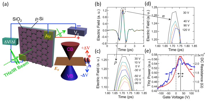
Figure 1(a) shows a large-area (centimeter-sized) field-effect transistor, consisting of monolayer graphene on a SiO2/-Si substrate [35, 76]. The electrodes laying on top of graphene and on the backside of the -Si substrate, respectively, are connected to a DC voltage supply, and simultaneously, a lock-in amplifier is employed to monitor the DC conductance (or resistance) of the graphene layer [77]. A THz electromagnetic wave is normally incident onto the sample, and its transmitted intensity changes based on the gate voltage, , applied between the graphene layer and the Si substrate. As depicted in Figure 1(b), the highest THz transmission is obtained at 30 V when the Fermi energy reaches the charge neutrality point. For voltages below and above this value, there is a monotonic decrease in THz transmission with the voltage variation, as illustrated in Figure 1(c-d). Figure 1(e) shows the transmitted THz beam power (blue circled line) alongside the DC resistance (red trace) versus . A maximum DC resistance is observed at 30 V, demonstrating conformity with the gate dependence of the transmitted THz power, which peaks at this voltage. Thus, this work clearly demonstrates that gated large-area graphene samples are useful for manipulating THz transmission by tuning [35, 77].
2.2 Detecting Low-Density Carriers in Graphene Using THz Parallel-Plate Waveguides
Studying the THz response of thin materials like monolayer graphene can be challenging due to their short interaction length with THz radiation. As discussed in Section 2.1, increasing the carrier density by applying a gate voltage to graphene can enhance its response to THz radiation [77], but this technique necessitates gate electrodes and is not always applicable to common 2D materials. Moreover, the influence of gate-induced carriers on the substrate must be considered.
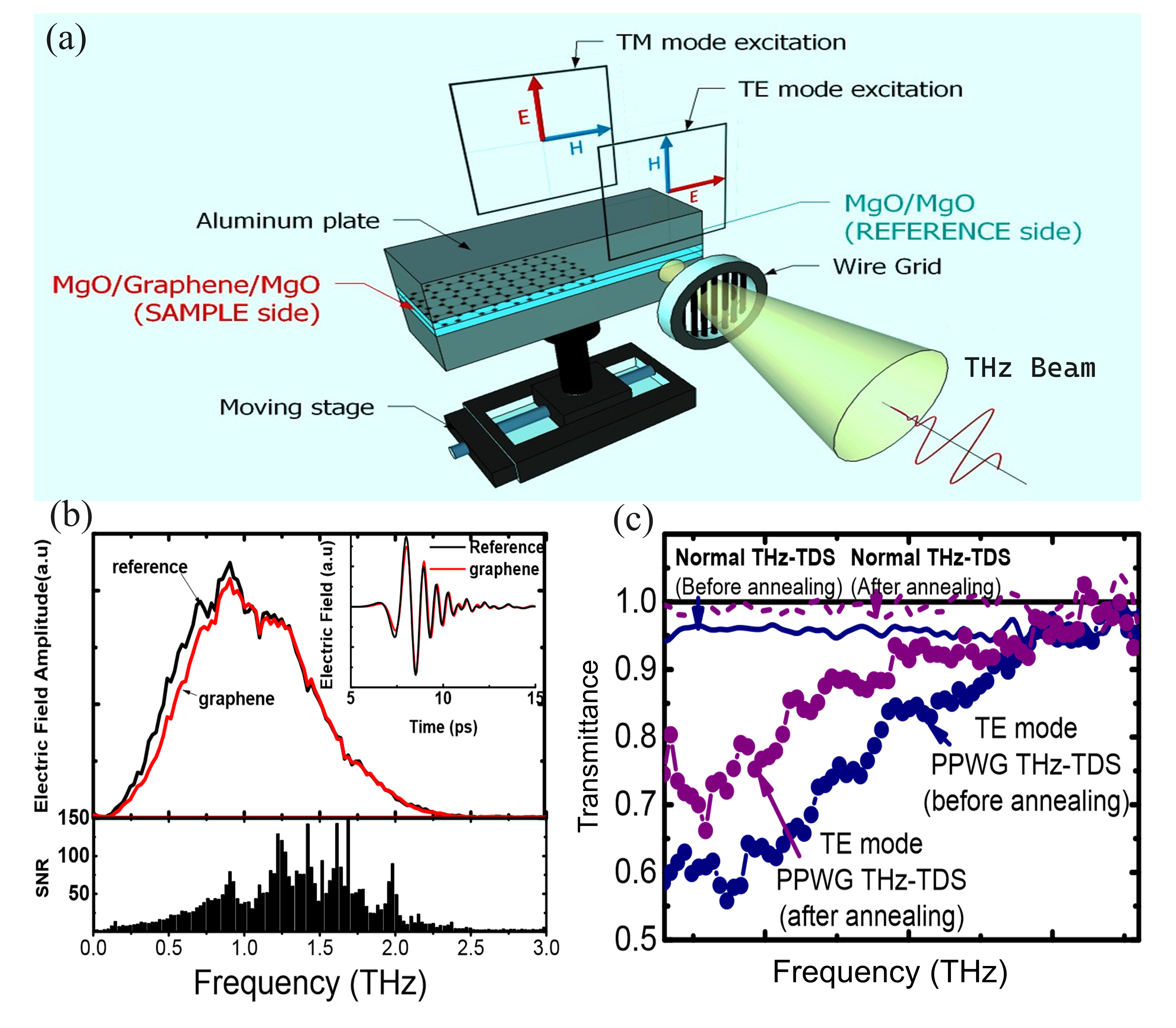
Another way to achieve a better response is to insert graphene into a parallel-plate waveguide (PPWG). This configuration provides a longer interaction length than the conventional THz spectroscopy, resulting in higher sensitivity. Additionally, this method facilitates the detection of the behavior of 2D materials in response to diverse polarizations of the electromagnetic field through waveguide mode control [79, 78, 80]. A waveguide structure typically used in the PPWG scheme [78] is illustrated in Figure 2(a), which consists of two aluminum plates. In the first half of the PPWG, chemical vapor deposition (CVD) grown graphene is inserted between two THz-transparent MgO substrates. In the other half, bare MgO substrates are used as a reference. A linear polarizer is set before the waveguide to provide - or -polarization configurations, allowing the excitation of either the transverse electric (TE) or transverse magnetic (TM) mode [79, 78].
THz spectra obtained for both the reference and the graphene sample are illustrated in Figure 2(b), with the THz wave polarized in the TE mode, while the inset shows the corresponding time-domain THz waveforms. For PPWG THZ-TDS, the alignment of the waveguide greatly contributes to the accuracy of the data. Therefore, THz pulses for the sample and the reference are recorded for ten different locations each. The signal-to-noise ratio (SNR) is calculated by dividing the average amplitude of the THz spectrum by its standard deviation [81]. Figure 2(c) presents a comparison of the transmittance spectra between conventional THz-TDS and PPWG THz-TDS for monolayer graphene, before and after annealing. In conventional THz-TDS, the spectra remain almost flat across the frequency range, with transmittance values of 95%, both before and after annealing. On the other hand, the spectra obtained with PPWG THz-TDS show variations in transmittance depending on the frequency. In the low-frequency regions, the transmittance is 60% before annealing, and 70% after annealing. These values increase to 95% at the end of the spectra for high frequencies. Hence, using PPWG THz-TDS results in a 30% decrease in transmission for graphene, which has a low-density carrier (2 1011 cm-2), showing the advantage of this method, while the conventional method was blind to any substantial carrier density change.
2.3 Enhancing THz Absorption through Total Internal Reflection
An alternative method for enhancing THz absorption in graphene is using a total internal reflection (TIR) geometry [82], where the absorption of electromagnetic waves can be tuned between 100% and 0% by changing the of graphene [83, 84]. Enhanced modulation depth in the THz regime has been achieved using a wire grating and ionic gel-based graphene TIR THz modulators [85, 86]. The geometry used in [84] consists of a large-area graphene sample inserted between two dielectric media. One of the chosen dielectric media is thermoplastic olefin polymer of amorphous structure (TOPAS), with a refractive index ( = 1.523 0.002) and a negligible absorption across all the THz range [87, 88, 89], while the other is air ( = 1). To satisfy the TIR condition, the THz wave must have an angle of incidence greater than the critical angle (), and according to Snell’s law, .
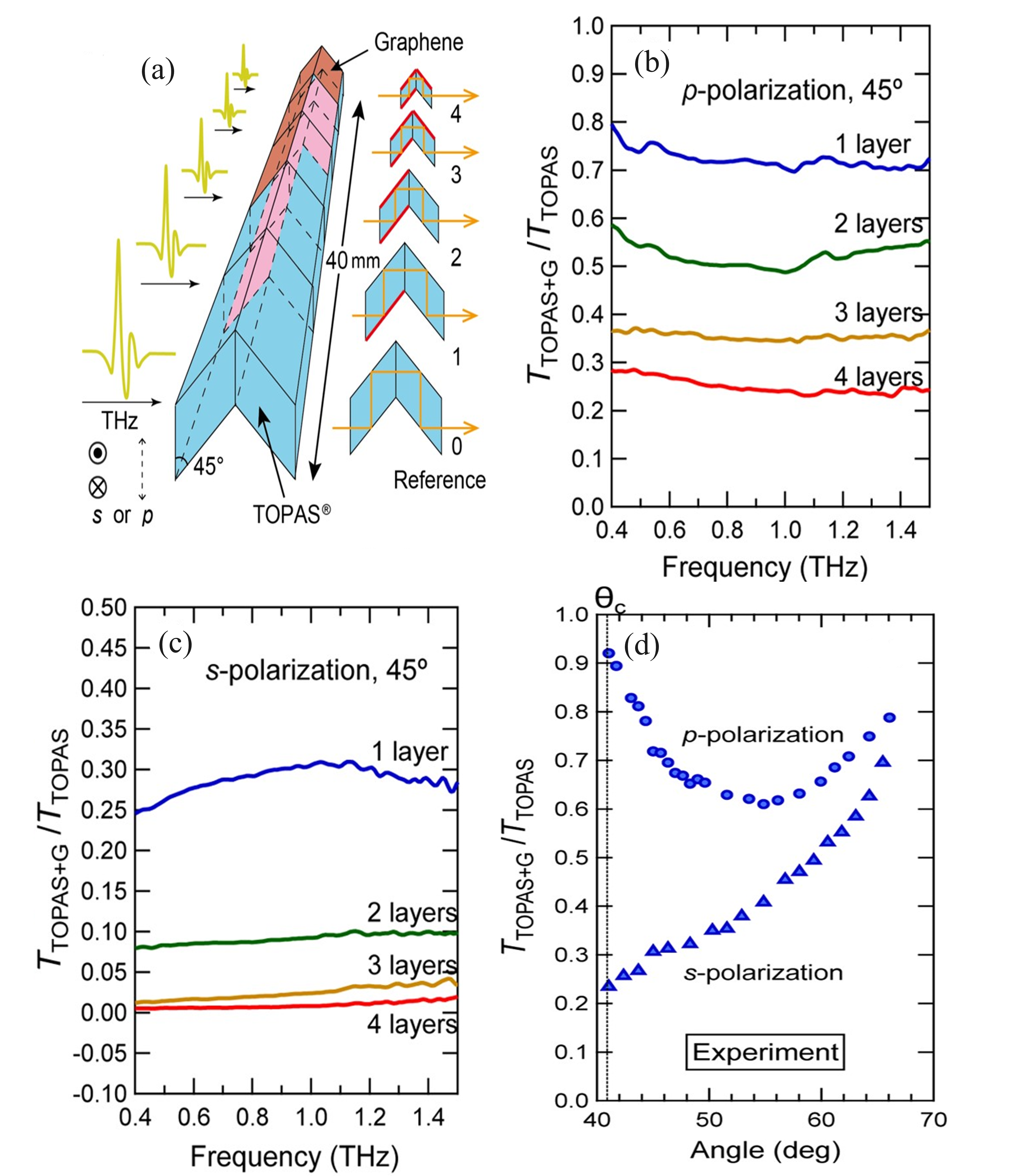
The design of the “graphene-on-TOPAS” waveguide is schematically shown in Figure 3(a). Two parallelogram-shaped TOPAS are combined to form a prism with six TOPAS/air interfaces. While two of the facets are left graphene-free (one for receiving the incident THz beam and the other for transmitting it), a specific number of the remaining four interfaces are covered with graphene. This is done to measure the transmittance for cases involving 0, 1, 2, 3, and 4 reflections by graphene, using a linear translation stage to move the waveguide perpendicularly to the direction in which the beam is propagating. The parallelogram faces of the prism have one angle equal to 45∘ to get an incident angle of 45∘ when the THz beam is normally incident on the uncovered interface. The transmission signal without reflection by graphene is used as reference to calculate the relative transmittance , where represents the transmittance of the waveguide with graphene ( 1, 2, 3, or 4) and without graphene ( 0).
Transmission measurements are carried out for both - and -polarized THz beams. Given that the THz wave is linearly polarized, the waveguide structure can be rotated by 90∘ in a plane orthogonal to the incident beam to obtain either - or -polarization. Relative transmittance spectra for varying numbers of graphene layers are shown in Figure 3(b) for -polarized THz waves and in Figure 3(c) for -polarized THz waves. After performing spectral averaging within the 0.5-1.5 THz range, in the case of -polarization, graphene absorbs 28.2% of the incident wave with every reflection, leaving after four reflections. In contrast, for -polarized THz waves, graphene absorbs 71.0% of the incident wave with every reflection, resulting in just after four reflections. These results indicate high THz absorption, particularly for -polarization.
On the other hand, the variation in graphene absorption with the incident angle is studied by rotating one-parallelogram TOPAS geometry in a parallel plane to the beam, for the purpose of changing the angle . The spectrally averaged transmittance is measured as a function of for both polarizations. As seen in Figure 3(d), starting with the critical angle , the transmittance in the case of -polarization is high, indicating minimal absorption by graphene. As the angle increases, the transmittance decreases until it reaches 0.61 at an angle . After this angle, the transmittance increases again to approximately 0.8 at . The transmittance is 23.5% for -polarization at the critical angle , and this value increases with the angle until it reaches 70% at . Hence, both polarizations depend on the incident angle, and this dependence differs significantly between them.
3 THz Molecular Sensing with Graphene
THz technology is emerging as a favorable approach for biomolecular sensing, providing advantages such as label-free and noninvasive detection [90]. Molecules adsorbed on the surface of graphene can be identified based on their vibrational modes within the THz frequency region [91]. Therefore, graphene, characterized by its affordability, flexibility, and ease of transfer, holds significant potential as a material for fabricating devices dedicated to THz sensing applications [92, 93, 94].
3.1 Molecular Adsorption Detection through THz Emission Spectroscopy
Atomically thin materials like graphene exhibit changes in electrical and optical properties due to interactions with their surroundings [96, 97, 98]. For example, the adsorption of gas molecules, such as oxygen (O2), which is recognized as a significant atmospheric gas adsorbate given its abundance, can affect material properties [95]. Understanding the environmental factors influencing graphene-based materials is thus important. THz-TDS, especially THz emission spectroscopy [99], can be used to probe the dynamics of molecular adsorption and desorption.
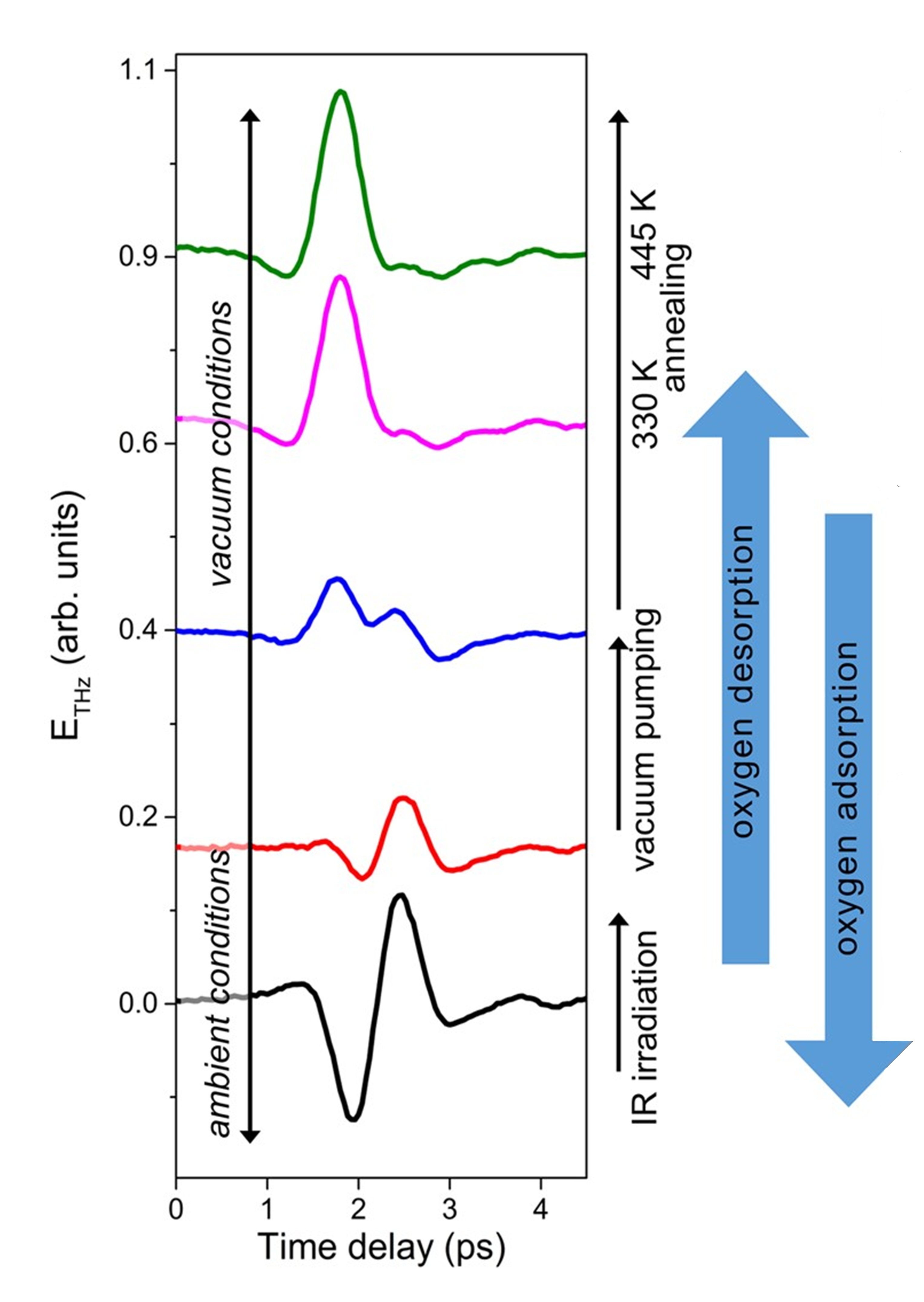
In the experiments conducted in [95] and [100], a monolayer of graphene grown by CVD was placed on the surface of a crystal of indium phosphide (InP). InP is known for its ability to emit coherent THz radiation efficiently. Specifically, when InP is photoexcited by femtosecond infrared pulses from a Ti:Sapphire laser, THz waves are generated from its surface. When the InP surface is coated by graphene, the impact of molecular adsorption and desorption on graphene can be probed through variations in the THz emission waveform under different conditions.
Figure 4 shows that, under atmospheric conditions and ambient temperature, the generated THz waveform exhibits a dip at 2 ps and a peak at 2.5 ps. However, after the graphene-coated InP was subjected to vacuum pumping and/or continuous femtosecond infrared irradiation, which desorbs O2, both peaks disappeared progressively, and a new positive peak replaced the dip at 2 ps. Further, when additional O2 adsorbates were eliminated through annealing, along with any remaining water present at the junction of graphene and InP, the THz waveforms of graphene-coated InP and uncoated InP converged. Nevertheless, when the sample was left in the air for several hours without femtosecond laser excitation, O2 molecules were re-adsorbed, leading to the recovery of the initial shape of the THz waveform. The original shape can also be restored by applying ultraviolet illumination to the sample, as it induces the oxidation of graphene [101, 102, 103]. All these results imply that the variations in the emitted THz radiation waveform result from the adsorption and desorption of O2 molecules on graphene.
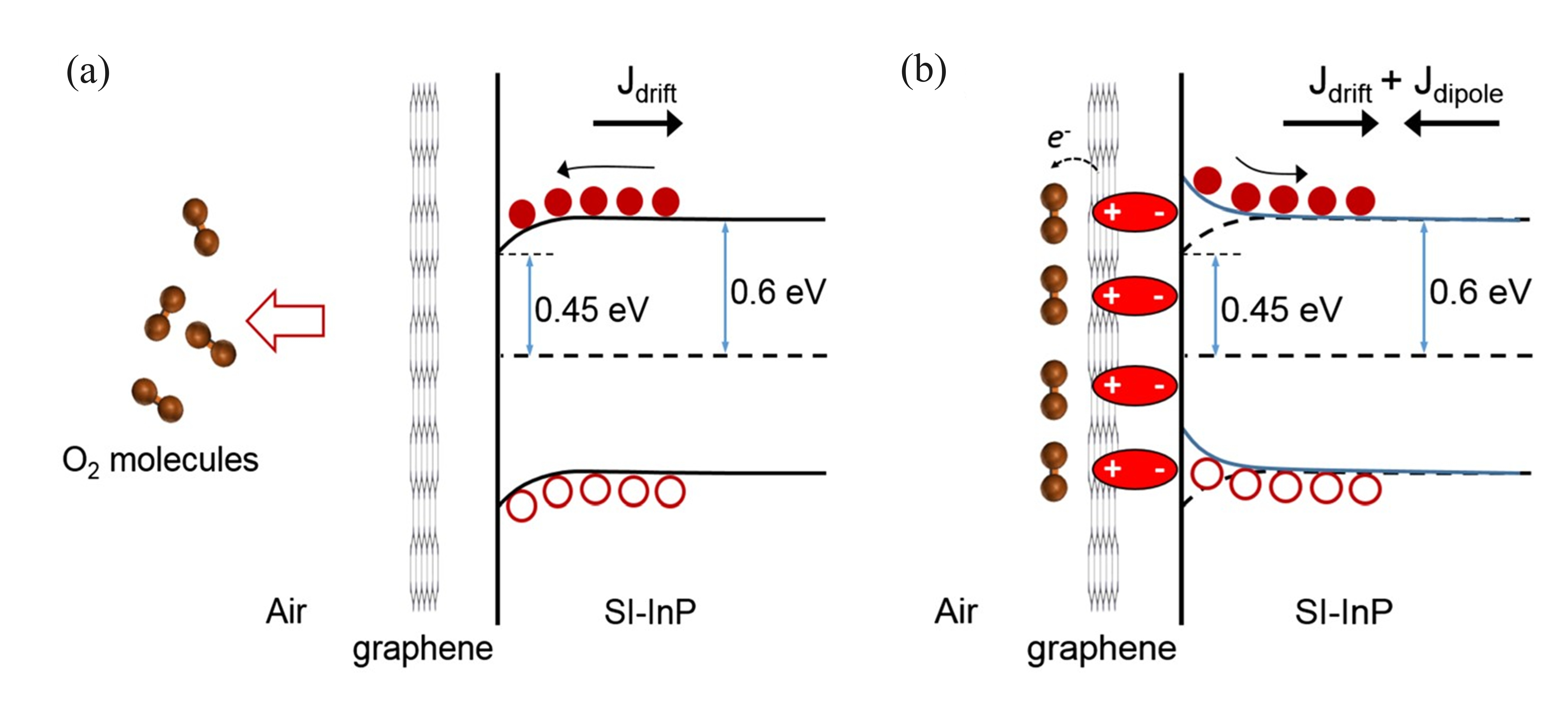
The effects of adsorption and desorption of O2 molecules on the THz waveform discussed above can be understood by explaining the origin of the THz radiation from InP. The THz wave generation in semiconductors can happen through either nonlinear or linear processes [105]. In this study, the laser induced low-intensity excitation, resulting in THz radiation primarily originating from linear processes described by the current surge model applied to the semiconductor surface. The electric field magnitude, , of the THz radiation is directly proportional to the time derivative of the transient current,
| (1) |
as articulated in [95, 100, 106, 107]. Upon photoexcitation of the sample, the current is generated through two mechanisms: the acceleration of photoexcited carriers by the surface depletion field resulting from the laser excitation (drift current), and the photo-Dember effect caused by the difference in the diffusion velocities of electrons and holes (diffusion current) [99, 108]. Given that InP is a semiconductor with a wide band gap ( eV), the contribution of the photo-Dember effect can be neglected. Therefore, the increase in current is primarily attributed to the transient photocarriers [105, 104]. The semi-insulating InP has a bulk Fermi level situated 0.6 eV below the conduction band, whereas the surface Fermi level is fixed at 0.45 eV below the conduction band [106, 104]. Consequently, the band curves down toward the surface, resulting in the drift current flowing in the opposite direction, toward the bulk of the InP substrate, as illustrated in Figure 5(a) in the absence of O2 molecules. On the contrary, when the sample is in contact with air, a transfer of electrons from graphene to O2 adsorbates occurs [100, 109, 110], resulting in the formation of localized electric dipoles at the surface of InP, and the subsequent creation of an electric field. This electric field induces an upward bending of the InP band, leading to an additional current denoted as , which is in the opposite direction of the initial current [111]; see Figure 5(b). This alteration diminishes the amplitude of the emitted THz radiation from the sample. When there is a high concentration of O2 adsorbates, contributes more than to the net surge current (), which flows toward the surface in this case [100, 104]. This process explains the variation in polarity of the THz waveform seen in Figure 4.
3.2 Biomolecular and Biochemical Sensing with Graphene
Information on the collective vibrational modes of biomolecules exists in the THz frequency range, and thus, THz spectroscopy is commonly used for chemical and biological sensing [113]. The mismatch between the wavelengths of THz radiation and the dimensions of the target molecules limit the sensitivity of THz spectroscopy in detecting small amounts of analytes. To enhance the interaction between THz waves and analytes, and amplify the signal, metamaterials can be utilized. Metamaterials have proven to be easy to use in both reflection and transmission modes, making them valuable in the field of biosensors [114, 115]. As the sensing device needs to be attached to a biointerface, flexibility is essential. However, the current processes for fabricating flexible metamaterials are expensive. Another issue is that the metamaterial structure introduces a gap separating the sensor and the target surfaces, diminishing the area of effective contact between the two and consequently reducing the sensing performance [112]. Hence, exploring methods to improve sensitivity without relying on metamaterials is underway, and cost-effective and sensitive metamaterial-free graphene-based THz molecular sensors have been proven promising.
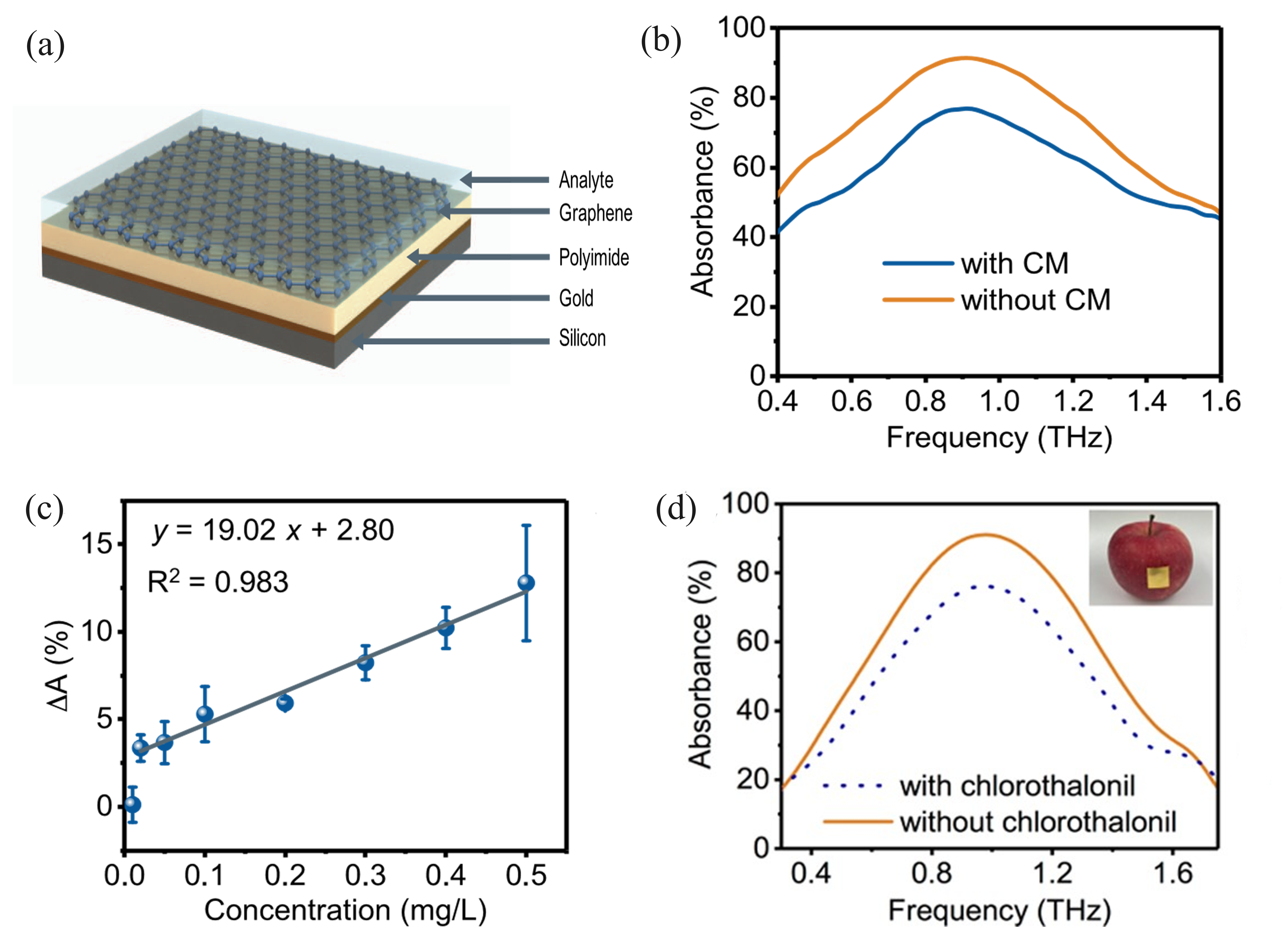
As described in Section 2.3, enhancing THz absorption of graphene can be achieved by utilizing TIR. Nevertheless, a promising approach involves a coherent-absorption-based trilayer structure. This structure consists of a layer of graphene and a metallic plate that are separated by a dielectric film, with the analyte of interest for investigation placed on top, as illustrated in Figure 6(a). The dielectric material used is a polyimide film, and the metal layer is a gold back-reflector that redirects unabsorbed THz radiation back to the graphene sheet, preventing it from leaving the graphene sensor. This trilayer structure serves as a horizontal waveguide and confines the impinging light. Enhanced absorption occurs when the incident and the reflected waves are in phase as they reach the graphene layer [112]. Moreover, owing to the metallic nature of graphene, the structure satisfies the impedance matching requirement, ensuring alignment between the impedance of free space and that of graphene [116].
To examine the sensing capability of the graphene sensor, chlorpyrifos methyl (CM), a widely used pesticide [117], can be used as an example of a biomolecule to detect. In Figure 6(b), THz absorption spectra are shown both in the absence and presence of CM molecules at a concentration of 0.5 mg/L. Initially, the absorption intensity is 91%, but it decreases to 78% with the introduction of CM molecules. This decrease is attributed to molecular adsorption, where the electrons of CM molecules encounter stacking interactions with graphene [94, 118]. These interactions cause the Fermi level to move toward the Dirac point of graphene, leading to a reduction in carrier density [112, 119]. The altered Fermi level increases the impedance mismatch between free space and the THz graphene sensor, resulting in a decrease in the absorption peak [120]. In Figure 6(c), the absorbance is presented as a function of CM concentration (0.02 to 0.50 mg/L), which shows good linearity with a coefficient of determination . The limit of detection (LOD) is determined to be 0.13 mg/L [112], which is better than the LOD obtained using metamaterials alone (0.204 mg/L) [121].
Furthermore, the fabrication of a flexible graphene sensor suitable for utilization at biointerfaces for pesticide sensing can be readily achieved by using electrically conductive tape as the metal layer in the trilayer structure. The resulting flexible graphene sensor can adhere to a curved surface without any gaps. For instance, when detecting chlorothalonil molecules on an apple surface at a concentration of 0.60 mg/L [Figure 6(d)], a reduction in the absorption peak is detected in the presence of chlorothalonil, similar to the previous case. This demonstrates the efficacy of this flexible graphene-based THz sensor in detecting pesticides at a biointerface [112].
Innovative approaches to enhance adsorption detection sensitivity involve metamaterial structures, such as nanoslots with tuned dimensions for resonance. Patterning of graphene either before or after metamaterial assembling has been explored. Mediated graphene nanoslot assemblies have demonstrated amplified sensitivities for detecting various single-stranded DNA species at the nanomole level, while patterned graphene nanoantennas enhanced sensitivity for lactose detection, resembling the structure discussed in Section 4.2 [122, 123]. Additionally, a CASR-Graphene metasurface microfluidic cell has been developed for label-free detection of 100 nM DNA, including the foodborne pathogen Escherichia coli [124]. Another study highlights virus detection capabilities through polarization-state sensing using a graphene chiral metasurface [125].
4 Gated Graphene for THz Device Development
Integrating gated graphene into THz devices enables manipulation of its electronic characteristics and achieves high-speed optical modulations for THz communications and imaging [126, 127, 128, 129, 130, 131, 132, 133, 134]. Beyond wave modulations, the control of plasmonic waves in graphene through gate voltage presents an innovative approach that could have significant implications for the progress of graphene plasmonic systems for a variety of applications [17, 5, 135, 136].
4.1 THz Wave Modulation
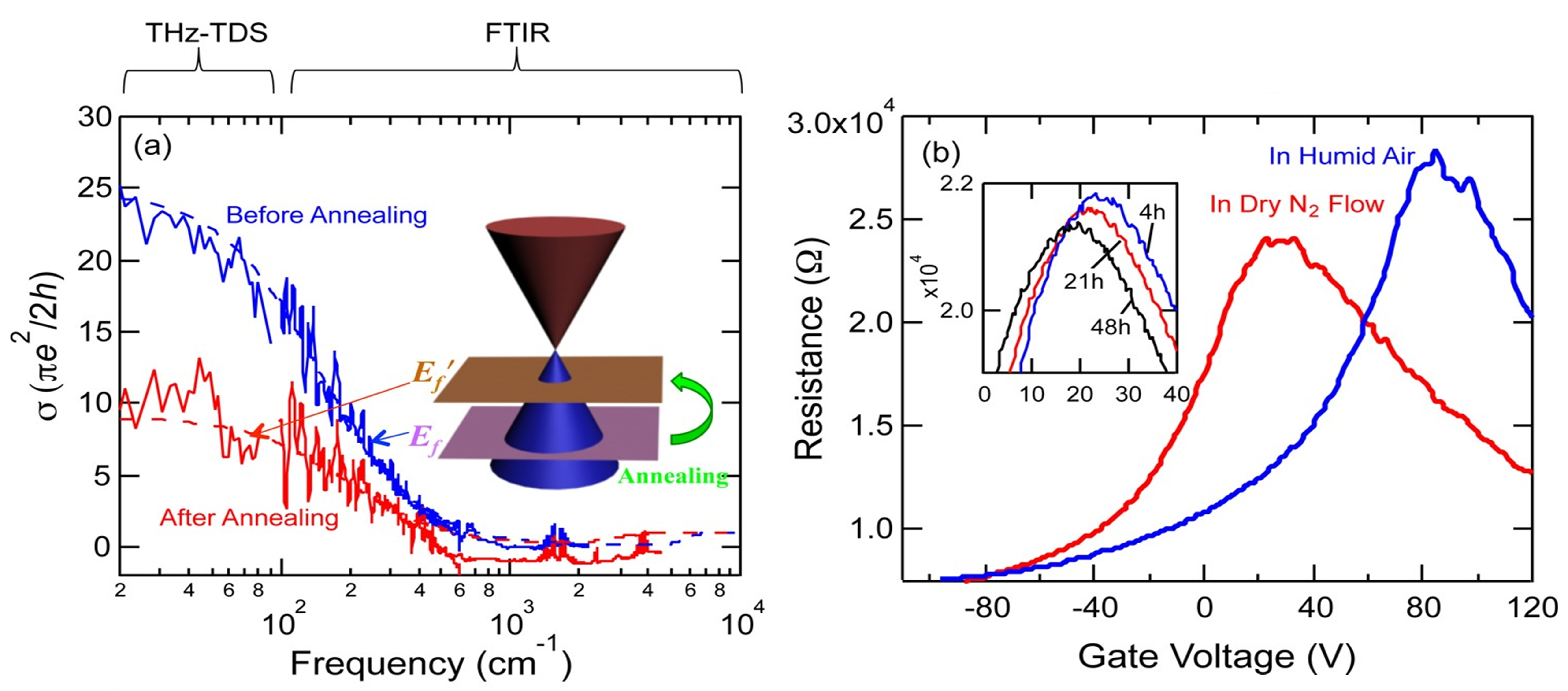
As introduced in Section 2.1, tuning the Fermi energy of graphene by using a gate voltage can influence THz transmission. The of a similar sample can also be tuned by inducing a conductivity change with thermal annealing [137, 138, 139] and can be monitored through THz-TDS combined with FTIR at higher frequencies [77]. Figure 7(a) shows that the Drude-like intraband conductivity (in units of , representing interband optical conductivity [140]) decreases after annealing (red solid line). This change is accompanied by a shift of the approaching the Dirac point. Figure 7(b) shows results for a gated graphene sample. In the presence of air, the Dirac point voltage is measured at 80 V. After placing the sample in an enclosed chamber with a continuous flow of dry N2 for one hour, the Dirac point voltage shifted to 30 V. On the other hand, when continuously pumped while inside a vacuum chamber, the progressively approached the Dirac point [141, 142]. After two days of vacuum pumping, the voltage at the Dirac point became smaller than 20 V [77], as illustrated in the inset of Figure 7(b).
Graphene-based THz modulators tend to display limited on/off ratios due to the single-layer thickness of graphene and the absence of resonance in intraband absorption within the THz region [143]. Enhancement of the extinction ratio and THz absorption of the graphene-engineered modulator can be achieved by using subwavelength apertures in a conductive medium that exhibit the extraordinary optical transmission (EOT) effect [144, 145, 146, 147, 148]. Ring-shaped apertures are particularly effective due to their strong polarization-insensitive EOT effect [149, 150, 151]. EOT describes a phenomenon in which a structure featuring subwavelength apertures in a metallic film enables greater light transmission than what is anticipated by ray optics. This occurs due to an enhancement of the electric field inside and near the apertures.
In the study described in [143], the structure of the graphene-assembled modulator comprised an EOT resonator consisting of a patterned lattice of ring apertures that operate in the THz range. The resonator was sandwiched on a -doped graphene layer, which is placed above the dielectric SiO2 substrate [152]; see Figures 8(a) and (b). To modulate the carrier density, a gate voltage was applied between the lower silicon substrate and the upper EOT structure. The ring aperture was subjected to a normally incident THz wave with linear polarization that induced a bright dipole mode. The radial electric-field element of the mode experienced a 2 variation in its phase along the ring contour, leading to a resonant EOT effect. This resonance occurred at frequency , where is the ring radius and is the effective index of the mode. The monolayer graphene absorption increased due to near-field enhancement resulting from EOT. The absorption enhancement factor was expressed as the ratio of absorption in the presence of the EOT structure to absorption in its absence. It was shown to be proportional to the monolayer graphene near-field intensity [143].
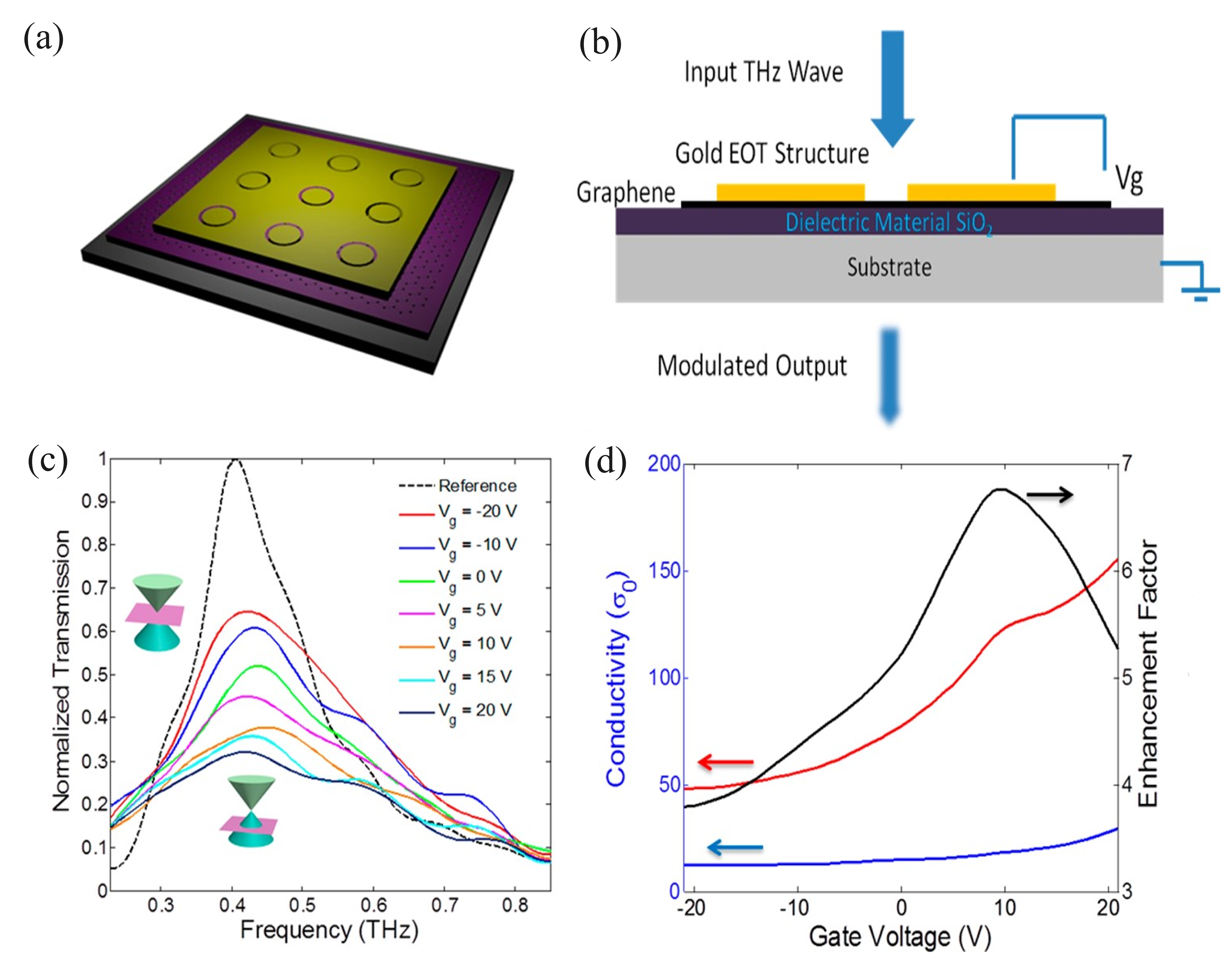
Transmission spectra for the THz modulator based on EOT graphene were normalized using the reference transmission spectrum corresponding to the EOT structure without graphene. The transmission spectra were obtained through THz-TDS while varying within the range of 20 to 20 V. They showed insensitivity to polarization, in accordance with the structural symmetry. In Figure 8(c), the central frequency showed minimal change across different gate voltages, whereas the transmission peak changed in response to the gate voltage. The variation in transmission is a consequence of the change in carrier concentration within graphene, which occurs due to the shift in induced by [77].
In Figure 8(d), the real part of the conductivity (in units of ) and the enhancement factor are displayed as a function of . At the resonance frequency, the EOT structure exhibits a conductivity (red line) approximately seven times greater than that observed in the absence of the structure (blue line). The primary contributor to this improvement is the robust near-field enhancement around the ring apertures, amplifying the interaction between the THz field and the monolayer graphene [143]. The breakdown of the SiO2 layer limits the gate voltage to a maximum reverse bias voltage of 20 V, which is when the THz absorption of graphene reaches a nonzero value, as indicated by the red line in Figure 8(d). This suggests that even when gets closer to the Dirac point, graphene will continue to exhibit a measurable THz conductivity, which is ascribed to the nonuniformity in across extensive areas of graphene [153]. Therefore, residual THz loss is induced by the presence of residual carriers in the film, as the Dirac point cannot be attained by the entire area under the same applied voltage [77, 143].
Recent advancements in gate-tuned graphene meta-devices have expanded the landscape of THz wave manipulation. Dynamic control of THz wavefronts has been achieved using gated ion gel and graphene metadevices [130]. Graphene metasurfaces have also been used to modulate the amplitude of refracted THz waves [131], and tunable phase [132]. Low-bias THz amplitude modulation has also been accomplished using a graphene and split-ring resonator metasurface [134]. A graphene/quartz modulator demonstrated a further ability to tune the Brewster angle [133]. These recent studies highlight the ongoing progress in graphene-based THz modulation technologies.
4.2 Surface Plasmon Polariton Manipulation
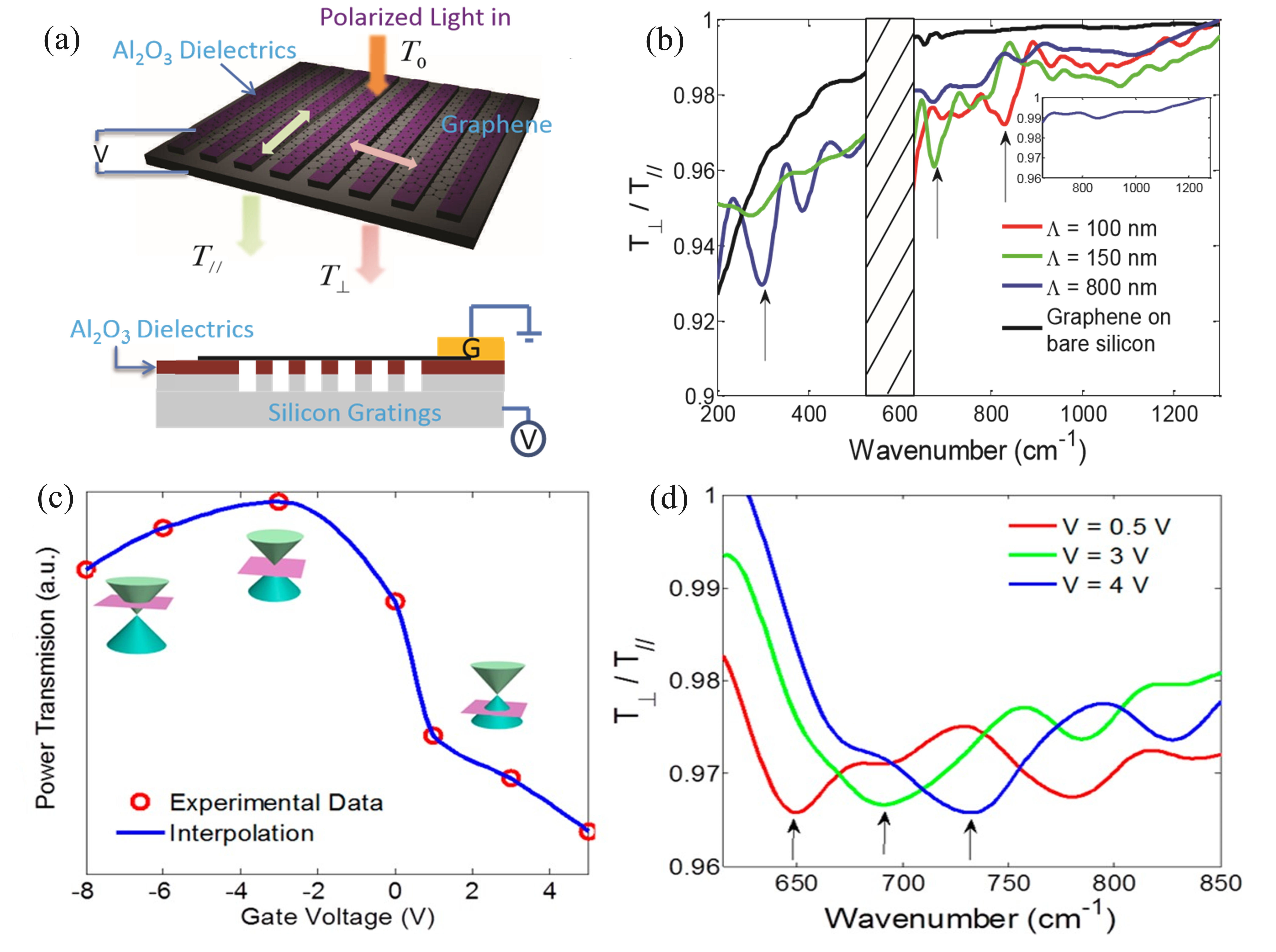
Acquiring control over the excitation and gate modulation of confined surface plasmon polaritons (SPPs) propagating through graphene can lead to various schemes for THz wave manipulation. However, the large difference in wavevector between the incident electromagnetic wave and the resulting excited SPPs in graphene presents a challenge. To overcome this issue, gratings can be employed to compensate for the wavevector mismatch. An example of such a grating involves using a silicon grating positioned beneath graphene with grating lines oriented perpendicular to the direction of the electric field in the incident wave. The silicon grating not only excites SPPs through guided-wave resonance but also acts as a gate electrode for modulating the carrier density in graphene, allowing a wide variation in resonance frequency [155, 154].
During the excitation of SPPs in graphene by the incident wave, a dissipation of the optical energy occurs via an ohmic loss [76, 156], which leads to a dip in the amplitude of the transmitted wave at around the resonance frequency:
| (2) |
where and are the dielectric constants of the dielectric materials sandwiching the graphene film and represents the grating period [154, 157, 158]. As displayed in Figure 9(a), the structure is composed of periodically spaced trenches, etched in a lightly doped silicon substrate. The dielectric layer used is aluminum oxide (Al2O3), which is placed onto the grating. Following this, a monolayer of graphene, grown through CVD, is transferred on top of the grating [76, 154].
The phase-matching effect is observed when SPPs propagate perpendicular to the grating lines. Consequently, SPPs are only excited when the incident light and grating lines are cross-polarized. This leads to a dip in the transmission spectrum (), with no resonance features in the co-polarized configuration (). Figure 9(b) shows the ratio as a function of frequency for different grating periods, which reveals a resonant notch when incident light with the appropriate polarization interacts with the graphene SPPs. There is no discernible variation in transmission between parallel and perpendicular polarized beams when graphene is on a bare silicon wafer. In contrast, the three other devices with gratings display a dip in light transmission at specific frequencies when the incident wave is polarized perpendicular to the lines of the grating, emphasizing the important role of gratings in the SPP excitation [154].
With an applied voltage, the Al2O3 layer underneath the graphene monolayer serves as a back-gate structure to electrically modulate the carrier concentration, and consequently, the resonance frequency. Through THz-TDS measurements, Figure 9(c) illustrates the transmitted power of THz radiation as a function of , indicating the effective carrier density change in the monolayer of graphene from the -doped to the -doped region. Figure 9(d) depicts the electrical modulation of plasmon resonance by plotting as a function of frequency under various within the midinfrared region. A substantial blue shift in resonance frequency becomes evident upon increasing from 0.5 to 4 V.
Several reports have explored novel avenues in graphene-based plasmonic technologies. Current-driven THz emission from graphene plasmonic oscillators [159] has introduced dynamic control possibilities for THz radiation. Studies on multilayer graphene THz plasmonic structures for enhanced frequency tuning [160] and resonant THz detection using graphene plasmons [161] have contributed to expanding the capabilities of efficient THz modulation and detection with graphene.
5 Conclusions and Prospects
In this review, we summarized some distinctive characteristics of graphene and explored their benefits for applications in THz technology. The modulation of THz transmission has been successfully achieved by tuning the Fermi level by manipulating the carrier density with an external gate voltage. Parallel-plate waveguides have proven effective in modulating transmitted THz waves, exhibiting better sensitivity than traditional THz spectroscopy. The phenomenon of total internal reflection in a unique waveguide structure has revealed that the presence of graphene results in enhanced absorption, particularly with -polarized THz waves. Furthermore, studying the adsorption and desorption of O2 molecules on graphene under different conditions has helped explain the variations in emitted THz waves. This interaction between external molecules and graphene has enabled the development of flexible graphene devices capable of detecting molecules like pesticides on a biointerface without needing metamaterials. In addition to the gate voltage application, thermal annealing has proven to be an effective method for shifting the Fermi level. The use of metallic ring apertures has demonstrated the enhancement of THz absorption in graphene through the extraordinary optical transmission phenomenon. Moreover, optical gratings have been employed to excite propagating surface plasmon polaritons in graphene, creating opportunities to develop active plasmonic devices.
Due to the unique combination of properties of graphene, many technological limitations present in conventional devices operating in the THz frequency range can be overcome. All of the characteristics of graphene make it suitable for a wide range of applications, including optical communication systems, biomolecule sensing, and plasmonics research. Hence, there is a considerable opportunity for further research studies in this field.
Acknowledgements
J.D. and J.K. acknowledge support from the Robert A. Welch Foundation through Grant No. C-1509, the Air Force Office of Scientific Research through Grant No. FA9550-22-1-0382, and the Chan Zuckerberg Initiative through Grant No. WU-21-357.
References
- [1] K. S. Novoselov, A. K. Geim, S. V. Morozov, D. Jiang, Y. Zhang, S. V. Dubonos, I. V. Grigorieva, A. A. Firsov, Science 2004, 306, 666.
- [2] A. K. Geim, K. S. Novoselov, Nat. Mater. 2007, 6, 183.
- [3] M. Poot, H. S. J. van der Zant, Appl. Phys. Lett. 2008, 92, 063111.
- [4] F. Bonaccorso, Z. Sun, T. Hasan, A. C. Ferrari, Nat. Photonics 2010, 4, 611.
- [5] Y. Li, K. Tantiwanichapan, A. K. Swan, R. Paiella, Nanophotonics 2020, 9, 1901.
- [6] S. Ghosh, I. Calizo, D. Teweldebrhan, E. P. Pokatilov, D. L. Nika, A. A. Balandin, W. Bao, F. Miao, C. N. Lau, Appl. Phys. Lett. 2008, 92, 151911.
- [7] A. K. Geim, Science 2009, 324, 1530.
- [8] C. Lee, X. Wei, J. W. Kysar, J. Hone, Science 2008, 321, 385.
- [9] A. H. Castro Neto, F. Guinea, N. M. R. Peres, K. S. Novoselov, A. K. Geim, Rev. Mod. Phys. 2009, 81, 109.
- [10] A. A. Balandin, Nat. Mater. 2011, 10, 569.
- [11] F. Schwierz, Nat. Nanotechnol. 2010, 5, 487.
- [12] Q. Bao, K. P. Loh, ACS Nano 2012, 6, 3677.
- [13] R. Raccichini, A. Varzi, S. Passerini, B. Scrosati, Nat. Mater. 2015, 14, 271.
- [14] C. Chung, Y.-K. Kim, D. Shin, S.-R. Ryoo, B. H. Hong, D.-H. Min, Acc. Chem. Res. 2013, 46, 2211.
- [15] R. R. Hartmann, J. Kono, M. E. Portnoi, Nanotechnology 2014, 25, 322001.
- [16] L. Yang, J. Deslippe, C.-H. Park, M. L. Cohen, S. G. Louie, Phys. Rev. Lett. 2009, 103, 186802.
- [17] A. N. Grigorenko, M. Polini, K. Novoselov, Nat. Photonics 2012, 6, 749.
- [18] J. J. Dean, H. M. van Driel, Appl. Phys. Lett. 2009, 95, 261910.
- [19] G. Soavi, G. Wang, H. Rostami, D. G. Purdie, D. De Fazio, T. Ma, B. Luo, J. Wang, A. K. Ott, D. Yoon, S. A. Bourelle, J. E. Muench, I. Goykhman, S. Dal Conte, M. Celebrano, A. Tomadin, M. Polini, G. Cerullo, A. C. Ferrari, Nat. Nanotechnol. 2018, 13, 583.
- [20] N. Yoshikawa, T. Tamaya, K. Tanaka, Science 2017, 356, 736.
- [21] D.-H. Chae, T. Utikal, S. Weisenburger, H. Giessen, K. V. Klitzing, M. Lippitz, J. Smet, Nano Lett. 2011, 11, 1379.
- [22] C.-J. Kim, A. Sánchez-Castillo, Z. Ziegler, Y. Ogawa, C. Noguez, J. Park, Nat. Nanotechnol. 2016, 11, 520.
- [23] R. R. Nair, P. Blake, A. N. Grigorenko, K. S. Novoselov, T. J. Booth, T. Stauber, N. M. R. Peres, A. K. Geim, Science 2008, 320, 1308.
- [24] P. A. Obraztsov, P. A. Chizhov, T. Kaplas, V. V. Bukin, M. Silvennoinen, C.-F. Hsieh, K. Konishi, N. Nemoto, M. Kuwata-Gonokami, ACS Photonics 2019, 6, 1780.
- [25] Q. Zhou, Q. Qiu, Z. Huang, Opt. Laser Technol. 2023, 157, 108558.
- [26] J. Liu, X. Li, R. Jiang, K. Yang, J. Zhao, S. A. Khan, J. He, P. Liu, J. Zhu, B. Zeng, Sensors 2021, 21, 4987.
- [27] J. Neu, C. A. Schmuttenmaer, J. Appl. Phys. 2018, 124, 1231101.
- [28] R. A. Lewis, J. Phys. D: Appl. Phys. 2019, 52, 433001.
- [29] A. Y. Pawar, D. D. Sonawane, K. B. Erande, D. V. Derle, Drug Invent. Today 2013, 5, 157.
- [30] D. M. Mittleman, Opt. Express 2018, 26, 9417.
- [31] K. F. Mak, M. Y. Sfeir, Y. Wu, C. H. Lui, J. A. Misewich, T. F. Heinz, Phys. Rev. Lett. 2008, 101, 196405.
- [32] J. Wang, X. Hu, J. Nanotechnol. 2016, 2016, 1.
- [33] M. T. Mihnev, F. Kadi, C. J. Divin, T. Winzer, S. Lee, C.-H. Liu, Z. Zhong, C. Berger, W. A. De Heer, E. Malic, A. Knorr, T. B. Norris, Nat. Commun. 2016, 7, 11617.
- [34] H. Choi, F. Borondics, D. A. Siegel, S. Y. Zhou, M. C. Martin, A. Lanzara, R. A. Kaindl, Appl. Phys. Lett. 2009, 94, 172102.
- [35] L. Ren, Q. Zhang, S. Nanot, I. Kawayama, M. Tonouchi, J. Kono, J. Infrared Millim. Terahertz Waves 2012, 33, 846.
- [36] A. Tomadin, S. M. Hornett, H. I. Wang, E. M. Alexeev, A. Candini, C. Coletti, D. Turchinovich, M. Kläui, M. Bonn, F. H. L. Koppens, E. Hendry, M. Polini, K.-J. Tielrooij, Sci. Adv. 2018, 4, eaar5313.
- [37] B. Sensale-Rodriguez, R. Yan, M. M. Kelly, T. Fang, K. Tahy, W. S. Hwang, D. Jena, L. Liu, H. G. Xing, Nat. Commun. 2012, 3, 780.
- [38] L. Wang, N. An, X. He, X. Zhang, A. Zhu, B. Yao, Y. Zhang, Nanomaterials 2022, 12, 2097.
- [39] J. Park, Y. H. Ahn, C. Ruiz-Vargas, Nano Lett. 2009, 9, 1742.
- [40] K. Kang, D. Abdula, D. G. Cahill, M. Shim, Phys. Rev. B 2010, 81, 165405.
- [41] M. Breusing, S. Kuehn, T. Winzer, E. Malić, F. Milde, N. Severin, J. P. Rabe, C. Ropers, A. Knorr, T. Elsaesser, Phys. Rev. B 2011, 83, 153410.
- [42] D. Sun, Z.-K. Wu, C. Divin, X. Li, C. Berger, W. A. De Heer, P. N. First, T. B. Norris, Phys. Rev. Lett. 2008, 101, 157402.
- [43] R. W. Newson, J. Dean, B. Schmidt, H. M. Van Driel, Opt. Express 2009, 17, 2326.
- [44] B. A. Ruzicka, S. Wang, J. Liu, K.-P. Loh, J. Z. Wu, H. Zhao, Opt. Mater. Express 2012, 2, 708.
- [45] K.-C. Lin, M.-Y. Li, L. J. Li, D. C. Ling, C. C. Chi, J.-C. Chen, J. Appl. Phys. 2013, 113, 133511.
- [46] H. Wang, J. H. Strait, P. A. George, S. Shivaraman, V. B. Shields, M. Chandrashekhar, J. Hwang, F. Rana, M. G. Spencer, C. S. Ruiz-Vargas, J. Park, Appl. Phys. Lett. 2010, 96, 081917.
- [47] D. Golla, A. Brasington, B. J. LeRoy, A. Sandhu, APL Mater. 2017, 5, 056101.
- [48] L. M. Malard, K. Fai Mak, A. H. Castro Neto, N. M. R. Peres, T. F. Heinz, New J. Phys. 2013, 15, 015009.
- [49] R. Gatamov, A. Baydin, H. Krzyzanowska, N. Tolk, Mater. Res. Express 2020, 7, 095601.
- [50] S. Scarfe, W. Cui, A. Luican-Mayer, J.-M. Ménard, Sci. Rep. 2021, 11, 8729.
- [51] J. M. Dawlaty, S. Shivaraman, M. Chandrashekhar, F. Rana, M. G. Spencer, Appl. Phys. Lett. 2008, 92, 042116.
- [52] P. A. George, J. Strait, J. Dawlaty, S. Shivaraman, M. Chandrashekhar, F. Rana, M. G. Spencer, Nano Lett. 2008, 8, 4248.
- [53] J. Shang, Z. Luo, C. Cong, J. Lin, T. Yu, G. G. Gurzadyan, Appl. Phys. Lett. 2010, 97, 163103.
- [54] B. A. Ruzicka, L. K. Werake, H. Zhao, S. Wang, K. P. Loh, Appl. Phys. Lett. 2010, 96, 173106.
- [55] L. Huang, G. V. Hartland, L.-Q. Chu, Luxmi, R. M. Feenstra, C. Lian, K. Tahy, H. Xing, Nano Lett. 2010, 10, 1308.
- [56] J. Shang, T. Yu, J. Lin, G. G. Gurzadyan, ACS Nano 2011, 5, 3278.
- [57] L. Huang, B. Gao, G. Hartland, M. Kelly, H. Xing, Surf. Sci. 2011, 605, 1657.
- [58] X. Zhao, Z.-B. Liu, W.-B. Yan, Y. Wu, X.-L. Zhang, Y. Chen, J.-G. Tian, Appl. Phys. Lett. 2011, 98, 121905.
- [59] S. Tani, F. Blanchard, K. Tanaka, Phys. Rev. Lett. 2012, 109, 166603.
- [60] K. Chen, H. Li, L.-P. Ma, W. Ren, T.-F. Chung, H.-M. Cheng, Y. P. Chen, T. Lai, Carbon 2014, 72, 402.
- [61] F. Kadi, T. Winzer, E. Malic, A. Knorr, F. Göttfert, M. Mittendorff, S. Winnerl, M. Helm, Phys. Rev. Lett. 2014, 113, 035502.
- [62] K. Chen, M. N. Yogeesh, Y. Huang, S. Zhang, F. He, X. Meng, S. Fang, N. Sheehan, T. H. Tao, S. R. Bank, J.-F. Lin, D. Akinwande, P. Sutter, T. Lai, Y. Wang, Carbon 2016, 107, 233.
- [63] M. Guo, L.-P. Ma, W. Ren, T. Lai, Photonics Res. 2020, 8, 17.
- [64] V. Pistore, O. Balci, J. Zhang, S. M. Schinde, A. Meersha, A. C. Ferrari, M. S. Vitiello, 2D Mater. 2022, 9, 025018.
- [65] T.-P. Nguyen, M. Klymenko, G. Beane, M. Oldfield, K. Xing, M. Gebert, S. Bhattacharyya, M. S. Fuhrer, J. H. Cole, A. Schiffrin, arXiv 2023, cond-mat.mtrl-sci, 2310.06180.
- [66] J. Lu, H. Liu, Opt. Commun. 2018, 406, 24.
- [67] I. Ivanov, M. Bonn, Z. Mics, D. Turchinovich, EPL 2015, 111, 67001.
- [68] C. J. Docherty, M. B. Johnston, J. Infrared Millim. Terahertz Waves 2012, 33, 797.
- [69] G. Jnawali, Y. Rao, H. Yan, T. F. Heinz, Nano Lett. 2013, 13, 524.
- [70] A. J. Frenzel, C. H. Lui, W. Fang, N. L. Nair, P. K. Herring, P. Jarillo-Herrero, J. Kong, N. Gedik, Appl. Phys. Lett. 2013, 102, 113111.
- [71] E. Cinquanta, E. A. A. Pogna, L. Gatto, S. Stagira, C. Vozzi, Adv. Phys. X 2023, 8, 2120416.
- [72] P. Han, X. Wang, Y. Zhang, Adv. Opt. Mater. 2020, 8, 1900533.
- [73] J. Horng, C.-F. Chen, B. Geng, C. Girit, Y. Zhang, Z. Hao, H. A. Bechtel, M. Martin, A. Zettl, M. F. Crommie, Y. R. Shen, F. Wang, Phys. Rev. B 2011, 83, 165113.
- [74] H. Lee, K. Paeng, I. S. Kim, Synth. Met. 2018, 244, 36.
- [75] J. H. Gosling, O. Makarovsky, F. Wang, N. D. Cottam, M. T. Greenaway, A. Patanè, R. D. Wildman, C. J. Tuck, L. Turyanska, T. M. Fromhold, Commun. Phys. 2021, 4, 30.
- [76] W. Gao, Q. Zhang, L. Ren, Z. Jin, J. H. Kim, J. Kono, SPIE 2014, 8984, 61.
- [77] L. Ren, Q. Zhang, J. Yao, Z. Sun, R. Kaneko, Z. Yan, S. Nanot, Z. Jin, I. Kawayama, M. Tonouchi, J. M. Tour, J. Kono, Nano Lett. 2012, 12, 3711.
- [78] M. Razanoelina, F. R. Bagsican, I. Kawayama, X. Zhang, L. Ma, H. Murakami, R. Vajtai, P. M. Ajayan, J. Kono, M. Tonouchi, Opt. Express 2016, 24, 3885.
- [79] M. Razanoelina, R. Kinjo, K. Takayama, I. Kawayama, H. Murakami, D. M. Mittleman, M. Tonouchi, J. Infrared Millim. Terahertz Waves 2015, 36, 1182.
- [80] J. Wu, X. Chen, K. Wang, X. Zhang, Y. Li, H. Wang, J. Han, Infrared Phys. Technol. 2021, 118, 103875.
- [81] M. Naftaly, R. Dudley, Opt. Lett. 2009, 34, 1213.
- [82] Q. Sun, X. Chen, X. Liu, R. I. Stantchev, E. Pickwell‐MacPherson, Adv. Opt. Mater. 2020, 8, 1900535.
- [83] M. S. Ukhtary, E. H. Hasdeo, A. R. T. Nugraha, R. Saito, Appl. Phys. Express 2015, 8, 055102.
- [84] Y. Harada, M. S. Ukhtary, M. Wang, S. K. Srinivasan, E. H. Hasdeo, A. R. T. Nugraha, G. T. Noe, Y. Sakai, R. Vajtai, P. M. Ajayan, R. Saito, J. Kono, ACS Photonics 2017, 4, 121.
- [85] X. Liu, Z. Chen, E. P. J. Parrott, B. S.-Y. Ung, J. Xu, E. Pickwell‐MacPherson, Adv. Opt. Mater. 2017, 5, 1600697.
- [86] Y. Sun, R. Degl’Innocenti, D. A. Ritchie, H. E. Beere, L. Xiao, M. Ruggiero, J. A. Zeitler, R. I. Stantchev, D. Chen, Z. Peng, E. MacPherson, X. Liu, Photonics Res. 2018, 6, 1151.
- [87] F. D’Angelo, Z. Mics, M. Bonn, D. Turchinovich, Opt. Express 2014, 22, 12475.
- [88] M. Rahmanshahi, S. N. Kourani, S. Golmohammadi, H. Baghban, H. Vahed, Plasmonics 2021, 16, 1665.
- [89] L. Ye, F. Zeng, Y. Zhang, Q. H. Liu, Carbon 2019, 148, 317.
- [90] W. Nsengiyumva, S. Zhong, L. Zheng, W. Liang, B. Wang, Y. Huang, X. Chen, Y. Shen, IEEE Trans. Instrum. Meas. 2023, 72, 1.
- [91] L. Wei, L. Yu, H. Jiaoqi, H. Guorong, Z. Yang, F. Weiling, Front. Lab. Med. 2018, 2, 127.
- [92] N. L. Rangel, J. M. Seminario, J. Phys. Chem. A 2008, 112, 13699.
- [93] D.-K. Lee, J.-H. Kang, J. Kwon, J.-S. Lee, S. Lee, D. H. Woo, J. H. Kim, C.-S. Song, Q.-H. Park, M. Seo, Sci. Rep. 2017, 7, 8146.
- [94] W. Xu, L. Xie, J. Zhu, L. Tang, R. Singh, C. Wang, Y. Ma, H.-T. Chen, Y. Ying, Carbon 2019, 141, 247.
- [95] F. R. Bagsican, A. Winchester, X. Z. S. Ghosh, L. Ma, M. Wang, H. Murakami, S. Talapatra, R. Vajtai, P. M. Ajayan, J. Kono, M. Tonouchi, I. Kawayama, Sci. Rep. 2017, 7, 1774.
- [96] I. Santoso, R. S. Singh, P. K. Gogoi, T. C. Asmara, D. Wei, W. Chen, A. T. S. Wee, V. M. Pereira, A. Rusydi, Phys. Rev. B 2014, 89, 075134.
- [97] H.-C. Chang, Y.-J. Huang, H.-Y. Chang, W.-J. Su, Y.-T. Shih, Y.-S. Huang, K.-Y. Lee, Appl. Phys. Express 2014, 7, 055101.
- [98] C. J. Docherty, C.-T. Lin, H. J. Joyce, R. J. Nicholas, L. M. Herz, L. J. Li, M. B. Johnston, Nat. Commun. 2012, 3, 1228.
- [99] Y. Huang, Z. Yao, C. He, L. Zhu, L. Zhang, J. Bai, X. Xu, J. Phys. Condens. Matter 2019, 31, 153001.
- [100] Y. Sano, I. Kawayama, M. Tabata, K. A. Salek, H. Murakami, M. Wang, R. Vajtai, P. M. Ajayan, J. Kono, M. Tonouchi, Sci Rep 2014, 4, 6046.
- [101] F. Gunes, G. Han, H.-J. Shin, S. Lee, M. Jin, L. D. Dinh, S. Chae, E. Kim, F. Yao, A. Benayad, J. H. Choi, Y. H. Lee, Nano 2011, 6, 409.
- [102] N. Mitoma, R. Nouchi, K. Tanigaki, J. Phys. Chem. C 2013, 117, 1453.
- [103] S. Zhao, S. Surwade, Z. Li, H. Liu, Nanotechnology 2012, 23, 355703.
- [104] F. R. Bagsican, X. Zhang, L. Ma, M. Wang, H. Murakami, R. Vajtai, P. M. Ajayan, J. Kono, M. Tonouchi, I. Kawayama, J. Infrared Millim. Terahertz Waves 2016, 37, 1117.
- [105] P. Gu, M. Tani, S. Kono, K. Sakai, X.-C. Zhang, J. Appl. Phys. 2002, 91, 5533.
- [106] M. Nakajima, M. Hangyo, M. Ohta, H. Miyazaki, Phys. Rev. B 2003, 67, 195308.
- [107] M. Nakajima, Y. Oda, T. Suemoto, Appl. Phys. Lett. 2004, 85, 2694.
- [108] M. Tonouchi, J. Appl. Phys. 2020, 127, 245703.
- [109] Y. Yang, R. Murali, Appl. Phys. Lett. 2011, 98, 093116.
- [110] P. L. Levesque, S. S. Sabri, C. M. Aguirre, J. Guillemette, M. Siaj, P. Desjardins, T. Szkopek, R. Martel, Nano Lett. 2011, 11, 132.
- [111] W. Du, Y. Huang, Y. Zhou, X. Xu, J. Phys. D: Appl. Phys. 2022, 55, 223002.
- [112] W. Xu, Y. Huang, R. Zhou, Q. Wang, J. Yin, J. Kono, J. Ping, L. Xie, Y. Ying, ACS Appl. Mater. Interfaces 2020, 12, 44281.
- [113] B. Ferguson, X.-C. Zhang, Nat. Mater. 2002, 1, 26.
- [114] K. V. Sreekanth, Y. Alapan, M. ElKabbash, E. Ilker, M. Hinczewski, U. A. Gurkan, A. D. Luca, G. Strangi, Nat. Mater. 2016, 15, 621.
- [115] M. Seo, H.-R. Park, Adv. Opt. Mater. 2020, 8, 1900662.
- [116] C. M. Watts, X. Liu, W. J. Padilla, Adv. Mater. 2012, 24, OP98.
- [117] W. Wei, X. Zong, X. Wang, L. Yin, Y. Pu, S. Liu, Food Chem. 2012, 135, 888.
- [118] W. Xu, Q. Wang, R. Zhou, S. Hameed, Y. Ma, L. Xie, Y. Ying, RSC Adv. 2022, 12, 28678.
- [119] Y. Guo, Y. Han, Y. Guo, C. Dong, Biosens. Bioelectron. 2013, 45, 95.
- [120] A. C. Tasolamprou, A. D. Koulouklidis, C. Daskalaki, C. P. Mavidis, G. Kenanakis, G. Deligeorgis, Z. Viskadourakis, P. Kuzhir, S. Tzortzakis, M. Kafesaki, E. N. Economou, C. M. Soukoulis, ACS Photonics 2019, 6, 720.
- [121] W. Xu, L. Xie, J. Zhu, W. Wang, Z. Ye, Y. Ma, C.-Y. Tsai, S. Chen, Y. Ying, Food Chem. 2017, 218, 330.
- [122] S.-H. Lee, J.-H. Choe, C. Kim, S. Bae, J.-S. Kim, Q.-H. Park, M. Seo, Sens. Actuators B Chem. 2020, 310, 127841.
- [123] G. Choi, S. J. Hong, Y.-M. Bahk, Sci. Rep. 2019, 9, 9749.
- [124] R. Zhou, C. Wang, Y. Huang, K. Huang, Y. Wang, W. Xu, L. Xie, Y. Ying, Biosens. Bioelectron. 2021, 188, 113336.
- [125] M. Amin, O. Siddiqui, H. Abutarboush, M. Farhat, R. Ramzan, Carbon 2021, 176, 580.
- [126] M. Hasan, S. Arezoomandan, H. Condori, B. Sensale-Rodriguez, Nano Commun. Netw. 2016, 10, 68.
- [127] M. Kim, S.-H. Kim, C. Kang, S. Kim, C.-S. Kee, Sci. Rep. 2023, 13, 6680.
- [128] A. M. Zaman, Y. Lu, X. Romain, N. W. Almond, O. J. Burton, J. Alexander-Webber, S. Hofmann, T. Mitchell, J. D. P. Griffiths, H. E. Beere, D. A. Ritchie, R. Degl’Innocenti, IEEE Trans. THz Sci. Technol. 2022, 12, 520.
- [129] Z. T. Ma, Z. X. Geng, Z. Y. Fan, J. Liu, H. D. Chen, Research 2019, 2019, 6482975.
- [130] Q. Li, X. Cai, T. Liu, M. Jia, Q. Wu, H. Zhou, H. Liu, Q. Wang, X. Ling, C. Chen, F. Ding, Q. He, Y. Zhang, S. Xiao, L. Zhou, Nanophotonics 2022, 11, 2085.
- [131] T.-T. Kim, H. Kim, M. Kenney, H. S. Park, H.-D. Kim, B. Min, S. Zhang, Adv. Opt. Mater. 2017, 6, 1700507.
- [132] Z. Miao, Q. Wu, X. Li, Q. He, K. Ding, Z. An, Y. Zhang, L. Zhou, Phys. Rev. X 2015, 5, 041027.
- [133] Z. Chen, X. Chen, L. Tao, K. Chen, M. Long, X. Liu, K. Yan, R. I. Stantchev, E. Pickwell-MacPherson, J.-B. Xu, Nat. Commun. 2018, 9, 4909.
- [134] R. Degl’Innocenti, D. S. Jessop, Y. D. Shah, J. Sibik, J. A. Zeitler, P. R. Kidambi, S. Hofmann, H. E. Beere, D. A. Ritchie, ACS Nano 2014, 8, 2548.
- [135] S. Huang, C. Song, G. Zhang, H. Yan, Nanophotonics 2016, 6, 1191.
- [136] R. Wang, X. Ren, Z. Yan, L. Jiang, W. E. I. Sha, G. Shan, Front. Phys. 2019, 14, 13603.
- [137] M. Chen, Y. Wang, J. Wen, H. Chen, W. Ma, F. Fan, Y. Huang, Z. Zhao, ACS Appl. Mater. Interfaces 2019, 11, 6411.
- [138] P. Kumar, M. Šilhavík, J. Červenka, P. Kužel, J. Phys. D: Appl. Phys. 2023, 56, 505103.
- [139] A. Nourbakhsh, M. Cantoro, A. Klekachev, F. Clemente, B. Sorée, M. H. van der Veen, T. Vosch, A. Stesmans, B. Sels, S. De Gendt, J. Phys. Chem. C 2010, 114, 6894.
- [140] G. L. Klimchitskaya, V. M. Mostepanenko, Phys. Rev. B 2016, 93, 245419.
- [141] M. Ishigami, J. H. Chen, W. G. Cullen, M. S. Fuhrer, E. D. Williams, Nano Lett. 2007, 7, 1643.
- [142] J. Moser, A. Verdaguer, D. Jimenez, A. Barreiro, A. Bachtold, Appl. Phys. Lett. 2008, 92, 123507.
- [143] W. Gao, J. Shu, K. Reichel, D. V. Nickel, X. He, G. Shi, R. Vajtai, P. M. Ajayan, J. Kono, D. M. Mittleman, Q. Xu, Nano Lett. 2014, 14, 1242.
- [144] H.-T. Chen, H. Lu, A. K. Azad, R. D. Averitt, A. C. Gossard, S. A. Trugman, J. F. O’Hara, A. J. Taylor, Opt. Express 2008, 16, 7641.
- [145] M. A. Seo, H. R. Park, S. M. Koo, D. J. Park, J. H. Kang, O. K. Suwal, S. S. Choi, P. C. M. Planken, G. S. Park, N. K. Park, Q. H. Park, D. S. Kim, Nat. Photonics 2009, 3, 152.
- [146] E. Hendry, M. J. Lockyear, J. G. Rivas, L. Kuipers, M. Bonn, Phys. Rev. B 2007, 75, 235305.
- [147] T. Cao, M. Lian, X. Chen, L. Mao, K. Liu, J. Jia, Y. Su, H. Ren, S. Zhang, Y. Xu, J. Chen, Z. Tian, D. Guo, OES 2021, 1, 210010.
- [148] Z. Gao, Y. Shi, M. Li, J. Song, X. Liu, X. Wang, F. Yang, ACS Omega 2021, 6, 29746.
- [149] J. Shu, C. Qiu, V. Astley, D. Nickel, D. M. Mittleman, Q. Xu, Opt. Express 2011, 19, 26666.
- [150] M. Fu, J. Wang, S. Guo, Z. Wang, P. Yang, Y. Niu, Nanomaterials 2022, 12, 3763.
- [151] W. Gao, C. Yu, R. Chen, Adv. Photon. Res. 2021, 2, 2100048.
- [152] J. W. Suk, A. Kitt, C. W. Magnuson, Y. Hao, S. Ahmed, J. An, A. K. Swan, B. B. Goldberg, R. S. Ruoff, ACS Nano 2011, 5, 6916.
- [153] J. D. Buron, D. H. Petersen, P. Bøggild, D. G. Cooke, M. Hilke, J. Sun, E. Whiteway, P. F. Nielsen, O. Hansen, A. Yurgens, P. U. Jepsen, Nano Lett. 2012, 12, 5074.
- [154] W. Gao, G. Shi, Z. Jin, J. Shu, Q. Zhang, R. Vajtai, P. M. Ajayan, J. Kono, Q. Xu, Nano Lett. 2013, 13, 3698.
- [155] W. Gao, J. Shu, C. Qiu, Q. Xu, ACS Nano 2012, 6, 7806.
- [156] M. Jablan, H. Buljan, M. Soljačić, Phys. Rev. B 2009, 80, 245435.
- [157] S. Ogawa, S. Fukushima, M. Shimatani, Sensors 2020, 20, 3563.
- [158] M. S. Ukhtary, R. Saito, Carbon 2020, 167, 455.
- [159] Y. Li, P. Ferreyra, A. K. Swan, R. Paiella, ACS Photonics 2019, 6, 2562.
- [160] G. Li, V. Semenenko, V. Perebeinos, P. Q. Liu, ACS Photonics 2019, 6, 3180.
- [161] D. A. Bandurin, D. Svintsov, I. Gayduchenko, S. G. Xu, A. Principi, M. Moskotin, I. Tretyakov, D. Yagodkin, S. Zhukov, T. Taniguchi, K. Watanabe, I. V. Grigorieva, M. Polini, G. N. Goltsman, A. K. Geim, G. Fedorov, Nat. Commun. 2018, 9, 5392.