Nanoring Tamm Cavity in the Telecommunications O band
Abstract
Quantum and classical telecommunications require efficient sources of light. Semiconductor sources, owing to the high refractive index of the medium, often exploit photonic cavities to enhance the external emission of photons into a well-defined optical mode. Optical Tamm States (OTS), in which light is confined between a distributed Bragg reflector and a thin metal layer have attracted interest as confined Tamm structures are readily manufactureable broadband cavities. Their effficiency is limited however by the absorption inherent in the metal layer. We propose a nanoring Tamm structure in which a nanoscale patterned annular metasurface is exploited to reduce this absorption and thereby enhance emission efficiency. To this end, we present designs for a nanoring Tamm structure optimised for the telecommunications O band, and demonstrate a near doubling of output efficiency () over an analogous solid disc confined Tamm structure (). Simulations of designs optimised for different wavelengths are suggestive of annular coupling between the Tamm state and surface plasmons. These designs are applicable to the design of single photon sources, nanoLEDs, and nanolasers for communications.
keywords:
Quantum Dots, Single Photon Sources, Telecommunications, Optical Tamm State, NanoringQuantum Engineering Technology Labs, H. H. Wills Physics Laboratory and Department of Electrical & Electronic Engineering, University of Bristol, BS8 1FD, UK \alsoaffiliationcurrently with NuQuantum, Broers Building, JJ Thomson Ave Cambridge, CB3 0FA
![[Uncaptioned image]](/html/2402.10734/assets/x1.png)
Introduction
A high-quality single photon source (SPS) with high efficiency, indistinguishability, and purity is an essential component for quantum information applications such as high-rate boson sampling 1, quantum computing 2, 3 and quantum communication 4. A quantum dot (QD) - a nanoscale inclusion of one semiconductor embedded within another - is an excellent candidate for such a single photon source, as it exhibits an internal quantum efficiency close to 100%. However, as the QD is embedded within a semiconductor host matrix with a high refractive index, this poses a challenge in extracting the photon and limits the external quantum efficiency of the SPS. A number of photonic structures to enhance the external efficiency have been proposed and demonstrated such as pillar microcavities1, 5, 6, photonic crystal cavities 7, waveguides 8, gratings 6, 9, and solid immersion lenses 10. They enhance the interaction between the light field and the emitter, and efficiently funnel the photons into an optical mode. However, all of these structures require exquisite fabrication at the nanoscale, and these demanding fabrication techniques often introduce defects into the semiconductor close to the QD, which can impact the quality and brightness of the emitted photons.
An alternative is the Tamm structure, a photonic cavity in which light is confined within a Distributed Bragg Reflector (DBR) terminated by a thin metal layer 11. The photonic stop-band of the DBR and the negative permittivity of the metal confine light in the vertical direction. The planar Tamm structures can be modified to obtain an additional lateral confinement by patterning the metal layer into a disc with a finite diameter 12, 13 forming a confined Tamm structure which has attracted considerable interest for SPS applications 12, 13, 14, 15. In such structures, the light is confined in Optical Tamm States (OTS), which are sometimes referred to in the literature as ”Tamm plasmons”, by analogy with the surface plasmon-polaritons (SPP) that can form at a metal-semiconductor interface. Unlike true SPPs however, the electric field maximum in a Tamm state lies within the dielectric rather than at the metal-dielectric interface, reducing ohmic losses in the metal. Furthermore, light couples into these optical Tamm states without the need for a prism or a grating to achieve momentum matching, unlike SPPs.
Compared with the more widely-used pillar microcavities, Tamm-based devices benefit from a simple fabrication process that requires only the deposition of a single layer of metal and does not require etching of the semiconductor, thereby avoiding the introduction of defects that will degrade the photon emission. Moreover, the low quality factor inherent in a confined Tamm state has the potential for higher device yield, owing to the less stringent requirement for spectral overlap of the emitter and spectrally broad cavity 14, 16, 17. However, the quantum efficiency from the structure is limited due to the scattering loss and absorption in the metal 14 and we look for routes to decrease this absorption mechanism.
For quantum telecommunication applications 18, it is essential to design an SPS working at the telecom O band or C-band, where the transmission loss in optical fibres is minimised. In previous work, an OTS centered in the telecom O band has been designed 15 and fabricated 13, 17. In this paper, we further optimize such confined Tamm structures for telecom O- band (around 1.3m) and investigate the effect of introducing an aperture into a confined Tamm structure.
Aperture-in-metal structures have been actively studied since 1944 19, 20, 21, 22, 23 and used to improve the performance of photonic devices 24, 25, 26, 27. For example, metallic nanoring structures can be used to extract photons from a high refractive index dielectric with high efficiency 28, 29. The mechanisms for this are complex, and arise due to the coupling of light to the localized optical modes formed by the aperture, such as diffraction modes and plasmonic resonance modes. Coupling between a Tamm mode and these localized modes has been demonstrated recently 30, 31, 32, 33. By etching a periodic grating into a Tamm structure, the SPP-Tamm coupling controls the far-field of the emission 31. Exploiting metal ring/dielectric “super Tamm” structures 33 has allowed dramatically higher Q factors than are usually possible with confined optical Tamm states.
By using Finite-Difference Time-Domain (FDTD) simulations, we show that these nanoring Tamm cavities can reduce the absorption in the metal and as a result improve the extraction efficiency by a factor of almost two, while maintaining the broadband emission possible with low Q factors and maintaining the ease of fabrication associated with Tamm structures.
This improvement is attributed to the coupling between Tamm mode and the local aperture mode. This strategy can potentially be applied to enhance the emission efficiency of a variety of Tamm-based devices including light emitting diodes34, 35, 36, narrow-bandwidth thermal emitters 37, lasers38, 39 and single photon sources 12, 13, 14, 15.
Methodology
An Optical Tamm State forms when an emitter resonates inside a high refractive index layer, referred to as the spacer layer with a thickness , which is bound by a DBR on the bottom and a thin metal film of thickness on top. A Transfer Matrix Method (TMM) calculation of the 1.3m E-field has been presented in Fig.1(a) in red, superimposed on an illustration of a 1D Tamm structure. The quantum dot is positioned in the spacer layer, a few nanometers above the interface with the DBR where the E-field peaks. Building on previous work13, 15, we use 17.5 DBR pairsterminated by a gold metal layer. We use TMM to initially probe the structural parameters, while FDTD simulations (using a commercial solver) provide a more comprehensive 3D treatment which appropriate for confined (radially finite) structures. We calculate the power transmitted through the top, side, and bottom faces of a cuboid which circumscribes the Tamm structures (, and , respectively) as illustrated in Fig.1(b), and normalise to the power emitted by the dipole source, such that the absorbed power in the metal layer is given by
| (1) |
with the absorption being
| (2) |
To further contextualise the device performance, we calculate the cavity-emitter active coupling as
| (3) | ||||
| (4) |
where the decay rate into the vertical cavity mode i.e. the Optical Tamm State is given by , and is the spontaneous decay rate in bulk. The passive efficiency and the efficiency at the first lens are given by
| (5) | ||||
| (6) |
The factor accounts for losses at the sides, the factor for leakage into the substrate, and for the absorption in the metal film, such that corresponds to the fraction of photons that can be extracted from the Tamm structure. The cavity resonance forms at the frequency where the metal and spacer impedances are matched and consequently, changes in either or result in changes to the OTS energy 40, 11.
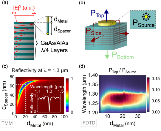
A TMM calculated 2D plot of the reflectivity at m for a wide range of both spacer () and metal layer () thicknesses is shown in Fig.1(c). A reduction in the reflectivity corresponds to coupling to an Optical Tamm State, as illustrated in the figure inset. For each nm value, there is a corresponding in the nm range which results in an OTS at 1300nm, and these two parameters are no longer independent. This reduces the dimensionality of the structural optimisation of the and , and removes any unwanted effects due to spectral detuning between the OTS and the DBR. The internal efficiency, corresponding to , obtained from 3D FDTD simulations of a 1D Tamm (where the metal layer is semi-infinite and has no radial boundary) has been shown in Fig.1(d) as a function of wavelength and metal thickness, while is set to keep the OTS wavelength constant at 1.3m. As the Tamm states are not laterally confined, the emission is highly multimoded which contributes to a broadband emission efficiency. This is not the case when a lateral confinement is introduced in the following section. It can be seen that if nm, the gold film is too thin to impedance match the 1250-1350DBR. If on the other hand nm, losses due to absorption and increased reflectivity become too large. The efficiency of m is maximised at nm, with a corresponding nm; we choose these values for the layer thicknesses moving forward.
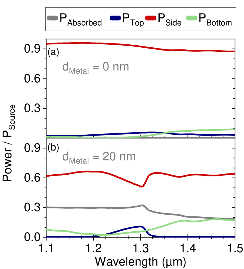
Simulations related to the planar structure of maximum efficiency are shown in figure 2. Without the metal, most light (90%) travels along the DBR, while little (5%) light is emitted vertically. On introduction of 20nm gold, the vertically emitted light at the design wavelength is increased (10%) with a concomitant increase in the absorption ( 30%). In the rest of this work we show how to reduce the absorption.
Minimising Losses for Confined Optical Tamm States
We replace the planar (infinite) metal sheets with finite-size metal discs to confine the light laterally, forming confined OTSs. The efficiency at the first lens, , is calculated for a range of discs of different diameters, , as summarised in Fig.3(a). White points denote local maxima, corresponding to the fundamental and higher order modes. As the diameter increases, the structure becomes increasingly multimoded, as expected. For a disc of diameter 2.25m, the emission into each decay channel () is shown in Fig.3(b) - the increased emission into the fundamental mode can be seen at 1.3m, accompanied by the increase in absorption and suppression of side emission. In order to discuss the far field, we represent the angle of emission relative to the structure (Fig.3(c)). In our later figures, we integrate the field intensity over the azimuthal angle.
The angular (far-field) distribution of the emitted light from the confined Tamm structures with various disc diameters is investigated. The far-field angular distribution is calculated by projecting the electromagnetic field acquired by the top monitor into the far-field by using a near-to-far field transformation. It is essential to engineer the angular distribution when the emitted light is to be coupled to other optics such as an optical fibre or an objective lens. The angular distribution of the incident light must be well within the numerical aperture (NA) of the optical instrument to achieve a high coupling efficiency. In Fig.3(d)-(g), the far-field distribution of the emission from the confined Tamm structures with different disc diameters = 2 - 5m are plotted against the emission angle and the wavelength of the light emitted by the dipole source. The numerical aperture of a standard single mode optical fibre SMF-28 (NA = 0.14) is marked by the white lines, and that of a high-NA objective lens (NA = 0.70) is marked by the orange lines. With a small gold disc (m), the emitted light from the confined Tamm structure is scattered by the edge of the metal disc into wide angles, as seen in panel (d). The angular distribution of the mode becomes more confined for large gold discs. A parabolic angular distribution (panel (g)) is seen for a very wide (5 m) confined Tamm structure, reflecting the transition to a continuum of modes for the increased disc diameter.
In between these two extremes lies a confined Tamm structure with m (panel (f)), where the radiation has a well-defined mode and is distributed close to the normal direction. It can be efficiently collected by an objective lens with NA = 0.70 (within orange lines). The emergence of the higher-order modes for large confined Tamm structures can be clearly seen from the far-field distribution. Other than the fundamental mode emitted in the normal direction, additional higher-order modes appear at shorter wavelengths with a wider emission angle.
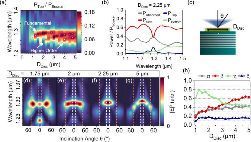
The absorption in the metal , the calculated factor, the passive emission efficiency , and the efficiency at the first lens for the fundamental mode are plotted against the disc diameter of the confined Tamm cavity in Fig.3(h). We can see that (red) increases with the disc diameter, as less light is scattered to the side for a wide confined Tamm structure. However, (green) decreases with increasing disc diameter, indicating that more light is emitted into the substrate, compared to the top surface. Moreover, the absorption in the gold disc (grey) also increases. These three factors compete and result in no significant change in the extraction efficiency (blue) with respect to the disc diameters for larger disc size. m chosen as the preferred disc diameter accounting for both the extraction efficiency (Fig.3(h)) and the far-field distribution (Fig.3(d)-(g)). For this disc diameter of 2.25 m, the first-lens efficiency of the confined Tamm structure is 18%, with a corresponding of .
Nanoring Tamm Design Principles
To reduce this substantial absorption, we introduce an aperture in the gold disc to form a nanoring structure, as schematically illustrated in Fig.4(a). Using our optimised design thus far (m, = 20 nm, = 64 nm) as a starting point, we calculate the efficiency for a range of structures with varying inner radius ; this is shown as a wavelength resolved plot in Fig.4(b) where the diameter has been shown normalised to the Tamm wavelength .
A clear enhancement in the extraction efficiency is observed when the aperture diameter is smaller than 800 nm. At = 414 nm, the efficiency is maximised. This appears close to /. Remarkably, along with the aperture diameter, the efficiency improves by a factor of almost two from 18% to 35%. Simultaneously, red-shifts from 1.296 m to 1.325 m when the increases to 0.8 m.
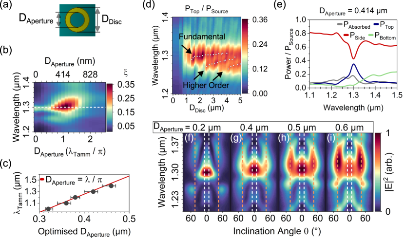
To validate the conjecture that this optimal aperture diameter is located at = /, we simulate the extraction efficiency of nanoring Tamm structures designed for a range of = 1-1.5m. To achieve different centre wavelengths, the thickness of the DBR layers and the spacer layer are appropriately varied, while the metal layer thickness is fixed to be 20 nm. The FDTD simulations are run for each nanoring Tamm structure by varying the aperture diameters from 0 to 1 m, with the outer fixed at 2.25m. Figure 4(c) shows the optimised aperture diameter for each . The optimised values agree well with = , which is shown as a red line. We note that is maximised for these different structures for aperture circumferences equal to the Tamm wavelength, which suggests hybridised annular modes from the ring.
Finally, we investigate the Tamm nanoring structure by varying the outer disc diameter , while keeping = 414 nm. The efficiency is illustrated in Fig.4(d). The modes red-shift and the structure becomes multimoded with increasing disc diameter, equivalent to the solid metal disc confined Tamm modes.
This shows the modes are only slightly perturbed by the introduction of the aperture, and that the enhancement of the emission efficiency may be caused by the hybridisation of the confined Tamm mode and the annular local mode in the aperture. Applying the 414nm () aperture to the structure described above, we present the power transmissions and , and the absorbed power for the nanoring Tamm in Fig.4(e). It can be seen that at the central , the efficiency at the first lens is nearly double () compared to that of the regular solid disc, owing to the significantly lower absorption .
We check for any aperture-induced changes on the angular distribution of the field reaching the first lens of nanoring structures with a fixed outer and a varying inner , as shown in Fig.4(f)-(i). While the aperture does induce a minor impact of the far field distribution, the majority of the emission remains within the 0.7 NA as for the solid disc considered previously.
Conclusion
Tamm structures are an intriguing form of readily manufactureable photonic cavity which are potentially suitable for both quantum and classical sources of light. However, absorption losses in the metal challenge the viability of real-world Tamm devices. In this paper, we have proposed a nanoring Tamm structure as a mechanism to increase the efficiency by reducing this absorption while maintaining a plausible far-field distribution for mode-coupling such devices.
We have shown that, for a design optimised for the telecommunications O band, replacing a traditional confined Tamm structure with a nanoring can nearly double the output power transmission, provided the aperture of the nanoring is appropriately optimised. For our design, a confined Tamm structure with outer = 2.25m results in . Introducing an aperture of (414 nm) increases to . Such an efficiency is sufficiently high for a SPS for quantum communications, and combines brightness with a highly manufactureable structure. We believe this will motivate fabrication and further research of such devices.
Author Contributions
H.H. established the idea, performed the simulations with assistance from D.D. and J.R.P., performed data analysis and drafted the paper. D.D performed supplementary simulation. E.H and R.O supervised the project. All authors were involved in the discussion and contributed to the final version of the paper.
HH thanks the Quantum Engineering Centre for Doctoral Training, and all authors acknowledge funding from EPSRC under grants META TAMM (EP/X029360/1), SPIN SPACE (EP/M024156/1), 1D QED (EP/N003381/1) in support of this research. We also acknowledge the Advanced Computing Research Centre in University of Bristol for offering the computational resources to perform the simulations.
References
- Wang et al. 2017 Wang, H. et al. High-Efficiency Multiphoton Boson Sampling. Nature Photonics 2017, 11, 361–365
- Varnava et al. 2008 Varnava, M.; Browne, D. E.; Rudolph, T. How Good Must Single Photon Sources and Detectors Be for Efficient Linear Optical Quantum Computation? Physical Review Letters 2008, 100, 060502
- O’Brien 2007 O’Brien, J. L. Optical Quantum Computing. Science 2007, 318, 1567–1570
- Vajner et al. 2022 Vajner, D. A.; Rickert, L.; Gao, T.; Kaymazlar, K.; Heindel, T. Quantum Communication Using Semiconductor Quantum Dots. Advanced Quantum Technologies 2022,
- Somaschi et al. 2016 Somaschi, N. et al. Near-Optimal Single-Photon Sources in the Solid State. Nature Photonics 2016, 10, 340–345
- Wang et al. 2019 Wang, H. et al. Towards Optimal Single-Photon Sources from Polarized Microcavities. Nature Photonics 2019, 13, 770–775
- Madsen et al. 2014 Madsen, K. H.; Ates, S.; Liu, J.; Javadi, A.; Albrecht, S. M.; Yeo, I.; Stobbe, S.; Lodahl, P. Efficient Out-Coupling of High-Purity Single Photons from a Coherent Quantum Dot in a Photonic-Crystal Cavity. Physical Review B 2014, 90, 155303
- Uppu et al. 2020 Uppu, R.; Eriksen, H. T.; Thyrrestrup, H.; Uğurlu, A. D.; Wang, Y.; Scholz, S.; Wieck, A. D.; Ludwig, A.; Löbl, M. C.; Warburton, R. J.; Lodahl, P.; Midolo, L. On-Chip Deterministic Operation of Quantum Dots in Dual-Mode Waveguides for a Plug-and-Play Single-Photon Source. Nature Communications 2020, 11, 1–6
- Liu et al. 2019 Liu, J.; Su, R.; Wei, Y.; Yao, B.; da Silva, S. F. C.; Yu, Y.; Iles-Smith, J.; Srinivasan, K.; Rastelli, A.; Li, J.; Wang, X. A Solid-State Source of Strongly Entangled Photon Pairs with High Brightness and Indistinguishability. Nature Nanotechnology 2019, 14, 586–593
- Chen et al. 2018 Chen, Y.; Zopf, M.; Keil, R.; Ding, F.; Schmidt, O. G. Highly-Efficient Extraction of Entangled Photons from Quantum Dots Using a Broadband Optical Antenna. Nature Communications 2018, 9, 2994
- Kaliteevski et al. 2007 Kaliteevski, M.; Iorsh, I.; Brand, S.; Abram, R. A.; Chamberlain, J. M.; Kavokin, A. V.; Shelykh, I. A. Tamm Plasmon-Polaritons: Possible Electromagnetic States at the Interface of a Metal and a Dielectric Bragg Mirror. Physical Review B 2007, 76, 165415
- Gazzano et al. 2011 Gazzano, O.; de Vasconcellos, S. M.; Gauthron, K.; Symonds, C.; Bloch, J.; Voisin, P.; Bellessa, J.; Lemaître, A.; Senellart, P. Evidence for Confined Tamm Plasmon Modes under Metallic Microdisks and Application to the Control of Spontaneous Optical Emission. Physical Review Letters 2011, 107, 247402
- Parker et al. 2019 Parker, M.; Harbord, E.; Chen, L.; Clarke, E.; Kennedy, K.; Rarity, J.; Oulton, R. Telecommunication Wavelength Confined Tamm Plasmon Structures Containing InAs/GaAs Quantum Dot Emitters at Room Temperature. Physical Review B 2019, 100, 165306
- Gazzano et al. 2012 Gazzano, O.; Michaelis de Vasconcellos, S.; Gauthron, K.; Symonds, C.; Voisin, P.; Bellessa, J.; Lemaître, A.; Senellart, P. Single Photon Source Using Confined Tamm Plasmon Modes. Applied Physics Letters 2012, 100, 232111
- Parker et al. 2018 Parker, M.; Harbord, E.; Young, A.; Androvitsaneas, P.; Rarity, J.; Oulton, R. Tamm Plasmons for Efficient Interaction of Telecom Wavelength Photons and Quantum Dots. IET Optoelectronics 2018, 12, 11–14
- Lundt et al. 2016 Lundt, N.; Klembt, S.; Cherotchenko, E.; Betzold, S.; Iff, O.; Nalitov, A. V.; Klaas, M.; Dietrich, C. P.; Kavokin, A. V.; Höfling, S.; Schneider, C. Room-Temperature Tamm-plasmon Exciton-Polaritons with a WSe2 Monolayer. Nature Communications 2016, 7, 13328
- Harbord et al. 2019 Harbord, E.; Cemlyn, B.; Parker, M.; Clarke, E.; Kennedy, K.; Henning, I.; Adams, M.; Oulton, R. Confined Tamm Optical States Coupled to Quantum Dots in a Photoconductive Detector. Applied Physics Letters 2019, 115, 171101
- Arakawa and Holmes 2020 Arakawa, Y.; Holmes, M. J. Progress in Quantum-Dot Single Photon Sources for Quantum Information Technologies: A Broad Spectrum Overview. Applied physics reviews 2020, 7, 21309
- Ebbesen et al. 1998 Ebbesen, T. W.; Lezec, H. J.; Ghaemi, H. F.; Thio, T.; Wolff, P. A. Extraordinary Optical Transmission through Sub-Wavelength Hole Arrays. Nature 1998, 391, 667–669
- Lezec et al. 2002 Lezec, H. J.; Degiron, A.; Devaux, E.; Linke, R. A.; Martin-Moreno, L.; Garcia-Vidal, F. J.; Ebbesen, T. W. Beaming Light from a Subwavelength Aperture. Science 2002, 297, 820–822
- Degiron et al. 2004 Degiron, A.; Lezec, H. J.; Yamamoto, N.; Ebbesen, T. W. Optical Transmission Properties of a Single Subwavelength Aperture in a Real Metal. Optics Communications 2004, 239, 61–66
- Garcia-Vidal et al. 2010 Garcia-Vidal, F. J.; Martin-Moreno, L.; Ebbesen, T. W.; Kuipers, L. Light Passing through Subwavelength Apertures. Reviews of Modern Physics 2010, 82, 729–787
- Pugh et al. 2014 Pugh, J. R.; Stokes, J. L.; Lopez-Garcia, M.; Gan, C.-H.; Nash, G. R.; Rarity, J. G.; Cryan, M. J. Slot-Grating Flat Lens for Telecom Wavelengths. Optics Letters 2014, 39, 3786–3789
- Mehfuz 2004 Mehfuz, R. Improving the Excitation Efficiency of Surface Plasmon Polaritons near Small Apertures in Metallic Films. Ph.D. thesis, 2004
- Gordon and Ahmed 2018 Gordon, R.; Ahmed, A. Reaching the Limits of Enhancement in (Sub)Nanometer Metal Structures. ACS Photonics 2018, 5, 4222–4228
- Shafiq et al. 2022 Shafiq, R.; Iqbal, J.; Khan, A. D.; Rehman, A. U. A Theoretical Study of Broadband Extraordinary Optical Transmission in Gold Plasmonic Square Nanohole Arrays and Its Application on Refractive Index Sensor. Optical and Quantum Electronics 2022, 54, 156
- Wang et al. 2022 Wang, Z.; Kapsalidis, F.; Wang, R.; Beck, M.; Faist, J. Ultra-Low Threshold Lasing through Phase Front Engineering via a Metallic Circular Aperture. Nature Communications 2022, 13, 230
- Trojak et al. 2017 Trojak, O. J.; Park, S. I.; Song, J. D.; Sapienza, L. Metallic Nanorings for Broadband, Enhanced Extraction of Light from Solid-State Emitters. Applied Physics Letters 2017, 111, 021109
- Haws et al. 2022 Haws, C.; Perez, E.; Davanco, M.; Song, J. D.; Srinivasan, K.; Sapienza, L. Broadband, Efficient Extraction of Quantum Light by a Photonic Device Comprised of a Metallic Nano-Ring and a Gold Back Reflector. Applied Physics Letters 2022, 120, 081103
- Afinogenov et al. 2013 Afinogenov, B. I.; Bessonov, V. O.; Nikulin, A. A.; Fedyanin, A. A. Observation of Hybrid State of Tamm and Surface Plasmon-Polaritons in One-Dimensional Photonic Crystals. Applied Physics Letters 2013, 103, 061112
- Lopez-Garcia et al. 2014 Lopez-Garcia, M.; Ho, Y.-L. D.; Taverne, M. P. C.; Chen, L.-F.; Murshidy, M. M.; Edwards, A. P.; Serry, M. Y.; Adawi, A. M.; Rarity, J. G.; Oulton, R. Efficient Out-Coupling and Beaming of Tamm Optical States via Surface Plasmon Polariton Excitation. Applied Physics Letters 2014, 104, 231116
- Azzini et al. 2016 Azzini, S.; Lheureux, G.; Symonds, C.; Benoit, J.-M.; Senellart, P.; Lemaitre, A.; Greffet, J.-J.; Blanchard, C.; Sauvan, C.; Bellessa, J. Generation and Spatial Control of Hybrid Tamm Plasmon/Surface Plasmon Modes. ACS Photonics 2016, 3, 1776–1781
- Symonds et al. 2017 Symonds, C.; Azzini, S.; Lheureux, G.; Piednoir, A.; Benoit, J. M.; Lemaitre, A.; Senellart, P.; Bellessa, J. High Quality Factor Confined Tamm Modes. Scientific Reports 2017, 7, 1–7
- Zheng et al. 2019 Zheng, Y.-d.; Xiao, F.-a.; Liu, W.-j.; Hu, X.-l. Purcell Effect and Light Extraction of Tamm-plasmon-cavity Green Light-Emitting Diodes. Optics Express 2019, 27, 30852
- Pugh et al. 2021 Pugh, J. R.; Harbord, E. G. H.; Sarua, A.; Fletcher, P. S.; Tian, Y.; Wang, T.; Cryan, M. J. A Tamm Plasmon-Porous GaN Distributed Bragg Reflector Cavity. Journal of Optics 2021, 23, 035003
- Sarua et al. 2023 Sarua, A.; Pugh, J. R.; Harbord, E.; Cryan, M. J. Enhancement of InGaN Quantum Well Photoluminescence in a Tamm Metal/Porous-DBR micro-Cavity. IEEE Photonics Journal 2023, 1–7
- Yang et al. 2017 Yang, Z.-Y.; Ishii, S.; Yokoyama, T.; Dao, T. D.; Sun, M.-G.; Pankin, P. S.; Timofeev, I. V.; Nagao, T.; Chen, K.-P. Narrowband Wavelength Selective Thermal Emitters by Confined Tamm Plasmon Polaritons. ACS Photonics 2017, 4, 2212–2219
- Symonds et al. 2013 Symonds, C.; Lheureux, G.; Hugonin, J. P.; Greffet, J. J.; Laverdant, J.; Brucoli, G.; Lemaitre, A.; Senellart, P.; Bellessa, J. Confined Tamm Plasmon Lasers. Nano Letters 2013, 13, 3179–3184
- Toanen et al. 2020 Toanen, V.; Symonds, C.; Benoit, J.-M.; Gassenq, A.; Lemaî, A.; Bellessa, J. Room-Temperature Lasing in a Low-Loss Tamm Plasmon Cavity. ACS Photonics 2020, 7, 2952–2957
- Vinogradov et al. 2006 Vinogradov, A. P.; Dorofeenko, A. V.; Erokhin, S.; Inoue, M.; Lisyansky, A. A.; Merzlikin, A. M.; Granovsky, A. Surface state peculiarities in one-dimensional photonic crystal interfaces. Physical Review B 2006, 74