Evaluating the transport properties of interface-type, analog memristors
Abstract
Interface-type, analog memristors have quite a reputation for real-time applications in edge sensorics, edge computing, and neuromorphic computing. The n-type conducting BiFeO3 (BFO) is such an interface-type, analog memristor which is also nonlinear and can therefore not only store, but also process data in the same memristor cell without data transfer between the data storage unit and the data processing unit. Here we present a physical memristor model which describes the hysteretic current-voltage curves of the BFO memristor in the small and large current-voltage range. Extracted internal state variables are reconfigured by the ion drift in the two write branches and are determining the electron transport in the two read branches. Simulation of electronic circuits with the BFO interface-type, analog memristors was not possible so far because previous physical memristor models have not captured the full range of internal state variables. We show quantitative agreement between modeled and experimental current-voltage curves exemplarily of three different BFO memristors in the small and large current-voltage ranges. Extracted dynamic and static internal state variables in the two full write branches and in the two full read branches, respectively, can be used for simulating electronic circuits with BFO memristors, e.g. in edge sensorics, edge computing, and neuromorphic computing.
I Introduction
The advent of the Internet of Things (IoT) has transformed our technologically interconnected society, leading to a surge in the demand for computational resources. This increase in computational needs is intimately linked with a growth in energy consumption, a situation that is becoming increasingly untenable as we approach the limitations defined by Moore’s law. Consequently, the pursuit of more efficient computational methodologies has become imperative for the next phase of technological advancement. Research has pointed to innovative pathways such as the development of improved algorithms [1, 2, 3] and the exploration of alternative memory elements [4, 5, 6] that deviate from conventional semiconductor technology. Such alternative memory elements are one of the core enabler for novel artifical intelligence (AI) accelerator hardware. AI design needs to handle a lot of design corners, e.g. the development of physical models describing the new core enabler hardware. Within this context, memristors have emerged as a promising solution.
Memristors serve as pivotal elements with extensive applicability [7, 8, 9, 10] in advancing the domains of AI [11, 12], neural networks [13, 14] and secure electronics [15, 16]. In particular, the Bismuth iron oxide BiFeO3 (BFO) has attracted attention as an important material for interface-type, analog, and non-linear memristors [17, 18]. BFO thin films are intrinsically n-type conducting due to the formation of oxygen vacancy donor ions during fabrication. The hysteretic current-voltage characteristics of BFO memristors reveal four current-voltage branches, two full reconfigurable write branches with dynamic internal state variables and two full unaltered read branches with static internal state variables [H. Schmidt, private communication]. Oxygen vacancies in BFO thin films with two metallically conducting electrodes tend to drift in an electric field, e.g., when a so-called write bias is applied to the metallically conducting electrodes [19]. The oxygen vacancies are displaced in the two full write branches in the hysteretic current-voltage curves of BFO memristors and in the same time the quasi-Fermi level is reconfigured and the internal state variables of the BFO memristor are changed. The BFO memristor shows a changing memristance in the two full write branches. Furthermore, due to the non-linear current voltage curves, the resistance of the BFO memristor is continuously changed in the two full read branches. So far there exists no simulation in agreement with experimental hysteretic current-voltage curves which accounts for changing/unchanging internal state variables of BFO memristors in the two full write branches/two full read branches at both large and small voltages. E.g., the study by Chen et al. [20] only addressed the modelling of resistive switching in BFO memristors at large voltages of the hysteretic current-voltage curves. And in the study by Yarragolla et al. [21], the modelling of resistive switching in BFO memristors assumed changing of internal state variables not only in the two full write branches but also in the two full read branches. This results in inconsistencies pertaining to the reconfiguration of the quasi-Fermi level and to the modulation of the Schottky barrier height of the two metallically conducting electrodes attached to the BFO memristor. Model presented here correctly describes that the Schottky barrier height can be reconfigured only in the two full write branches and not in the two full read branches. For advancing the development of electronic circuits with BFO memristors a clear understanding of the dependence of internal state parameters on the operation of BFO memristors is necessary [22]. The physical memristor model of hysteretic current-voltage curves of interface-type memristors has to account for the dominating ion drift in the two write branches and its influence on the internal state variables which determine the electron drift in the two read branches. Such a model will pave the way for novel electrical and electronic devices with BFO memristors that merge data processing and storage in the same device cell, essentially combining memory and processing without data transfer between memory and processor. Building on this, we propose a physical memristor model where the internal state variables only change in the two complete write branches, leaving the read branches unaffected. This new approach accurately reproduces the hysteretic IV characteristics of n-type conducting, interface-type memristors in both small and large bias ranges and aligns the tendencies of the reconfigurable Schottky barrier height with theoretical band alignment predictions.
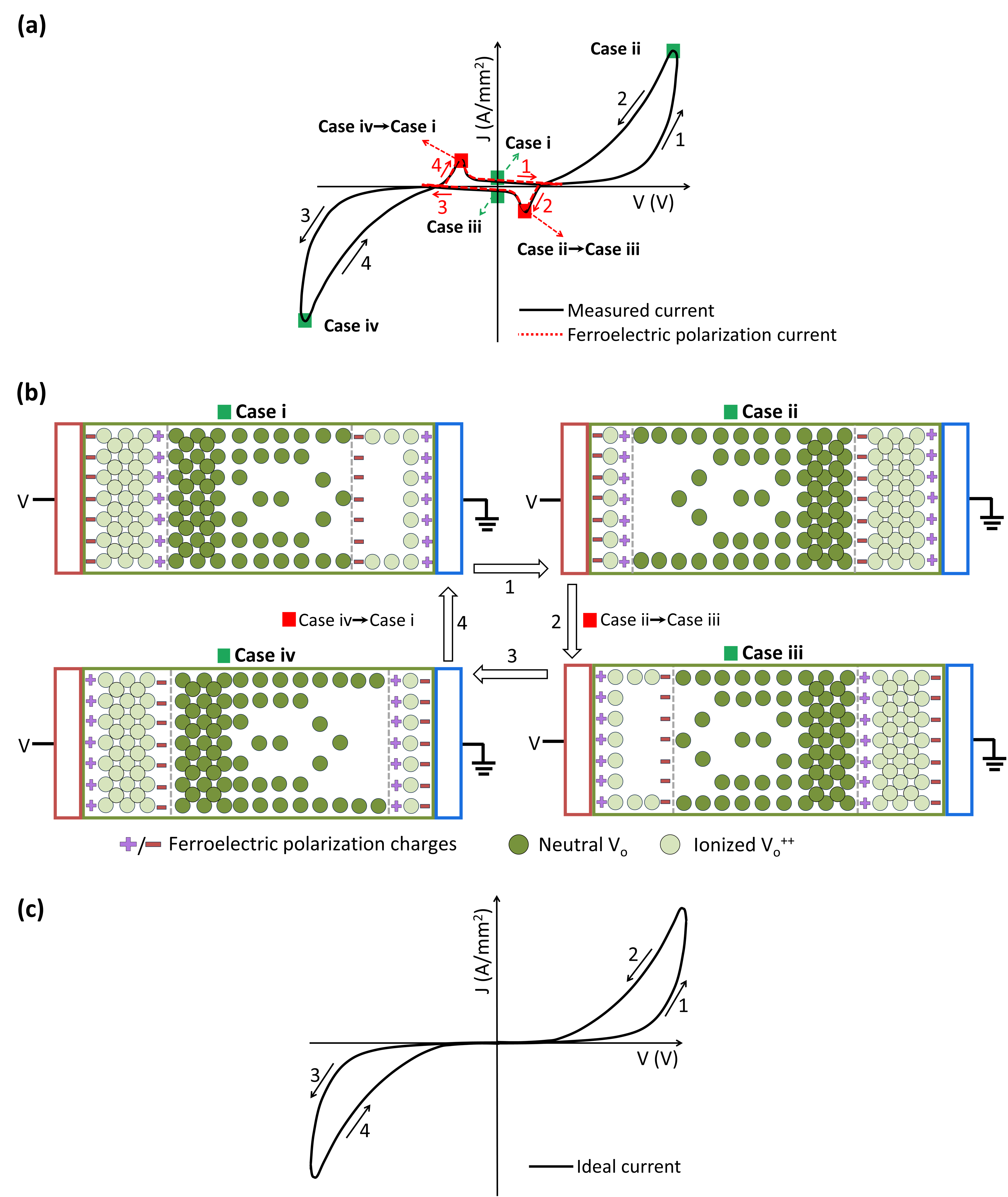
Figure 1 offers an insightful perspective into the read and write operation of BFO memristors. BFO is a multiferroic material with ferroelectric ordering (ferroelectric Curie temperature [23]) and antiferromagnetic ordering (antiferromagnetic Néel temperature [24]). When a voltage is sourced to operate the BFO memristor below the ferroelectric Néel temperature, spontaneous electric polarization can be reversed and a polarization switching current flows [25]. In this work, we exclusively focus on the change of internal state variables due to the redistribution of oxygen vacancies in BFO memristors with ideal current ()-voltage () characteristics curves under the electric field in the two write branches. Presented physical memristor model is applied to hysteretic current-voltage curves. Ideal current-voltage hysteresis curves (Fig. 1 c) are obtained from experimental current-voltage hysteresis curves (Fig. 1 a) by subtracting the contribution of possible polarization currents due to ferroelectric switching from experimental hysteretic current-voltage curves [26]. The current flows when the voltage is ramped. The current density , , with being the area of top electrode (TE) of BFO memristors is also introduced because we also extract internal state parameters being independent of the area of the TE. Experimental current density-voltage curves (Fig. 1 a) and ideal current density-voltage curves (Fig. 1 c) are shown. We use ideal - hysteresis loops to extract the internal state variables based on the simulation. We also present the unique aspects of oxygen vacancy drift in BFO memristor interface switching with the metallic conducting TE and the metallic conducting bottom electrode (BE), the TE and BE form a Schottky contact on the BFO thin film where they are attached. The extension of the depletion layer is indicated with a grey scattered line in Fig. 1 (b). Fig. 1 (a) depicts the measured - characteristic which is used to extract the ideal - characteristics by subtracting the polarization current density due to ferroelectric switching (Fig. 1 (c)). Notably, the ideal - curve is divided into four branches: Branch 1 and Branch 3 act as write branches, allowing modification to the internal state of the memristor, while Branch 2 and Branch 4 serve as read branches for retrieving the internal state which have been written in Branch 1 and Branch 3, respectively. This partitioning is essential in comprehending the underlying operational principles of the BFO memristor. Accompanying the - curve, visualization of the distribution of mobile oxygen vacancies () in these different branches under various biases is explicitly depicted in Fig. 1 (b). In particular, the figure portrays neutral oxygen vacancies () in the undepleted region and ionized oxygen vacancies in the depletion layer (). Oxygen vacancies only drift in an electric field in Branch 1 and Branch 3. They drift in the direction of the electric field and are continuously redistributed after a threshold electric field strength. The final distribution of ionized oxygen vacancies depends on the voltage vs time ramping profile () in branches 1 and 3. If the internal state parameter at the beginning of a write branch is the same, then always the same memristance curve (flux-charge) will be recorded for the same memristor. It does not matter how a given distribution of ionized oxygen vacancies is reached.
In our study, we investigate four distinct current-voltage branches 1-4. The four IV branches differ with respect to the distributions of polarization charges and oxygen vacancies in BFO memristors. The analysis yields internal state variables of BFO memristors in the four IV branches 1-4. Armed with these insights into the internal state variables, it will become feasible to design and develop electronic circuits with BFO memristors that unify data processing and storage functionality in the same cell without data transfer [27], while also successfully suppressing ferroelectric switching, thereby enhancing their applicability and performance. In more insulating conventional BFO thin films scenarios, the ferroelectric current predominantly manifests within the insulating region [28], particularly in the area defined as the depletion region. It typically occurs when there is an incremental increase in the potential applied across the ferroelectric material. Contrary to this established behavior, our observations reveal an intriguing anomaly: the insulating region in our investigation is synonymous with the depletion region at the TE and BE which form a Schottky contact. Given that the potential within this region is inversely related to the applied potential, the ferroelectric current is found to emerge as the applied potential diminishes [20]. This unexpected phenomenon presents a novel aspect of ferroelectric current behavior, opening a new dimension in our understanding of the underlying mechanics and may carry substantial implications for the design and operation of multiferroic memristors with interface switching where ferroelectric switching and its contribution to the current-voltage characteristics need to be suppressed, e.g., by random alignment of ferroelectric polarization in polycrystalline multiferroic memristors [29]. The multifaceted insights provided by Fig. 1 serve as a vital framework for future exploration and application in the field of memristor technology, as well as in the realm of multiferroic materials and oxygen vacancies drifting under the electric field in the write operation.
II Modeling
From now on we use area independent internal state variables which are extracted from the current density J vs. voltage curves. When examining the relationship between current density - voltage characteristics of BFO memristors, we denote the layer structure of BFO memristor as TE/BFO/BE, with TE representing the top electrode, BFO representing the BFO layer, and BE representing the bottom electrode. Both junctions, the top electrode junction (TE/BFO) and the bottom electrode junction (BFO/BE) function as Schottky barriers (Fig. 1). Schottky barriers (Fig. 2) play an instrumental role in the electronic properties of metal-semiconductor devices. In Fig. 2, we specify the TE material as Au and the BE material as Pt/Ti. Specifically, in the TE/BFO/BE heterostructure, potential barriers emerge at the interfaces between the gold (Au) top electrode (TE) and the n-type semiconductor BFO, as well as between BFO and the Pt/Ti bottom electrode (BE). When a metal, like Au with a work function of [30], or Pt with a work function of [31], contacts the n-type semiconductor BFO with [32], electron migration occurs from the semiconductor to the metal until equilibrium is reached through Fermi level alignment. In the presented figure 2, the intricate energy band dynamics of a TE/BFO/BE heterostructure are meticulously showcased. Initial sections (a) to (d) provide comprehensive band diagrams depicting the transition and evolution of electronic states across different branches. Subsequently, (e) and (f) sections offer insights into the influence of oxygen vacancy concentration on the energy difference within the BFO at the interfaces and the barrier height parameters. This visualization is paramount in comprehending the correlation between susceptibility of BFO, work functions, Fermi levels, and barrier heights. The color coding further simplifies the understanding, wherein the top electrode (TE), the n-type semiconductor (BFO), and the BE are represented in shades of red, green, and blue respectively. The figure’s comprehensive representation is pivotal for grasping the advanced principles and nuances of TE/BFO/BE heterostructures, presenting it as a cornerstone for researchers and experts in the domain.
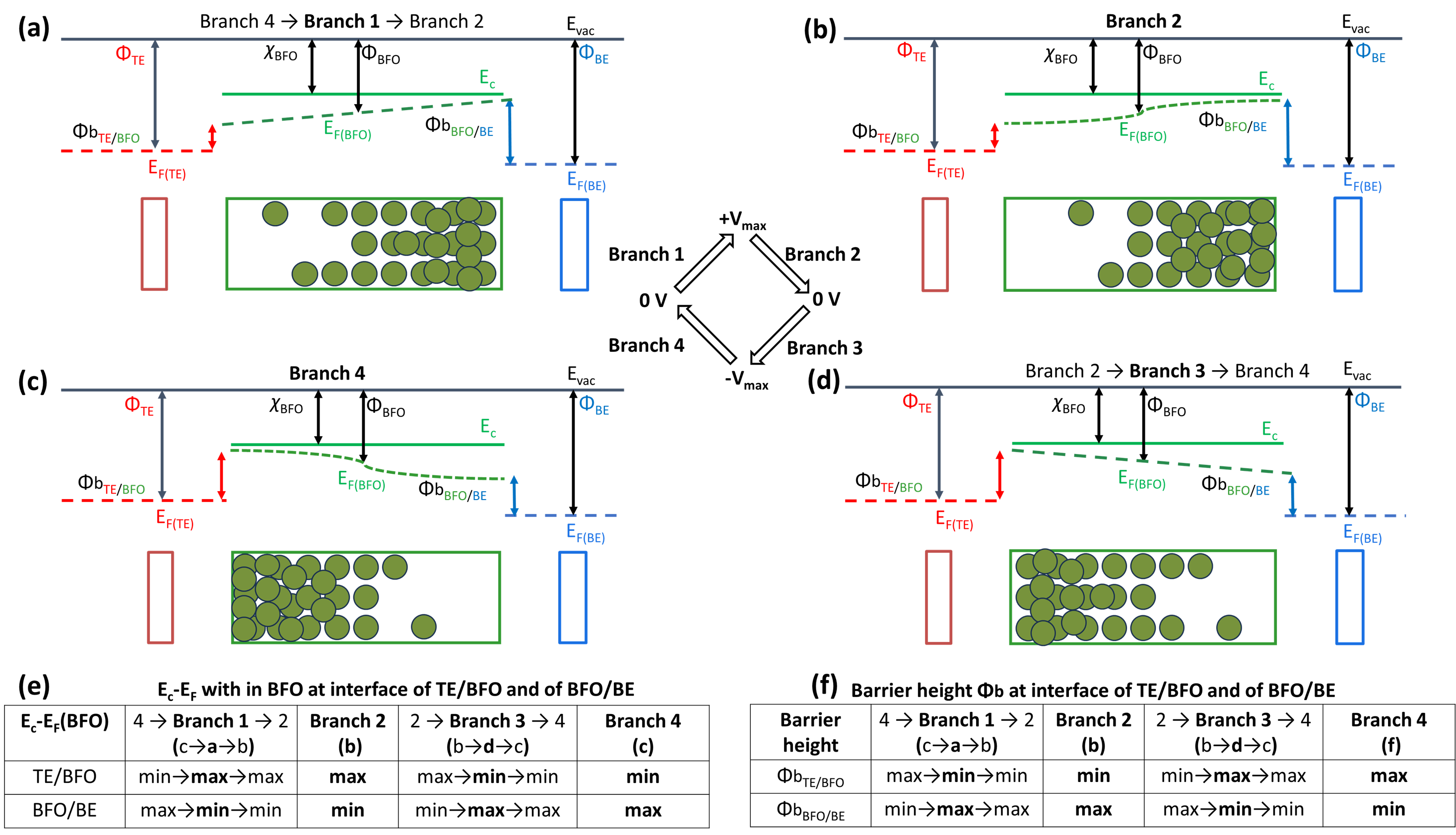
The Schottky barrier’s magnitude, , is determined by the energy difference between the metal’s work function ( or ) and the electron affinity of the semiconductor. The energy differences and the barrier heights are listed in the tables of Fig. 2e and Fig. 2f. The barrier heights at the interfaces of Au/BFO and BFO/Pt/Ti are symbolized as and respectively. Furthermore, the Schottky barrier height is influenced by the distribution of oxygen vacancies in BFO, i.e., by the position-dependent oxygen vacancy concentration. Because oxygen vacancies are intrinsic donors in BFO, when being redistributed they consequentially modify the alignment of the quasi-Fermi level in n-BFO (Fig. 2a-d). Therefore, the energy difference between the conduction band edge and the Fermi level in BFO, labeled as , is regulated by the oxygen vacancy distribution. In essence, the Schottky barriers at the Au/BFO and BFO/Pt/Ti interfaces significantly impact the electronic properties of the heterostructure. Their heights are not only contingent upon the materials’ work functions but are also affected by internal factors like the oxygen vacancy distribution and the donor-quasi Fermi level concentrations in BFO. Comprehensive understanding of these potential barriers is pivotal for predicting and enhancing the performance of devices stemming from such TE/BFO/TE layer structures.
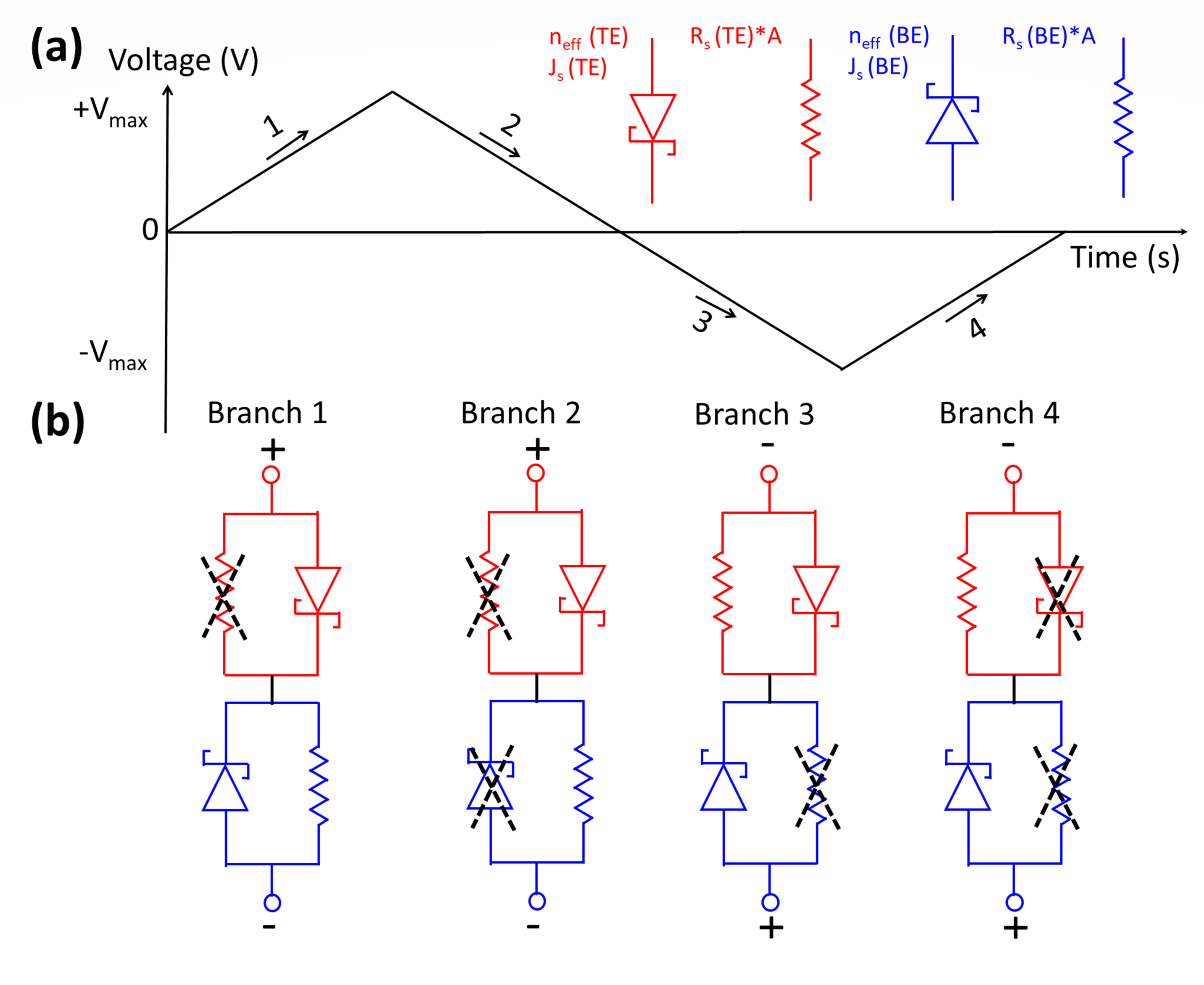
Fig. 3(a) shows an example a linear voltage -time profile. The voltage-time profile determines the dynamics of internal parameter changes in the two full write branches. However, it does not influence the internal parameters in the two full read branches with their unique relation between applied voltage and applied current which does not depend on the charge flown and the history of the voltage during read operation. Applied voltage sweep is classified into four current-density branches, 1 (Branch 1, 0 to +), 2 (Branch 2, + to 0), 3 (Branch 3, 0 to -) and 4 (Branch 4, - to 0). The corresponding equivalent circuits are shown in Fig. 3(b) and used to model measured current density – voltage curves of three BFO memristors [Fig. 2 in [27]].
In the analysis of the Schottky barrier contact interface, the equivalent circuit illustrated in Fig. 3(b) is characterized by incorporating a parallel leakage resistor (), which exhibits an inverse relationship with the oxygen vacancy concentration adjacent to the barrier [33, 34]. This depiction of leakage resistance offers a more accurate physical representation than considering changes in barrier height caused by the accumulation of oxygen vacancies. The prominent physical parameters describing the Schottky barriers are the reverse saturation current density () and the ideality factor (). These parameters are integrated into the Schottky barrier equation, , as follows:
| (1) |
where , , , , , , , and are barrier potential, current density, reverse saturation current density, the charge of an electron, voltage drop across the barrier, ideality factor, Boltzmann constant, and temperature. The reverse saturation current density () provides insight into the minority carrier activities, while the ideality factor (n) quantifies the divergence of the Schottky diode’s real behavior from the ideal Schottky diode.
In the present study, we also address the influence of the position dependent quasi-Fermi energy in the n-type BFO layer as demonstrated in the energy band diagrams of Fig. 2, on the ideality factor . It has been observed that is contingent upon the recombination mechanisms and remains constant provided that the energy difference between the conduction band minimum and the donor quasi-Fermi energy within the BFO remains uniform throughout. However, as the energy diagrams in Fig. 2 parts (a) and (d) indicate, the presence of oxygen vacancy drift introduces variability in at the interface of the TE/BFO/BE layer structure. This variation and also the varitaion of in (b) and (c) necessitates a revision of the conventional ideality factor to incorporate a dependency on the applied voltage, as the band alignment changes dynamically fluctuates due to the dynamic drift of oxygen vacancies. Consequently, a modification to the ideality factor is proposed as a function of voltage, allowing for a more nuanced understanding of the Schottky barrier behavior in the presence of non-uniform oxygen vacancy distribution in the BFO layer and resulting non-uniform alignment of the donor-quasi Fermi level (Fig. 2).
Instead of relating the ideality factor with the total applied voltage across the TE/BFO/BE structure, we introduce a current density () dependent effective ideality factor, denoted as . This effective ideality factor accounts for the voltage drop across the specific contact under investigation. The relationship between the effective ideality factor and the applied voltage and current density is given as follows:
| (2a) | ||||
| where | ||||
| (2b) | ||||
Here, is the conventional ideality factor from Eq. 1 and [] is the proportionality constant. This reformulation offers a more targeted description of the device behavior, thereby enhancing the precision of the modeling and analysis specific to the contact configuration of interest. This novel approach paves the way for more accurate simulations and optimizations in various applications where the understanding of contact-specific behavior is crucial.
The TE/BFO junction is modeled as a forward-biased Schottky diode (FB), and the BFO/BE junction as a reverse-biased Schottky diode (RB), under conditions where the TE is positively biased and the BE is grounded (Fig. 3(b), Branch 1 and Branch 2). Conversely, when the TE is negatively biased and the BE is grounded, the TE/BFO junction is represented by a reverse-biased(RB) Schottky diode and the BFO/BE junction by a forward-biased (FB) Schottky diode (Fig. 3(b), Branch 3 and Branch 4).
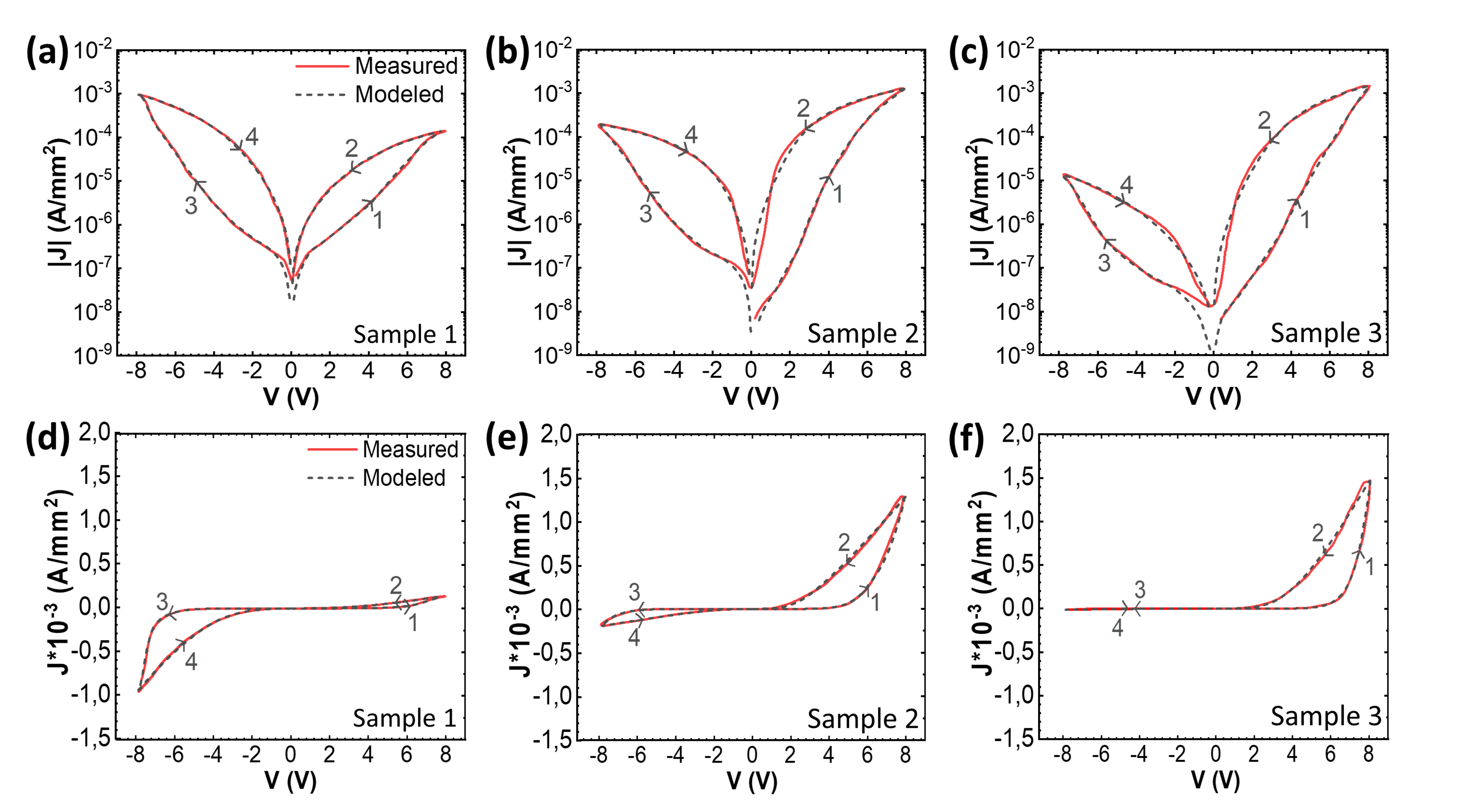
Fig. 4 shows double hysteresis switching characteristics of BFO memristor samples. The measured I-V data was taken from T. You et al. [27]. BFO memristor shows an interface switching, the physical model parameters presented do not depend on the area of TE and BE. Therefore, we took the area (A =4.53 10-2 mm2) of TE to model the current density J (J=I/A) - voltage (V) (red solid lines) characteristics and extract the physical model parameters in terms of J and R.A. The branches corresponding to WRITE branches are 1 & 3 and READ branches are 2 & 4. WRITE branches are characterized by the application of high-voltage ramping and the memristor is switched from one stable state (high resistance state) to the other (low resistance state). By applying opposite polarity, the resistance state (low resistance state) of READ branches (2,4) can be reversed. A circuit model is developed with a set of Eq’s. 3 to simulate the effect of different distributions on the oxygen vacancies on the switching characteristics of BFO samples. In the following, we apply presented simulation model to the current density-voltage hysteresis loops of three different BFO memristors. We call J-V curves with a hysteresis in the first and third J-V quadrant double J-V hysteresis. Those BFO memristors with double J-V hysteresis have been fabricated and investigated in a previous work [27] to demonstrate the reconfigurability of BFO memristors into the 16 Boolean logic gates. This was an important step towards data processing and storage in the same memristor device without data transfer. However, only now one can estimate the power consumption, speed, size and cost of electronic circuits with BFO memristors using the presented physical model for electronic design automation simulations. The experimental current density-voltage hysteresis loops of three the different BFO memristors presented only in Ref. [27] contain small contributions from the ferroelectric polarization current density. We removed the ferroelectric polarization current density and obtained an ideal current density (Fig. 1). In the following we report in detail on the extraction of the internal state variables (Fig. 3b) from the double J-V hysteresis with, branches 1-4 (Fig. 1c).
A comprehensive investigation of the double J-V hysteresis (Fig. 4) reveals two prominent resistance states, necessitating two distinct input signals for transition between them, as evidenced by the experimental data in Ref. [27]. The measured J-V characteristic curves of sample 1, sample 2, and sample 3 from You et al. [27] are depicted in Fig. 4(a-c) on a logarithmic scale and in Fig. 4(d-f) on a linear scale, after the subtraction of ferroelectric current density if necessary. Actually, the ferroelectric contribution of sample 1 and sample 3 is negligible and only the J-V curve of sample 2 shows a contribution from the ferroelectric polarization current in the small voltage range. We provide an ideal current density-voltage (J/V) data set, derived from the data as initially reported in You et al. [27]. Branch labels, 1-4, have been included in both types of representations. The behavior of the memristor can be partitioned into two diodes, specifically, the forward bias (FB) diode and the reverse bias (RB) diode, which is expressed by the following equation:
| All Branches: | ||||
| (3a) | ||||
| (3b) | ||||
| (3c) | ||||
| (3d) | ||||
In Eq. (3), we present a comprehensive mathematical description of the current density ()-voltage () characteristics of a memristor, modeled as a series combination of a forward bias (FB) diode and a reverse bias (RB) diode. The effective ideality factors for the reverse and forward biased diodes are represented by and , respectively, as shown in Eqs. (3a) and (3c). These effective ideality factors incorporate both the original ideality factors ( and ), the proprtionality factors ( and ), and the thermal voltage (), modified by the current density () and the saturation current densities ( and ) of the respective diodes similar to Eqn. 2b.
In equation (3b), the current density through the reverse biased diode () is expressed as a function of the applied voltage across the reverse biased diode (), the effective ideality factor (), and the saturation current density ().
Finally, the overall voltage () across the memristor is described in equation (3d) as a function of the current density (), the effective ideality factor (), the saturation current density (), the current density through the reverse biased diode (), the resistance of the reverse biased diode (), and the area of the top electrode ().
Together, these equations provide a comprehensive mathematical framework with physical parameters for understanding and modeling the electrical characteristics of write and read states of memristors, represented as a series combination of forward and reverse biased diodes.
-
1.
Write Branch 1 and 3: The write branches are characterized by the redistribution of oxygen vacancies under applied write voltage. In write branch 1 oxygen vacancies are drifting from the TE to the BE. And in write branch 3 the oxygen vacancies are drifting from the BE to the TE. The redistribution of oxygen vacancies changes the alignment of the quasi-fermi level in BFO with respect to the conduction band minimum and with that also the internal state parameter of the barrier height at the TE/BFO and at the BFO/BE interface. The other changing internal parameters are , , and as a function of current density in equations 3.
-
2.
Read Branch 2 and 4: This voltage does not redistribute the oxygen vacancies as long as maximum amplitude of read voltage is not larger than the maximum voltage of previously applied write voltage. Distribution of oxygen vacancies will only occur if a voltage of opposite polarity in comparison to the previously applied write voltage is applied to the BFO memristor. This again corresponds to the voltage ramping in a write branch. The current density at any voltage is accurately described by the internal state parameters, i.e., by the internal state variables at the largest bias of branch 1 for branch 2 and by the internal state variables at the largest bias of branch 3 for branch 4: and . However, the ideality factor here is dependent on the voltage drop across the forward bias Schottky contact (eqn. 2).
III Methods
The fitting procedures for branch 1-4, as delineated in Equation 3, were executed using Python in distinct methodologies to optimize accuracy and efficiency. Read branch 2, defined in Equation 3b, and read branch 4, as per Equation 3d, were subject to an automated fitting process. This approach leveraged the least_squares function in Python, a robust optimization tool commonly employed in computational data analysis. The function iteratively minimized the residuals between the observed data and the model predictions, adjusting the parameters to best fit the empirical observations. Conversely, write branch 1 (Equation 3a) and write branch 3 (Equation 3c) necessitated an iterative manual fitting approach. Such a manual approach is particularly beneficial in cases where the model behavior is complex or non-linear, as it permits a more tailored fit to the dataset.
IV Results
The interface switching in memristors is affected by the physical properties of the memristor material involved, and the relationships between the current density J and voltage V. The internal state variables of the memristor are crucial to understand its behavior and to develop electronic circuits with memristors, e.g. AI accelerators. The presented equations in the appendix Eqns. 4, 5, 6 and 7 and the parameters listed in Tab. 1 are related to the analysis of interface switching in three different BFO memristors.
The table provided (Table 1) presents a comprehensiveoverview of the physical model parameters pertaining to the three BFO memristors (Samples 1-3) as they relate to four operational branches (, , , ). These branches represent the intricate interactions occurring at the interfaces of the Top Electrode (TE)/BFO and BFO/Bottom Electrode (BE) under varying bias conditions, encompassing both forward and reverse biases. It is worth highlighting that the parameters and employed in our modeling are intricately linked to the effective parameter , as elaborated in Eq. 2.
| TE/BFO | BFO/BE | BFO/BE | TE/BFO | |||||||||
| (1 & 2 TE:FB, 3 TE:RB) | (1 & 2 BE:RB) | (3 & 4 BE:FB, 1 BE:RB) | (3 & 4 TE:RB) | |||||||||
| Branch | ||||||||||||
| V-1 | V-1 | |||||||||||
| Sample 1 | ||||||||||||
| 1 | 32.00 | 0.30 | 540.84 | +0.45 | 21.34 | -0.81 | 4.88 | 0.01 | 234.00 | - | - | - |
| 2 | 24.00 | 2.75 | 540.84 | - | 21.34 | - | - | - | - | - | - | - |
| 3 | 24.00 | 60.00 | 540.84 | - | - | - | 23.00 | 0.40 | 234.00 | +0.40 | 2.58 | -0.99 |
| 4 | - | - | - | - | - | - | 4.88 | 19.6 | 234.00 | - | 2.58 | - |
| Sample 2 | ||||||||||||
| 1 | 16.00 | 0.20 | 624.72 | +0.65 | 3.64 | -0.80 | 11.40 | 6500.00 | 206.62 | - | - | - |
| 2 | 15.80 | 0.33 | 624.72 | - | 3.64 | - | - | - | - | - | - | - |
| 3 | 15.80 | 4000.00 | 624.72 | - | - | - | 16.00 | 0.15 | 206.62 | +0.20 | 25.55 | -0.93 |
| 4 | - | - | - | - | - | - | 11.40 | 2.42 | 206.62 | - | 25.55 | - |
| Sample 3 | ||||||||||||
| 1 | 19.00 | 0.16 | 103.09 | +0.30 | 2.17 | -0.90 | 6.85 | 0.1 | 7.04 | - | - | - |
| 2 | 9.24 | 4.50 | 103.09 | - | 2.17 | - | - | - | - | - | - | - |
| 3 | 9.24 | 1200.00 | 103.09 | - | - | - | 19.00 | 3.30 | 7.04 | +0.25 | 126.84 | -1.10 |
| 4 | - | - | - | - | - | - | 6.85 | 18.10 | 7.04 | - | 126.84 | - |
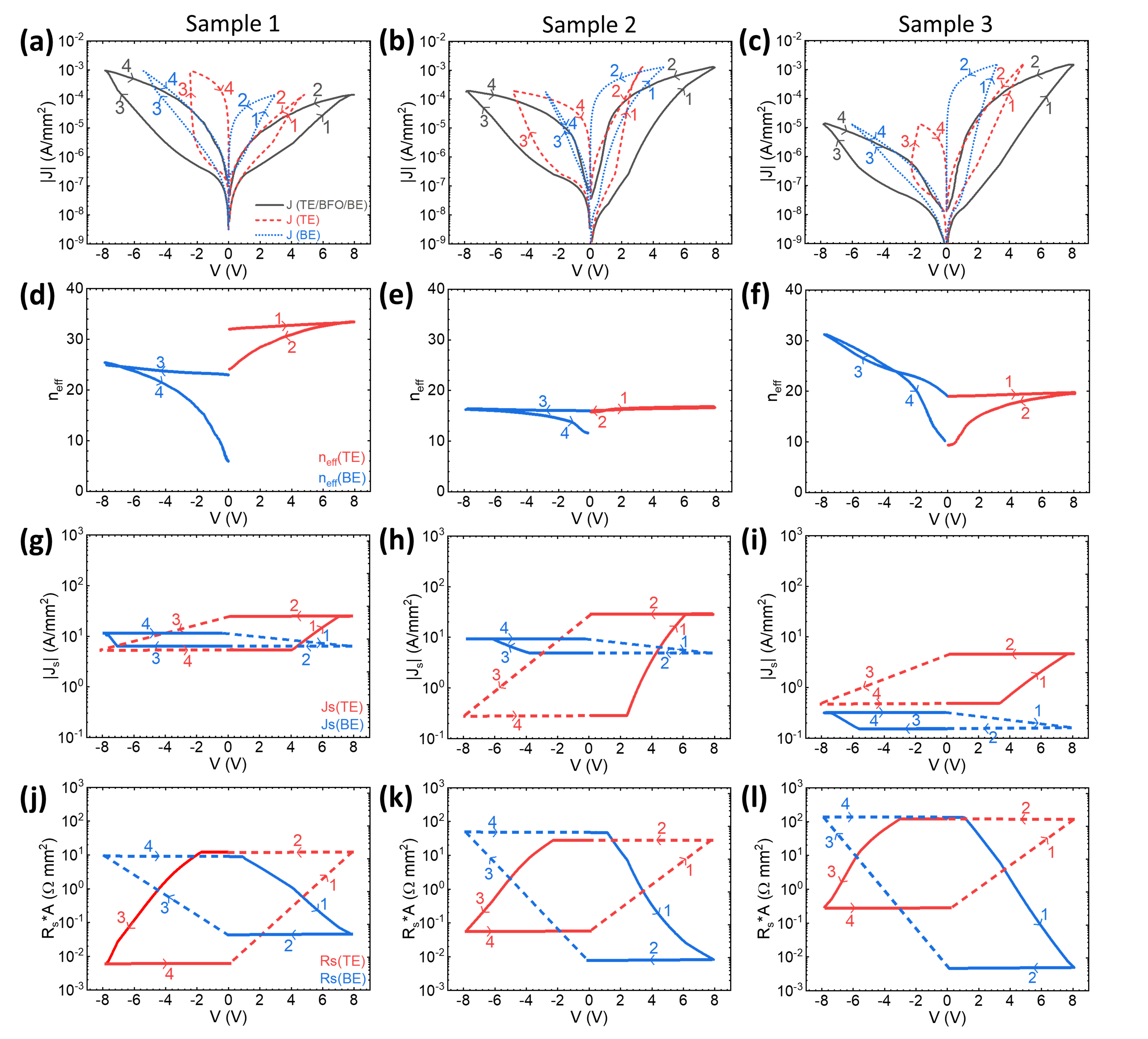
Specifically, within branches and , the TE/BFO interface operates as a forward bias diode (FB), while the BFO/BE interface functions as a reverse bias diode (RB) (Refer to Eqns. (4)-(7)). Conversely, in branches and , this configuration is reversed, with the TE/BFO acting as RB and BFO/BE as FB diodes. In the context of branches and , it is noteworthy that the parameters , , , and exhibit no discernible variation in response to applied voltage changes. These parameters remain constant, underscoring their stability in these specific operational conditions. In contrast, within branches and , we observe that the parameters , , and for the RB diode remain unchanged over small voltage ranges, typically below 2 V. Furthermore, above 2 V, any variation in these parameters with applied voltage is deemed negligible for our modeling purposes. Notably, the parameters and for the FB diode hold validity across all voltage ranges in these branches and remain unaltered by changes in applied voltage.
It is crucial to emphasize that the voltage-dependent parameters in these branches are (FB) and (RB). We observe that the logarithm of is directly proportional to the logarithm of , while the logarithm of is directly proportional to the negative logarithm of . The precise proportionality constants governing these relationships are meticulously documented in Table 1, as and , respectively. For a given cycle of resistive switching (RS) in 2D memristors, which exhibit significant cycle-to-cycle (C2C) variability, Spetzler et al. [35] also determined a proportionality constant between and [35]. Given the negligible C2C variability in BFO memristors, all parameters in Table 1, including the proportionality constant between and , are applicable for all cycles of RS in BFO memristors. It is noteworthy that as voltage increases, the barrier height of the FB diode decreases ( increases), while the leakage resistance of the RB diode decreases correspondingly. Consequently, there exists an inverse relationship between the leakage resistance of the RB diode and the barrier height of the RB diode, with both parameters exhibiting voltage-dependent behaviors.
Furthermore, our investigation revealed intriguing insights into the behavior of these diodes as a function of voltage. The order of change in the resistance parameter, denoted as , of the reverse bias (RB) diode is directly correlated with the maximum electrical current () at both the maximum positive voltage, denoted as , and the maximum negative voltage, denoted as . This relationship can be exemplified by comparing our findings for Samples 1, 2, and 3, as illustrated in Figure 4 and documented in Table 1. For instance, at , we observed values of , , and for Samples 1, 2, and 3, respectively, while the corresponding maximum values were 1.35 , 1.24 , and 1.46 . Similarly, at , values were , , and for the same samples 1, 2, and 3, respectively, with corresponding maximum absolute values of 8.74 , 1.75 , and 1.38 .
Figure 5 shows the extracted parameters from Eqns. 4–7. The extracted parameters for TE and BE are shown in red and blue color, respectively. Figure 5 (a,b,c) shows simulated voltage drop over sample (TE/BFO/BE), and over junctions (TE/BFO and BFO/BE) for current density . The effective ideality factor parameter, denoted as (Eq. 2) and , at the interfaces of TE/BFO and BFO/BE during the transition between operational branches (), is depicted in Fig. 5 (d,e,f) and in Fig. 5 (g,h,i), respectively. The and are parameters that influence one another as they belong to the same diode. Similarly, for reverse bias (RB) diodes, the parameter is represented by solid lines in Figure 5 (j,k,l). It is important to note that the dotted lines in the figure represent estimated variations in an unknown branch, and these estimates may not be perfectly accurate. typically changes only above and also generally changes above , signifying the influence of the oxygen vacancy drift only after a threshold has been reached. As illustrated in Figure 5 (g,h,i), the saturation current density exhibits a plateau beyond a certain high voltage threshold, indicating a stabilization in its value despite further voltage increases. This behavior is in agreement with the intermediate stages presented in Figure 2, where the ferroelectric diode barrier height has reached its minimum level, particularly at the BFO/BE interface in Branch 3, and the TE/BFO interface in Branch 1. These insights are pivotal for simulating electronic circuits with interface-type memristors tailored for particular applications.
In conclusion, the analysis of Table 1 and figure 5 reveals crucial characteristics of the three distinct memristor samples across the four different operation branches 1-4. These insights are pivotal for optimizing memristor performance and can inform the design of memristors with specific characteristics tailored for particular applications.
V Conclusions and Outlook
A physical memristor model of hysteretic current-voltage curves of the interface-type BFO memristor with hysteretic current-voltage curves has been developed. It assumes a change of internal state variables in the two write branches due to dominating ion drift and no change of the internal state variables in the two read branches where electron drift dominates. Primarily the barrier height at the TE/BFO interface and at the BFO/BE interface has been analyzed. Reported change of barrier heights correctly describe the current flow through forward/reverse biased TE/BE diode and through reverse/forward biased TE/BE diode.
Our findings rectify a previously misconstrued model of the Schottky barrier in interface-type, analog memristors, highlighting that both electrodes possess barriers, albeit one being dominantly shunted. The redistribution of oxygen vacancies in the (BFO) layer and its effect on the position dependent band alignment of the quasi-Fermi level in BFO was meticulously analyzed. It is the position of the quasi-Fermi level at the TE/BFO interface which influences the barrier height of the Schottky barrier at the TE and it is the position of the quasi-Fermi level at the BFO/BE interface which influences the barrier height of the Schottky barrier at the BE. The redistribution of oxygen vacancies was erroneously modeled by Yarragolla et al. [21]. Our analysis has shed light on the correct dependence of Schottky barrier height on the branch type being either write branch 1 and branch 3 or read branch 2 and branch 4. This marks a significant stride towards a physical memristor model describing the internal state variables at every point of the hysteretic current-voltage curves of interface-type, analog memristors.
The insights garnered from the presented study not only contribute to the burgeoning literature on memristor technology, but also pave a promising avenue for the use of such interface-type, analog, and non-linear memristors in electronic circuits for AI accelerators. Using the presented physical memristor model for electronic design automation simulations, the power consumption, speed, size, and cost of the electronic circuit can be estimated and compared with standard CMOS solutions.
Acknowledgements.
We wish to thank the Bundesagentur für Bildung und Forschung for financial support (BMBF project ForMikro - ERMI 16ES1119).Appendix A J-V Characteristic Equation for All Branches
In equations (4)-(7), we present a detailed mathematical framework for different branches of a memristor’s J-V characteristics. Each branch corresponds to a different operational state of the memristor: write or read, as indicated by the up arrow () for write branches and down arrow () for read branches, and each branch has a unique set of parameters.
For Branch 1 (Eq. 4), the equations describe the operation during a write operation (indicated by the superscript ) where and are the effective ideality factors for the BE and TE diodes, respectively, and is the current density through the BE diode. is expressed as a function of the current density , effective ideality factors, and other parameters.
Branch 2 (Eq. 5) describes the operation during a read operation (indicated by the superscript ), where is the effective ideality factor for the TE diode, and is calculated based on the current density , , and other parameters.
Following are equations for read (2 and 4) and write (1 and 3) branches.
| Branch 1: | ||||
| (4a) | ||||
| (4b) | ||||
| (4c) | ||||
| (4d) | ||||
| Branch 2: | ||||
| (5a) | ||||
| (5b) | ||||
| Branch 3: | ||||
| (6a) | ||||
| (6b) | ||||
| (6c) | ||||
| (6d) | ||||
| Branch 4: | ||||
| (7a) | ||||
| (7b) | ||||
For Branch 3 (Eq. 6), similar to Branch 1 but for a different segment of the write operation (indicated by the superscript ), and are the effective ideality factors for the TE and BE diodes, respectively, and is the current density through the TE diode.
Finally, Branch 4 (Eq. 7) corresponds to another read operation (indicated by the superscript ), where is the effective ideality factor for the BE diode, and is calculated based on the current density , , and other parameters.
Together, these equations describe the memristor’s I-V characteristics for different operational states (write or read) and enable a detailed understanding and modeling of the memristor’s behavior.
References
- Dhall and Agrawal [2018] R. Dhall and H. Agrawal, An improved energy efficient duty cycling algorithm for iot based precision agriculture, Procedia Computer Science 141, 135 (2018), the 9th International Conference on Emerging Ubiquitous Systems and Pervasive Networks (EUSPN-2018) / The 8th International Conference on Current and Future Trends of Information and Communication Technologies in Healthcare (ICTH-2018) / Affiliated Workshops.
- Ansere et al. [2023] J. A. Ansere, E. Gyamfi, Y. Li, H. Shin, O. A. Dobre, T. Hoang, and T. Q. Duong, Optimal computation resource allocation in energy-efficient edge iot systems with deep reinforcement learning, IEEE Transactions on Green Communications and Networking , 1 (2023).
- dos Anjos et al. [2021] J. C. S. dos Anjos, J. L. G. Gross, K. J. Matteussi, G. V. González, V. R. Q. Leithardt, and C. F. R. Geyer, An algorithm to minimize energy consumption and elapsed time for iot workloads in a hybrid architecture, Sensors 21, 10.3390/s21092914 (2021).
- Berzina et al. [2009] T. Berzina, A. Smerieri, M. Bernabò, A. Pucci, G. Ruggeri, V. Erokhin, and M. P. Fontana, Optimization of an organic memristor as an adaptive memory element, Journal of Applied Physics 105, 124515 (2009), https://pubs.aip.org/aip/jap/article-pdf/doi/10.1063/1.3153944/13915614/124515_1_online.pdf .
- Spagnolo et al. [2022] M. Spagnolo, J. Morris, S. Piacentini, M. Antesberger, F. Massa, A. Crespi, F. Ceccarelli, R. Osellame, and P. Walther, Experimental photonic quantum memristor, Nature Photonics 16, 318 (2022).
- Aryana et al. [2021] K. Aryana, J. T. Gaskins, J. Nag, D. A. Stewart, Z. Bai, S. Mukhopadhyay, J. C. Read, D. H. Olson, E. R. Hoglund, J. M. Howe, A. Giri, M. K. Grobis, and P. E. Hopkins, Interface controlled thermal resistances of ultra-thin chalcogenide-based phase change memory devices, Nature Communications 12, 774 (2021).
- You et al. [2014a] T. You, Y. Shuai, W. Luo, N. Du, D. Bürger, I. Skorupa, R. Hübner, S. Henker, C. Mayr, R. Schüffny, T. Mikolajick, O. G. Schmidt, and H. Schmidt, Exploiting memristive bifeo3 bilayer structures for compact sequential logics, Advanced Functional Materials 24, 3357 (2014a), https://onlinelibrary.wiley.com/doi/pdf/10.1002/adfm.201303365 .
- Kiani et al. [2019] M. Kiani, N. Du, D. Bürger, I. Skorupa, R. Ecke, S. E. Schulz, and H. Schmidt, Electroforming-free bifeo3 switches for neuromorphic computing: Spike-timing dependent plasticity (stdp) and cycle-number dependent plasticity (cndp), in 2019 26th IEEE International Conference on Electronics, Circuits and Systems (ICECS) (2019) pp. 682–686.
- Graves et al. [2020] C. E. Graves, C. Li, X. Sheng, D. Miller, J. Ignowski, L. Kiyama, and J. P. Strachan, In-memory computing with memristor content addressable memories for pattern matching, Advanced Materials 32, 2003437 (2020), https://onlinelibrary.wiley.com/doi/pdf/10.1002/adma.202003437 .
- Li et al. [2018a] C. Li, D. Belkin, Y. Li, P. Yan, M. Hu, N. Ge, H. Jiang, E. Montgomery, P. Lin, Z. Wang, J. P. Strachan, M. Barnell, Q. Wu, R. S. Williams, J. J. Yang, and Q. Xia, In-memory computing with memristor arrays, in 2018 IEEE International Memory Workshop (IMW) (2018) pp. 1–4.
- Xu et al. [2021] W. Xu, J. Wang, and X. Yan, Advances in memristor-based neural networks, Frontiers in Nanotechnology 3, 10.3389/fnano.2021.645995 (2021).
- Cao et al. [2023] Z. Cao, B. Sun, G. Zhou, S. Mao, S. Zhu, J. Zhang, C. Ke, Y. Zhao, and J. Shao, Memristor-based neural networks: a bridge from device to artificial intelligence, Nanoscale Horiz. 8, 716 (2023).
- Li et al. [2018b] C. Li, D. Belkin, Y. Li, P. Yan, M. Hu, N. Ge, H. Jiang, E. Montgomery, P. Lin, Z. Wang, W. Song, J. P. Strachan, M. Barnell, Q. Wu, R. S. Williams, J. J. Yang, and Q. Xia, Efficient and self-adaptive in-situ learning in multilayer memristor neural networks, Nature Communications 9, 2385 (2018b).
- Wang et al. [2021] D. Wang, J. Xu, D. Stathis, L. Zhang, F. Li, A. Lansner, A. Hemani, Y. Yang, P. Herman, and Z. Zou, Mapping the bcpnn learning rule to a memristor model, Frontiers in Neuroscience 15, 10.3389/fnins.2021.750458 (2021).
- Du et al. [2014] N. Du, N. Manjunath, Y. Shuai, D. Bürger, I. Skorupa, R. Schüffny, C. Mayr, D. N. Basov, M. Di Ventra, O. G. Schmidt, and H. Schmidt, Novel implementation of memristive systems for data encryption and obfuscation, Journal of Applied Physics 115, 124501 (2014), https://pubs.aip.org/aip/jap/article-pdf/doi/10.1063/1.4869262/14812271/124501_1_online.pdf .
- John et al. [2021] R. A. John, N. Shah, S. K. Vishwanath, S. E. Ng, B. Febriansyah, M. Jagadeeswararao, C.-H. Chang, A. Basu, and N. Mathews, Halide perovskite memristors as flexible and reconfigurable physical unclonable functions, Nature Communications 12, 3681 (2021).
- Wei et al. [2023] Y. Wei, Z. Liu, D. Xu, L. Dong, G. Li, Y. Wang, F. Fan, X. Meng, and J. Song, Dielectric properties and ferroelectric resistive switching mechanism in the epitaxial (111) bifeo3 films, Ferroelectrics 613, 97 (2023).
- Qin et al. [2023] F. Qin, Y. Zhang, H. W. Song, and S. Lee, Enhancing memristor fundamentals through instrumental characterization and understanding reliability issues, Mater. Adv. 4, 1850 (2023).
- You et al. [2014b] T. You, N. Du, S. Slesazeck, T. Mikolajick, G. Li, D. Bürger, I. Skorupa, H. Stöcker, B. Abendroth, A. Beyer, K. Volz, O. G. Schmidt, and H. Schmidt, Bipolar Electric-Field Enhanced Trapping and Detrapping of Mobile Donors in BiFeO3 Memristors, ACS Applied Materials & Interfaces 6, 19758 (2014b), publisher: American Chemical Society.
- Chen et al. [2020] A. Chen, W. Zhang, L. R. Dedon, D. Chen, F. Khatkhatay, J. L. MacManus-Driscoll, H. Wang, D. Yarotski, J. Chen, X. Gao, L. W. Martin, A. Roelofs, and Q. Jia, Couplings of polarization with interfacial deep trap and schottky interface controlled ferroelectric memristive switching, Advanced Functional Materials 30, 2000664 (2020), https://onlinelibrary.wiley.com/doi/pdf/10.1002/adfm.202000664 .
- Yarragolla et al. [2022] S. Yarragolla, N. Du, T. Hemke, X. Zhao, Z. Chen, I. Polian, and T. Mussenbrock, Physics inspired compact modelling of bifeo3 based memristors, Scientific Reports 12, 20490 (2022).
- Gao et al. [2021] L. Gao, Q. Ren, J. Sun, S.-T. Han, and Y. Zhou, Memristor modeling: challenges in theories, simulations, and device variability, J. Mater. Chem. C 9, 16859 (2021).
- Teague et al. [1970] J. R. Teague, R. Gerson, and W. James, Dielectric hysteresis in single crystal bifeo3, Solid State Communications 8, 1073 (1970).
- Fischer et al. [1980] P. Fischer, M. Polomska, I. Sosnowska, and M. Szymanski, Temperature dependence of the crystal and magnetic structures of bifeo3, Journal of Physics C: Solid State Physics 13, 1931 (1980).
- Jang et al. [2018] K. Jang, M. Kobayashi, and T. Hiramoto, Role of gate current and polarization switching in sub-60 mv/decade steep subthreshold slope in metal–ferroelectric hfzro2–metal–insulator–si fet, Japanese Journal of Applied Physics 57, 114202 (2018).
- Sun et al. [2020] B. Sun, M. Xiao, G. Zhou, Z. Ren, Y. Zhou, and Y. Wu, Non–zero-crossing current-voltage hysteresis behavior in memristive system, Materials Today Advances 6, 100056 (2020).
- You et al. [2014c] T. You, Y. Shuai, W. Luo, N. Du, D. Bürger, I. Skorupa, R. Hübner, S. Henker, C. Mayr, R. Schüffny, T. Mikolajick, O. G. Schmidt, and H. Schmidt, Exploiting memristive bifeo3 bilayer structures for compact sequential logics, Advanced Functional Materials 24, 3357 (2014c), https://onlinelibrary.wiley.com/doi/pdf/10.1002/adfm.201303365 .
- Wang et al. [2023] Z. Wang, X. Yang, X. He, H. Xue, X. Wang, H. Dong, J. Zhu, W. Mao, X. Xu, and X. Li, Roles of oxygen vacancy and ferroelectric polarization in photovoltaic effects of bifeo3 based devices, Solid State Communications 360, 115042 (2023).
- Li and Birol [2020] S. Li and T. Birol, Suppressing the ferroelectric switching barrier in hybrid improper ferroelectrics, npj Computational Materials 6, 10.1038/s41524-020-00436-x (2020).
- Kim and Kim [2021] J. W. Kim and A. Kim, Absolute work function measurement by using photoelectron spectroscopy, Current Applied Physics 31, 52 (2021).
- Ofuonye et al. [2014] B. Ofuonye, J. Lee, M. Yan, C. Sun, J.-M. Zuo, and I. Adesida, Electrical and microstructural properties of thermally annealed ni/au and ni/pt/au schottky contacts on algan/gan heterostructures, Semiconductor Science and Technology 29, 095005 (2014).
- Clark and Robertson [2007] S. J. Clark and J. Robertson, Band gap and Schottky barrier heights of multiferroic BiFeO3, Applied Physics Letters 90, 132903 (2007), https://pubs.aip.org/aip/apl/article-pdf/doi/10.1063/1.2716868/14374255/132903_1_online.pdf .
- Yang et al. [2004] G. Y. Yang, G. D. Lian, E. C. Dickey, C. A. Randall, D. E. Barber, P. Pinceloup, M. A. Henderson, R. A. Hill, J. J. Beeson, and D. J. Skamser, Oxygen nonstoichiometry and dielectric evolution of BaTiO3. Part II—insulation resistance degradation under applied dc bias, Journal of Applied Physics 96, 7500 (2004), https://pubs.aip.org/aip/jap/article-pdf/96/12/7500/14682380/7500_1_online.pdf .
- Noguchi and Miyayama [2008] Y. Noguchi and M. Miyayama, 33 - crystal structure and defect control in bi4ti3o12-based layered ferroelectric single crystals, in Handbook of Advanced Dielectric, Piezoelectric and Ferroelectric Materials, Woodhead Publishing Series in Electronic and Optical Materials, Vol. , edited by Z.-G. Ye (Woodhead Publishing, 2008) pp. 1006–1032.
- [35] B. Spetzler, D. Abdel, F. Schwierz, M. Ziegler, and P. Farrell, The role of vacancy dynamics in two-dimensional memristive devices, Advanced Electronic Materials , 2300635https://onlinelibrary.wiley.com/doi/pdf/10.1002/aelm.202300635 .