Matthew D. \surDickers
1]\orgdivSchool of Physics and Astronomy, \orgaddress\streetIngram Building, \orgnameUniversity of Kent, \cityCanterbury, \postcodeCT2 7NH, \countryUnited Kingdom
2]\orgnameMBN Research Center, \orgaddress\streetAltenhöferallee 3, \postcode60438 \cityFrankfurt am Main, \countryGermany
3]\orgdivSchool of Chemistry and Forensic Science, \orgaddress\streetIngram Building, \orgnameUniversity of Kent, \cityCanterbury, \postcodeCT2 7NH, \countryUnited Kingdom
Dopant concentration effects on Si1-xGex crystals for emerging light-source technologies: A molecular dynamics study
Abstract
In this study, we conduct atomistic-level molecular dynamics simulations on fixed-sized silicon-germanium (Si1-xGex) crystals to elucidate the effects of dopant concentration and temperature on the crystalline inter-planar distances. Our calculations consider a range of Ge dopant concentrations between pure Si (0%) and 15%, and temperatures of and . We observe a linear relationship between Ge concentration and inter-planar distance and lattice constant, in line with the approximation of Vegard’s Law, and other experimental and computational results. These findings will be employed in conjunction with future studies to establish precise tolerances for use in crystal growth, crucial for the manufacture of crystals intended for emerging gamma-ray crystal-based light source technologies.
keywords:
Doped Crystals, Silicon-Germanium, Inter-planar Distance, Molecular Dynamics1 Introduction
Doping has long been used to alter and improve the properties of materials. The introduction of impurities to a base material can lead to significant modification of properties such as electrical conductivity, optical properties, and crystalline structure. In this context, dopant atoms have the capacity to induce structural changes in the material, thus allowing for the precise tuning of the particular properties of a crystal for specific applications. These include existing technologies such as solid-state lasers [1] and high-speed photodetectors [2, 3, 4]. Furthermore, they extend to emerging technologies, including gamma-ray crystal-based light sources (CLSs) [5, 6, 7].
Gamma-ray CLSs represent a novel, cutting-edge technology designed to generate short-wavelength () electromagnetic radiation with high brilliance [8, 6, 5, 9]. A detailed explanation of the underlying principles governing their operation can be found in Refs. [8, 6, 5]. The key mechanism is the propagation of beams of ultra-relativistic electrons and positrons through oriented crystals (known as channelling [10]), leading to the production of radiation of different types.
The design of gamma-ray CLSs places a significant emphasis on the structure and quality of the crystals. Low quality crystal structures with many defects lead to dechannelling [10], in which particles are removed from a channel. Thus, crystals of lower quality will have a shorter dechannelling length: the distance a channelled particle travels prior to dechannelling. Increasing the dechannelling length leads to a subsequent increase in the intensity of the emitted radiation.
Such crystals can take various forms, including linear, bent, or periodically bent configurations (see Figure 1 in Korol and Solov’yov [6]). Notably, bent and periodically bent crystals offer the unique capability to fine-tune the wavelength and brilliance of the emitted light by adjusting the bending angle. This is attributed to the respective generation of synchrotron-like and undulator-like radiation [12, 8], along with the occurrence of channelling radiation [13]. Multiple approaches for producing bent and periodically crystals have been developed, including mechanical bending [14, 15], etching [16], scratching[17], laser ablation [18], acoustic waves [19, 20, 21, 22], and crystal doping [23]. While all of these techniques can be used for the production of periodically bent crystals, bent crystals are generally produced through surface deformations. Details on the design and production of bent crystals can be found in Romagnoni et al. [24]. The focus of this study revolves around the controlled periodic bending in crystals through the introduction of dopant atoms.
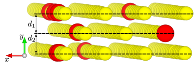
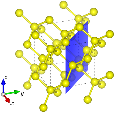
The principle of producing periodically bent crystals through doping is as follows: A dopant element, with a crystalline lattice constant slightly different from that of the base crystal, is introduced into the base crystal. This mismatch between lattice constants will produce a strain within the crystal, causing a change in the separation between neighbouring crystalline planes, leading to the bending of crystallographic planes [25]. When the dopant element has a larger lattice constant than the base crystal, it leads to an increase of the inter-planar distance. Conversely, a smaller lattice constant causes a decrease in the inter-planar distance. Figure 1 shows a portion of a Si crystal doped with Ge atoms, and highlights the planes within the crystalline structure and their respective inter-planar distances and . These inter-planar distances will depend on the concentration of dopant atoms within each plane. By increasing the concentration of dopant atoms, for example, along the crystal plane, the inter-planar distance is also systematically increased along this plane. Consequently, this will result in crystal bending along the plane. Figure 2 shows a single Si unit cell, highlighting the plane. Figures 1 and 2 in Breese [26], and Figure 4 in Krause et al. [25] illustrate this bending mechanism. If, at a certain stage, the dopant concentration is intentionally reduced in a systematic manner, the inter-planar distances would likewise decrease, resulting in the formation of a periodically bent structure.
In practice, doped crystals can be fabricated via a number of methods, including diffusion [27], ion implantation [28], chemical vapour deposition (CVD) [29, 30, 31, 32], and molecular beam epitaxy (MBE) [33], with each technique suited to growing different types of crystals. By selecting appropriate atom types and dopant concentrations, periodically bent crystals can be produced. In the case of gamma-ray CLSs, two crystal types have garnered significant research attention: Silicon crystals doped with Germanium (Si1-xGex), grown through MBE [33], and Diamond crystals doped with Boron (C1-xBx), grown via CVD [30]. Here, denotes the dopant concentration, where represents the base crystal with no dopant atoms, and denotes a single crystal of the dopant atom.
The dopant concentration can significantly influence the quality of the grown crystal. As dopant atoms are introduced, they induce strain within the crystal, leading to local changes in crystalline structure. These alterations, when considered across the entire crystal, lead to variation in the distances between neighbouring planes. However, if these distances become too large, various types of defects can emerge within the crystalline structure, including point defects and dislocations [34]. This outcome is dependent on the constituent atoms and the dopant concentration. For example, C1-xBx crystals have been shown to achieve higher dopant concentrations before defects begin to appear [35, 31]. In order to successfully manufacture high quality crystals, it is imperative that the maximum dopant concentration is kept below a critical value [25].
Herein, we report the results of an atomisitic-level study of the effect of dopant concentration and temperature on defect-free Si1-xGex crystals, and specifically how these parameters influence the crystalline properties of inter-planar distance and lattice constant. Our investigation employs molecular dynamics (MD) simulations using the MBN Explorer [36] and MBN Studio [37] software packages, allowing for the unique study of the direct effect of dopant atoms on the overall crystalline structure. This analysis holds significant relevance for the design and practical realisation of gamma-ray CLSs. To ensure the successful production of linear, bent, and periodically bent crystals suitable for use in CLSs, it is essential to identify the manufacturing tolerances of crystal properties. These include the maximum dopant concentration, bending amplitude, bending period, and minimum defect density for which effective channelling is still possible. In this study we focus on the dopant concentration, and the direct impact of dopant atoms on the small-scale crystalline structure.
2 Methodology
This section outlines the computational methodology used to generate defect-free doped Si1-xGex crystals, and their subsequent atomistic-level analysis. We considered a fixed crystal size of , comprising a total of 66,420 atoms. Our simulations were conducted under non-periodic boundary conditions at two distinct temperatures: and . These simulations have been performed using the MBN Explorer software package [36] for advanced multi-scale modelling of complex molecular structures and dynamics. MBN Studio [37], a multi-task toolkit and a dedicated graphical user interface for MBN Explorer, was utilised to construct the systems, prepare input files, and analyse simulation outputs.
Our investigation examines Si crystals doped with Ge at various concentrations to elucidate their influence on the crystalline structure. Due to the lattice mismatch between Si () and Ge () [38], Ge doping in Si causes an increase in the inter-planar distance. To generate the Si crystals, the MBN Explorer input file was configured with a single Si unit cell. This cell was then systematically duplicated and translated along each axis by the width of one Si lattice constant. This process was repeated until the entire volume of the simulation box was uniformly filled with the crystal structure. Subsequently, a predetermined percentage of Si atoms were selected at random and replaced with Ge atoms, ensuring the amount of Ge atoms aligned with the targeted dopant concentration: between (0%) and (15%). This method initially produces pristine crystalline structures devoid of defects, in comparison to techniques such as MBE and CVD. Although it is feasible to simulate MBE processes through MD calculations [39], such approaches are computationally expensive and beyond the scope of this study. We abstained from incorporating any form of substrate typical of MBE procedures [33], and restricted our examination to a single dopant concentration for each instance. Consequently, the crystals produced in our simulations do not exhibit the distinctive curvature or periodic distortion that are characteristic of periodically bent crystals produced with a gradient in dopant concentration. Subsequent studies will consider these factors in more detail.
The interactions between atoms within the crystals were simulated using the StillingerWeber potential [40]. The specific parameters for this potential, along with the atoms involved in these interactions, are summarised in Table 1(b).
| Constants | () | () | |||||
|---|---|---|---|---|---|---|---|
| 7.05 | SiSi | 2.095 | SiSiSi | 2.167 | SiSiSi | 21.0 | |
| 0.602 | SiGe | 2.138 | SiSiGe | 2.104 | SiSiGe | 23.1 | |
| 4.0 | GeGe | 2.181 | SiGeGe | 2.043 | SiGeGe | 25.5 | |
| 0.0 | GeSiSi | 2.043 | GeSiSi | 25.5 | |||
| 1.8 | GeSiGe | 1.984 | GeSiGe | 28.1 | |||
| 1.2 | GeGeGe | 1.926 | GeGeGe | 31.0 | |||
For each dopant concentration, independent crystalline structures were generated, ensuring a robust and statistically meaningful analysis. These geometries were optimised using the MBN Explorer velocity quenching algorithm over 10000 optimisation steps, and using a simulation box equal to the size of the crystal. From this optimised pool, 50 systems were then randomly selected for MD simulations. Each of these systems were heated to and using a Langevin thermostat with damping time of over a period of , to allow for thermalisation of the system. To accommodate the expected crystal expansion from atomic rearrangement, the simulation box dimensions were increased to .
For our analysis, we used the last 20 frames of the MD simulations, which represent the state of the systems over the concluding . During this period, we averaged the positions of the atoms in these frames to obtain crystal structures that account for thermal vibrations. To consider the bulk properties of the crystals, we deliberately excluded the edges from our analysis due to their atypical geometry, a consequence of non-periodic boundary interactions in the simulation box. We established a margin of from each edge of the crystal as the exclusion zone. This specific dimension was chosen as an optimal compromise, minimising the impact of edge artefacts while maximising the core crystal volume available for analysis.
3 Results and Discussion
As outlined in Section 1, the creation of periodically bent Si1-xGex crystals is dependent on the change in crystalline inter-planar distances by dopant Ge atoms. By analysing the relationship between the crystalline inter-planar distance and the dopant concentration on an atomistic scale, it is possible to evaluate the range of dopant concentrations for which high-quality, defect-free crystals can be grown. The crystals considered in this study are too small to exhibit the large-scale defect formation that would lead to dechannelling, thus the following analysis is considered from the viewpoint of the direct effect of dopant atoms on the spacing of crystalline planes.
The simulations conducted in this study allow for an atomistic-level investigation into the change in lattice constant and inter-planar distance from the nominal values of and , respectively, for single Si crystal. In order to determine the inter-planar distances within each crystal, atoms that lie along the (1 1 0) planes are identified and grouped into their respective planes. A set of coordinates that define the position of each plane relative to all neighbouring planes are then defined by taking the average coordinates in the (1 1 0) planes. From this, the distance between each neighbouring plane within the crystal is determined. The inter-planar distance is then averaged over all crystalline planes, and over all simulations for a particular dopant concentration.
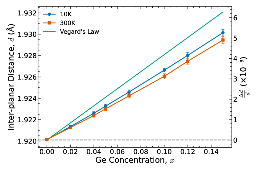
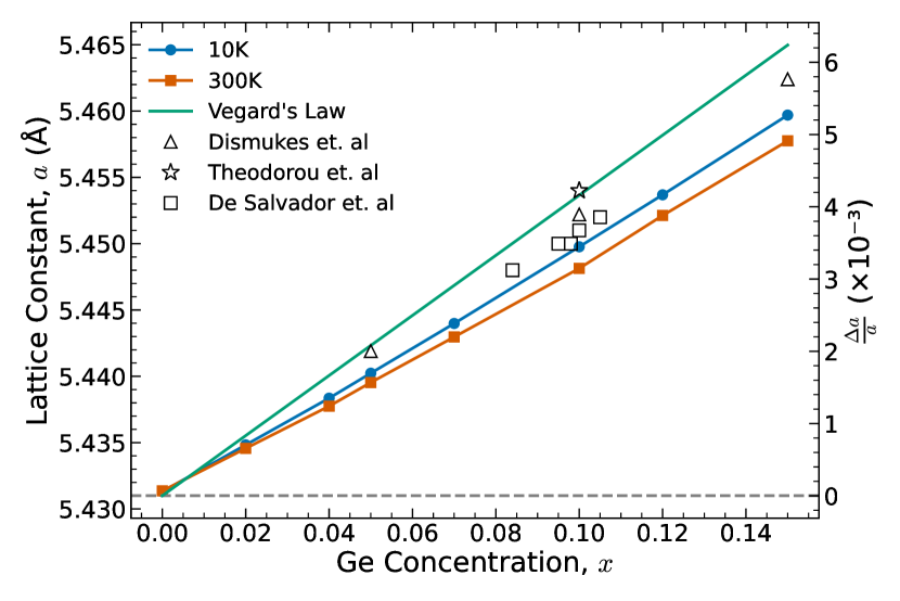
Figures 3(a) and 3(b) show how the average inter-planar distance and lattice constant vary with dopant concentration in comparison to the nominal parameters in single Si crystal. In addition, each plot has a second axis that shows the relative change in lattice constant or inter-planar distance , parameters commonly used in the manufacture of crystals [31, 30]. In both plots we observe an overall linear dependence on inter-planar distance and lattice constant with dopant concentration, with a dependence on temperature in the gradient. These results are compared to those of the empirically derived Vegard’s Law [44], predicting a linear proportionality between the lattice constant and the dopant concentration:
| (1) |
As the crystal scales in all directions, it follows that the inter-planar distance will adhere to the same relation: . The temperature will affect the gradient of this line, however for an accurate determination of this relation a systematic study over the range of expected operational temperatures ( - ) must be considered; this is beyond the scope of the current study. By conducting a linear fit of the form for each temperature, we can obtain a relationship comparable to Vegard’s Law, eq. 1. In the case of Figure 3(a), , and Figure 3(b), , equivalent to the nominal parameters for single Si crystals. The values of the gradient calculated for the inter-planar distance and the lattice constant are as follows:
| (2) | |||
| (3) |
Multiplying the values of by the ratio yields the values of , as expected. This decrease in gradient for increased temperature contradicts what one would expect from Vegard’s Law, with the lattice constant of Si corresponding to at . However, such a discrepancy is to be expected; it is well documented that Vegard’s Law (which was initially empirically derived) exhibits deviations from the results of both experimental and computational studies of the structure of semiconductor materials. Such deviations have been observed in diffraction experiments of Ge1-xSix [41, 45] and Ge1-xSnx [45], Monte Carlo simulations of Si1-xGex [42] and Ge1-xSix [46], MD simulations of Si1-xGex and Si1-xCx [47], and DFT simulations of Ge1-xSnx [48]. Jacob et al. [49] analyses Vegard’s Law in the frame of thermodynamics, stating that Vegard’s Law should be reclassified as an approximation. In particular, they specify that Vegard’s Law represents a valid approximation when the lattice constants of the components differ by less than 5%; in the case of Si and Ge, the lattice constants differ by %, thus Vegard’s Law provides a valid approximation for the change in lattice constant.
Discrepancies from Vegard’s Law are often accounted for by the modification of the linear interpolation to a parabolic relation
| (4) |
where the first two terms are the the linear relation eq. 1, and the final term accounts for the deviation from the linear behaviour, quantified by the bowing parameter . The values of have been obtained from a parabolic fit:
| (5) |
These values are larger compared to those obtained from other studies; from Dismukes et al. [41], from Theodorou et al. [42], and from Xu et al. [45]. Indeed, the deviation from Vegard’s Law we observe is slightly larger than that observed in other studies, seen in Figure 3(b). The physical explanation of this discrepancy likely originates in how the crystals used in this study have been generated. In our simulations, the crystals start with an ideal crystalline structure, regardless of the concentration of dopant atoms. The crystals are then allowed to relax as MD simulations are conducted, and the crystalline structure rearranges based on the dopant concentration. This is in contrast to crystals grown through MBE or CVD, which allows for the formation of dislocations and defects as the crystal is grown. Defects typically form over size ranges of nanometers [34], so it is not unexpected that our crystals show an ideal structure. In addition, our simulations neglect the substrates typically used for growth of crystals via MBE and CVD, and in combination with the non-peridoic nature of the simulation box, the crystals are allowed to scale in all directions, rather then just perpendicular to the substrate. This will impact the overall lattice constant.
4 Conclusions and Outlook
In this study, we have conducted atomistic-level simulations to examine the influence of dopant atoms on the structure of small Si1-xGex crystals, all within the context of emerging technologies for gamma-ray crystal-based light sources (CLSs). We have shown a linear relationship between dopant concentration and inter-planar distance and lattice constant between and . The system temperature affects the gradient of the linear relationship, with increased temperature resulting in a reduced lattice-constant. Our results show similar deviations from Vegard’s Law to Refs. [41, 45, 42, 46, 47, 48], but are in agreement with Vegard’s Law when it is considered as a general approximation, as outlined in Jacob et al. [49]. We observe an overall smaller lattice constant than Dismukes et al. [41] and [42]; however, we attribute this to our crystal generation method. Our crystals, being smaller and initially possessing an ideal structure, exhibit a much closer resemblance to an ideal crystal following MD simulations in comparison to the studies referenced. Their small size means large-scale defect formation is not possible, unlike crystals grown through conventional means. In addition, expansion of the crystal is not limited to a particular direction, as would be the case if a substrate were present.
This work has developed the basis for the simulation protocol for generating doped crystals in the context of gamma-ray CLSs. Future studies considering additional parameters, crystal types, and sizes will allow for the investigation of defect formation, as well as the influence of the substrate. The quality of crystals and understanding of defect forming processes are essential for the creation of gamma-ray CLSs. These simulations may be coupled with experimental studies to characterise the quality of candidate crystals, and channelling experiments run in parallel with relativistic MD [50] channelling simulations to evaluate the efficacy of radiation production of particular crystals. In the future more accurate crystal growth methods can be considered, such as MBE and CVD. These can be effectively explored using stochastic processes, such as Kinetic Monte Carlo simulations, which model the crystal growth through probabilistic processes [51]. This approach enables simulations over significantly longer timescales than traditional MD, making it comparable to MBE and CVD crystal growth. The recent successful integration of stochastic dynamics into MBN Explorer [52] has opened the door to further investigations into such stochastic processes.
This research field is inherently multidisciplinary, integrating simulation and experimental studies that are essential for the realisation of emerging gamma-ray CLSs.
Statements and declarations
Acknowledgments The authors acknowledge financial support from the European Commission’s Horizon Europe-EIC-Pathfinder-Open TECHNO-CLS (G.A. 101046458) project, from the H2020 RISE-NLIGHT project (G.A. 872196), and from the COST Action CA20129 MultIChem, supported by COST (European Cooperation in Science and Technology). The work was supported in part by Deutsche Forschungsgemeinschaft, Germany (Project No. 413220201). M. D. Dickers gratefully acknowledges receipt of a postgraduate studentship from UKRI. The possibility of performing computer simulations at the Goethe-HLR cluster of the Frankfurt Center for Scientific Computing is gratefully acknowledged. The authors thank A. V. Verkhovtsev for fruitful discussions.
Competing Interests The authors do not declare any conflicts of interest, and there is no financial interest to report.
Author Contribution MDD and AVK conducted the computational simulations and data analysis. MDD wrote the manuscript with support from AVK and input from all authors. GBS provided technical and computational advise and support for these simulations. NJM, FF, and AVS helped supervise the project and all authors provided critical feedback and helped shape the research and analysis.
Data Availability The datasets generated and/or analysed during the current study are available from the corresponding author upon reasonable request.
References
- \bibcommenthead
- Denker and Shklovsky [2013] Denker, B., Shklovsky, E.: Handbook of Solid-state Lasers: Materials, Systems and Applications. Woodhead Publishing, Cham (2013). https://doi.org/10.1533/9780857097507.2.171
- Ottaviano et al. [2012] Ottaviano, L., Semenova, E., Schubert, M., Yvind, K., Armaroli, A., Bellanca, G., Trillo, S., Nguyen, T.N., Gay, M., Bramerie, L., Simon, J.-C.: High-speed photodetectors in a photonic crystal platform. In: 2012 Conference on Lasers and Electro-Optics (CLEO), pp. 1–2 (2012). https://doi.org/10.1364/CLEO_SI.2012.CM1A.2
- Shkir et al. [2019] Shkir, M., Khan, M.T., Ashraf, I.M., Almohammedi, A., Dieguez, E., AlFaify, S.: High-performance visible light photodetectors based on inorganic CZT and InCZT single crystals. Sci. Rep. 9(1), 12436 (2019) https://doi.org/10.1038/s41598-019-48621-3
- Jethwa et al. [2021] Jethwa, V.P., Patel, K., Pathak, V.M., Solanki, G.K.: Enhanced electrical and optoelectronic performance of SnS crystal by Se doping. J. Alloys Compd. 883, 160941 (2021) https://doi.org/10.1016/j.jallcom.2021.160941
- Korol and Solov’yov [2022] Korol, A., Solov’yov, A.V.: Novel Lights Sources Beyond Free Electron Lasers. Springer, Cham (2022). https://doi.org/10.1007/978-3-031-04282-9
- Korol and Solov’yov [2020] Korol, A.V., Solov’yov, A.V.: Crystal-based Intensive Gamma-ray Light Sources. Europ. Phys. J. D. 74(10), 201 (2020) https://doi.org/10.1140/epjd/e2020-10239-8
- Korol and Solov’yov [2023] Korol, A.V., Solov’yov, A.V.: Atomistic Modeling and Characterizaion of Light Sources Based on Small-amplitude Short-period Periodically Bent Crystals. Nucl. Instrum. Meth. B 537, 1–13 (2023) https://doi.org/10.1016/j.nimb.2023.01.012
- Korol et al. [2014] Korol, A.V., Solov’yov, A.V., Greiner, W.: Channeling and Radiation in Periodically Bent Crystals. Springer, Heidelberg (2014). https://doi.org/10.1007/978-3-642-54933-5
- Sushko et al. [2022] Sushko, G.B., Korol, A.V., Solov’yov, A.V.: Extremely Brilliant Crystal-based Light Sources. Europ. Phys. J. D. 76(9), 166 (2022) https://doi.org/10.1140/epjd/s10053-022-00502-7
- Lindhard [1965] Lindhard, J.: Influence Of Crystal Lattice On Motion Of Energetic Charged Particles. Kongel. Dan. Vidensk. Selsk., Mat.-Fys. Medd. 34(14), 1–64 (1965)
- Momma and Izumi [2011] Momma, K., Izumi, F.: VESTA3 for three-dimensional visualization of crystal, volumetric and morphology data. J. Appl. Crystallogr. 44(6), 1272–1276 (2011) https://doi.org/10.1107/S0021889811038970
- Korol et al. [1999] Korol, A.V., Solov’yov, A.V., Greiner, W.: Photon Emission by an Ultra-relativistic Particle Channeling in a Periodically Bent Crystal. Int. J. Mod. Phys. E 08(01), 49–100 (1999) https://doi.org/10.1142/S0218301399000069
- Kumakhov [1976] Kumakhov, M.A.: On the Theory of Electromagnetic Radiation of Charged Particles in a Crystal. Phys. Lett. A 57(1), 17–18 (1976) https://doi.org/10.1016/0375-9601(76)90438-2
- Guidi et al. [2011] Guidi, V., Lanzoni, L., Mazzolari, A.: Patterning and Modeling of Mechanically Bent Silicon Plates Deformed through Coactive Stresses. Thin Solid Films 520(3), 1074–1079 (2011) https://doi.org/10.1016/j.tsf.2011.09.008
- Guidi et al. [2007] Guidi, V., Lanzoni, L., Mazzolari, A., Martinelli, G., Tralli, A.: Design of a Crystalline Undulator Based on Patterning by Tensile Si3N4 Strips on a Si Crystal. Appl. Phys. Lett. 90(11), 114107 (2007) https://doi.org/10.1063/1.2712510
- Guidi et al. [2005] Guidi, V., Antonini, A., Baricordi, S., Logallo, F., Malagù, C., Milan, E., Ronzoni, A., Stefancich, M., Martinelli, G., Vomiero, A.: Tailoring of Silicon Crystals for Relativistic-particle Channeling. Nucl. Instrum. Meth. B 234(1), 40–46 (2005) https://doi.org/%****␣sn-article.bbl␣Line␣300␣****10.1016/j.nimb.2005.01.008
- Bellucci et al. [2003] Bellucci, S., Bini, S., Biryukov, V.M., Chesnokov, Y.A., Dabagov, S., Giannini, G., Guidi, V., Ivanov, Y.M., Kotov, V.I., Maisheev, V.A., Malagù, C., Martinelli, G., Petrunin, A.A., Skorobogatov, V.V., Stefancich, M., Vincenzi, D.: Experimental Study for the Feasibility of a Crystalline Undulator. Phys. Rev. Lett. 90(3), 034801 (2003) https://doi.org/10.1103/PhysRevLett.90.034801
- Balling et al. [2009] Balling, P., Esberg, J., Kirsebom, K., Le, D.Q.S., Uggerhøj, U.I., Connell, S.H., Härtwig, J., Masiello, F., Rommeveaux, A.: Bending Diamonds by Femtosecond Laser Ablation. Nucl. Instrum. Meth. B 267(17), 2952–2957 (2009) https://doi.org/10.1016/j.nimb.2009.06.109
- Korol et al. [1998] Korol, A.V., Solov’yov, A.V., Greiner, W.: Coherent Radiation of an Ultrarelativistic Charged Particle Channelled in a Periodically Bent Crystal. J. Phys. G 24(5), 45 (1998) https://doi.org/10.1088/0954-3899/24/5/001
- Wagner et al. [2011] Wagner, W., Azadegan, B., Buettig, H., Grigoryan, L.S., Mkrtchyan, A., Pawelke, J.: Channeling Radiation on Quartz Stimulated by Acoustic Waves. Nuovo Cimento C 34(4), 133–140 (2011) https://doi.org/10.1393/ncc/i2011-10899-4
- Dedkov [1994] Dedkov, G.V.: Channeling Radiation in a Crystal Undergoing an Action of Ultrasonic or Electromagnetic Waves. Phys. Stat. Sol. 184(2), 535–542 (1994) https://doi.org/10.1002/pssb.2221840227
- Ikezi et al. [1984] Ikezi, H., Lin-Liu, Y., Ohkawa, T.: Channeling Radiation in a Periodically Distorted Crystal. Phys. Rev. B 30(3), 1567–1569 (1984) https://doi.org/10.1103/PhysRevB.30.1567
- Mikkelsen and Uggerhøj [2000] Mikkelsen, U., Uggerhøj, E.: A Crystalline Undulator Based on Graded Composition Strained Layers in a Superlattice. Nucl. Instrum. Meth. B 160(3), 435–439 (2000) https://doi.org/10.1016/S0168-583X(99)00637-0
- Romagnoni et al. [2022] Romagnoni, M., Guidi, V., Bandiera, L., De Salvador, D., Mazzolari, A., Sgarbossa, F., Soldani, M., Sytov, A., Tamisari, M.: Bent Crystal Design and Characterization for High-Energy Physics Experiments. Crystals 12(9), 1263 (2022) https://doi.org/10.3390/cryst12091263
- Krause et al. [2002] Krause, W., Korol, A.V., Solov’yov, A.V., Greiner, W.: Photon Emission by Ultra-relativistic Positrons in Crystalline Undulators: The High-energy Regime. Nucl. Instrum. Meth. A 483(1), 455–460 (2002) https://doi.org/10.1016/S0168-9002(02)00361-3
- Breese [1997] Breese, M.B.H.: Beam Bending using Graded Composition Strained Layers. Nucl. Instrum. Meth. B 132(3), 540–547 (1997) https://doi.org/10.1016/S0168-583X(97)00455-2
- Vlaskin et al. [2013] Vlaskin, V.A., Barrows, C.J., Erickson, C.S., Gamelin, D.R.: Nanocrystal Diffusion Doping. J. Am. Chem. Soc. 135(38), 14380–14389 (2013) https://doi.org/10.1021/ja4072207
- Poate and Saadatmand [2002] Poate, J.M., Saadatmand, K.: Ion beam technologies in the semiconductor world (plenary). Rev. Sci. Instrum. 73(2), 868–872 (2002) https://doi.org/10.1063/1.1428782
- Kaner et al. [1987] Kaner, R.B., Kouvetakis, J., Warble, C.E., Sattler, M.L., Bartlett, N.: Boron-carbon-nitrogen materials of graphite-like structure. Mater. Res. Bull. 22(3), 399–404 (1987) https://doi.org/10.1016/0025-5408(87)90058-4
- Connell et al. [2015] Connell, S.H., Härtwig, J., Masvaure, A., Mavunda, D., Tran Thi, T.N.: Towards a crystal undulator. In: Engelbrecht, C., Karataglidis, S. (eds.) Proceedings of the 59th Annual Conference of the South African Institute of Physics (SAIP2014), pp. 169–174. University of Johannesburg, Johannesburg (2015). https://events.saip.org.za/event/34/attachments/1143/1398/SAIP2014-169.pdf
- Brunet et al. [1998] Brunet, F., Germi, P., Pernet, M., Deneuville, A., Gheeraert, E., Laugier, F., Burdin, M., Rolland, G.: The effect of boron doping on the lattice parameter of homoepitaxial diamond films. Diam. Relat. Mater. 7(6), 869–873 (1998) https://doi.org/10.1016/S0925-9635(97)00316-6
- Wojewoda et al. [2008] Wojewoda, T., Achatz, P., Ortéga, L., Omnès, F., Marcenat, C., Bourgeois, E., Blase, X., Jomard, F., Bustarret, E.: Doping-induced anisotropic lattice strain in homoepitaxial heavily boron-doped diamond. Diam. Relat. Mater. 17(7), 1302–1306 (2008) https://doi.org/10.1016/j.diamond.2008.01.040 . Proceedings of Diamond 2007, the 18 European Conference on Diamond, Diamond-Like Materials, Carbon Nanotubes, Nitrides and Silicon Carbide
- Sakai [2011] Sakai, A.: 5 - Silicon–germanium (SiGe) Crystal Growth using Molecular Beam Epitaxy. In: Shiraki, Y., Usami, N. (eds.) Silicon–Germanium (SiGe) Nanostructures. Woodhead Publishing Series in Electronic and Optical Materials, pp. 83–116. Woodhead Publishing, Cham (2011). https://doi.org/10.1533/9780857091420.2.83
- Böer and Pohl [2020] Böer, K.W., Pohl, U.W.: Crystal Defects, pp. 1–54. Springer, Cham (2020). https://doi.org/10.1007/978-3-319-06540-3_15-4
- Tran Thi et al. [2017] Tran Thi, T.N., Morse, J., Caliste, D., Fernandez, B., Eon, D., Härtwig, J., Barbay, C., Mer-Calfati, C., Tranchant, N., Arnault, J.C., Lafford, T.A., Baruchel, J.: Synchrotron Bragg Diffraction Imaging Characterization of Synthetic Diamond Crystals for Optical and Electronic Power Device Applications. J. Appl. Crystallography 50(2), 561–569 (2017) https://doi.org/10.1107/S1600576717003831
- Solov’yov et al. [2012] Solov’yov, I.A., Yakubovich, A.V., Nikolaev, P.V., Volkovets, I., Solov’yov, A.V.: MesoBioNano Explorer–a Universal Program for Multiscale Computer Simulations of Complex Molecular Structure and Dynamics. J. Comput. Chem. 33(30), 2412–2439 (2012) https://doi.org/10.1002/jcc.23086
- Sushko et al. [2019] Sushko, G.B., Solov’yov, I.A., Solov’yov, A.V.: Modeling MesoBioNano Systems with MBN Studio Made Easy. J. Mol. Graph. Model. 88, 247–260 (2019) https://doi.org/10.1016/j.jmgm.2019.02.003
- Gražulis et al. [2009] Gražulis, S., Chateigner, D., Downs, R.T., Yokochi, A.F.T., Quirós, M., Lutterotti, L., Manakova, E., Butkus, J., Moeck, P., Le Bail, A.: Crystallography Open Database – an open-access collection of crystal structures. J. Appl. Crystallogr. 42(4), 726–729 (2009) https://doi.org/10.1107/S0021889809016690
- Ethier and Lewis [1992] Ethier, S., Lewis, L.J.: Epitaxial Growth of Si1-xGex on Si(100)2 × 1: A Molecular-Dynamics Study. J. Mat. Res. 7(10), 2817–2827 (1992) https://doi.org/10.1557/JMR.1992.2817
- Stillinger and Weber [1985] Stillinger, F.H., Weber, T.A.: Computer Simulation of Local Order in Condensed Phases of Silicon. Phys. Rev. B 31(8), 5262–5271 (1985) https://doi.org/10.1103/PhysRevB.31.5262 . Erratum: Phys. Rev. B 33(2), 1451 (1986) https://doi.org/10.1103/PhysRevB.33.1451
- Dismukes et al. [1964] Dismukes, J.P., Ekstrom, L., Paff, R.J.: Lattice Parameter and Density in Germanium-Silicon Alloys. J. Phys. Chem. 68(10), 3021–3027 (1964) https://doi.org/10.1021/j100792a049
- Theodorou et al. [1994] Theodorou, G., Kelires, P.C., Tserbak, C.: Structural, electronic, and optical properties of strained alloys. Phys. Rev. B 50(24), 18355–18359 (1994) https://doi.org/10.1103/PhysRevB.50.18355
- De Salvador et al. [2000] De Salvador, D., Petrovich, M., Berti, M., Romanato, F., Napolitani, E., Drigo, A., Stangl, J., Zerlauth, S., Mühlberger, M., Schäffler, F., Bauer, G., Kelires, P.C.: Lattice parameter of alloys. Phys. Rev. B 61(19), 13005–13013 (2000) https://doi.org/10.1103/PhysRevB.61.13005
- Vegard [1921] Vegard, L.: Die Konstitution der Mischkristalle und die Raumfüllung der Atome. Zeitschrift für Physik 5(1), 17–26 (1921) https://doi.org/10.1007/BF01349680
- Xu et al. [2017] Xu, C., Senaratne, C.L., Culbertson, R.J., Kouvetakis, J., Menéndez, J.: Deviations from Vegard’s law in semiconductor thin films measured with X-ray diffraction and Rutherford backscattering: The Ge1-ySny and Ge1-xSix cases. J. Appl. Phys. 122(12), 125702 (2017) https://doi.org/10.1063/1.4996306
- de Gironcoli et al. [1991] Gironcoli, S., Giannozzi, P., Baroni, S.: Structure and thermodynamics of alloys from ab initio Monte Carlo simulations. Phys. Rev. Lett. 66(16), 2116–2119 (1991) https://doi.org/10.1103/PhysRevLett.66.2116
- Tersoff [1989] Tersoff, J.: Modeling solid-state chemistry: Interatomic potentials for multicomponent systems. Phys. Rev. B 39(8), 5566–5568 (1989) https://doi.org/10.1103/PhysRevB.39.5566
- Chizmeshya et al. [2003] Chizmeshya, A.V.G., Bauer, M.R., Kouvetakis, J.: Experimental and Theoretical Study of Deviations from Vegard’s Law in the SnxGe1-x System. Chem. Mert. 15(13), 2511–2519 (2003) https://doi.org/10.1021/cm0300011
- Jacob et al. [2007] Jacob, K.T., Raj, S., Rannesh, L.: Vegard’s law: a fundamental relation or an approximation? Int. J. of Mater. Res. 98(9), 776–779 (2007) https://doi.org/10.3139/146.101545
- Sushko et al. [2013] Sushko, G.B., Bezchastnov, V.G., Solov’yov, I.A., Korol, A.V., Greiner, W., Solov’yov, A.V.: Simulation of Ultra-relativistic Electrons and Positrons Channeling in Crystals with MBN Explorer. J. Comput. Phys. 252, 404–418 (2013) https://doi.org/10.1016/j.jcp.2013.06.028
- Voigtländer [2001] Voigtländer, B.: Fundamental processes in Si/Si and Ge/Si epitaxy studied by scanning tunneling microscopy during growth. Surf. Sci. Rep. 43(5), 127–254 (2001) https://doi.org/10.1016/S0167-5729(01)00012-7
- Solov’yov et al. [2022] Solov’yov, I.A., Sushko, G., Friis, I., Solov’yov, A.V.: Multiscale modeling of stochastic dynamics processes with MBN Explorer. J. Comput. Chem. 43(21), 1442–1458 (2022) https://doi.org/10.1002/JCC.26948