Non-utopian optical properties computed of a tomographically reconstructed real photonic band gap crystal
††journal: opticajournal††articletype: Research ArticlesOm\IfBooleanTF#1 \dgalext#3 \dgalx[#2]#3 \NewDocumentCommand\dgalextm{{#1}} \NewDocumentCommand\dgalxom{{#2}} \tikzsetfigurenamephysics-real-crystal-figure \tikzexternalize\tikzsetexternalprefixfigurecache/ \tikzsetevery picture/.style=ultra thick
https://nano-cops.com
State-of-the-art computational methods combined with common idealized structural models provide an incomplete understanding of experimental observations on real nanostructures, since manufacturing introduces unavoidable deviations from the design. We propose to close this knowledge gap by using the real structure of a manufactured crystal as input in computations to obtain a realistic comparison with measurements on the same nanostructure. We demonstrate this approach on the structure of a real inverse woodpile photonic bandgap crystal made from silicon, as previously obtained by synchrotron X-ray imaging. A 2D part of the dataset is selected and processed into a computational mesh suitable for a Discontinuous Galerkin Finite Element Method (DGFEM) to compute broadband optical transmission. We compare this to the transmission of a utopian crystal: a hypothetical model crystal with the same filling fraction where all pores are taken to be identical and circular. The shapes of the nanopores in the real crystal differ in a complex way from utopian pores due to scallops, tapering, or roughness. Hence, the transmission spectrum is complex with significant frequency speckle both outside and inside the main gap. The utopian model provides only limited understanding of the spectrum: while it accurately predicts low frequency finite-size fringes and the lower band edge, the upper band edge is off, it completely misses the presence of speckle, the domination of speckle above the gap, and possible Anderson localized states in the gap. Moreover, unlike experiments where one can only probe from the outside of a real crystal, the use of a numerical method allows us to study all fields everywhere. While at low frequencies the effect of the pore shapes is minimal on the fields, major differences occur at higher frequencies including the gap such as high-field states localized deep inside the real crystal. We conclude that using only external measurements and utopian models may give an erroneous picture of the fields and the local density of states (LDOS) inside a real crystal, while this is remedied by our new approach.
1 Introduction
The field of nanophotonics promises control over emission and propagation of light by tailoring the environment [1, 2, 3]. Photonic crystals are a particularly promising tool for the goal of simultaneous control of light in all three dimensions (3D). Such photonic crystals are defined by a periodic variation of the refractive index commensurate with optical wavelengths, which results in photonic dispersion relations organized in bands, analogous to the electron bands in solids [4, 5]. Analogous to the electronic band gap, there is a complete 3D photonic band gap, a frequency gap without any bands. Within the 3D band gap, no light modes exist inside the crystal, hence the density of states (DOS) strictly vanishes. In finite crystals, the local density of states does not vanish completely, but by making the crystal large enough it can be suppressed to arbitrarily low levels [6, 7, 8]. A 3D gap is therefore a powerful tool to radically control the spontaneous emission and cavity quantum electrodynamics (QED) of embedded quantum emitters [9, 10]. There is a wide range of applications of 3D photonic band gap crystals, including efficient photovoltaic cells [11, 12], miniature lasers [13], thermal emission control [14, 15], mode and polarization converters [16], cloaking devices [17], and 3D photonic integrated circuits [18, 19].
Inevitably, every fabricated 3D photonic crystal will, like any nanostructure, deviate from its design, both systematically in the form of structural deformations and statistically in shape and size variations. Consequently, the optical properties of actual samples differ from those of the design [20, 21, 22]. Testing the optical properties of a real sample, for example by measuring a stopband in reflection, typically shows a complex signal that differs markedly from theoretical predictions [23]. These differences could not only be caused by the manufacturing deviations, but also by the experiment or the model that was used to predict the optical properties in the first place. To guide design, experiment, and modeling of nanophotonic devices, it is thus crucial to understand how real devices with manufacturing deviations differ from the perfect devices that could only be manufactured in a utopian cleanroom. Here we propose and demonstrate a completely new approach to nanophotonics to bridge the gap between model and experiment.
2 Interpreting experiments with models
2.1 Traditional approach
To put our new approach in perspective, let us first discuss the limitations of the current traditional approach to nanophotonics. As with most physics research the traditional approach consists of two tracks: experiments and theory. The central idea is that if we can explain a set of experiments with a theory then we understand what is happening. In reality, this is quite difficult with large nanophotonic devices, because there are significant complications and limitations on both the experimental and the theoretical tracks.
To understand the limitations of the traditional approach, illustrated in Figure 1(a), we consider that we have a design for a large nanophotonic device, e.g., a 3D photonic band gap crystal, whose physical properties we seek to understand. The experimental route consists of two steps: The design is used to manufacture a number of samples, a beam with photonic crystals in our case. Each sample is then mounted into an experimental setup so that its optical properties are measured, for example, the reflectivity as function of frequency [23, 24]. The theoretical route consists of putting a model of the design into a computer for a computation using a numerical method like a Finite Element Method (FEM) [25], Plane Wave Expansion (PWE) [26], or Finite Difference Time Domain (FDTD) [27]. Which optical properties can be computed in this way depends on the model, but in theory they are expected to match the experimental results. In practice this is much more difficult, and with a complicated system like a photonic crystal one is happy with a limited match between theory and experiment, for example, the center frequency of a measured reflectivity peak at is the center of a theoretically predicted bandgap [28, 29].
at (-1.5,0) [rectangle,draw,align=center] (design)
Sample Design
Inverse Woodpile;
at (2,1.5) [rectangle,draw,align=center, minimum width=9em] (sample)
Sample
Crystal bar;
\nodeat (5,1.5) [rectangle,draw,align=center, minimum width=6em] (experiment)
Experiment
Reflection;
\nodeat (8,1.5) [rectangle,draw,align=center, minimum width=8.5em] (result)
Experimental Result
Spectra;
at (2,-1.5) [rectangle,draw,align=center] (model)
Model
(In)finite crystal;
\nodeat (5,-1.5) [rectangle,draw,align=center] (computation)
Computation
PWE, FEM;
\nodeat (8,-1.5) [rectangle,draw,align=center] (tresult)
Numerical Result
Band structure
Spectra;
[red] at (8,0) [align=center](comparison) Comparing “apples to oranges”;
[->,red] (design) to[out=90,in=180] node[label=[shift=(-1.8em,-0.25ex)]south east:Manufacturing](sample); \draw[->] (sample) – (experiment); \draw[->] (experiment) – (result);
[->,red] (design) to[out=270,in=180] node[label=[shift=(-2em,0.75ex)]north east:Model assumptions] (model); \draw[->] (model) – (computation); \draw[->] (computation) – (tresult);
[->] (result) – (comparison); \draw[->] (tresult) – (comparison);
at (-1.5,0) [rectangle,draw,align=center] (design)
Sample Design
Inverse Woodpile;
at (2,2) [rectangle,draw,align=center, minimum width=9em] (sample)
Sample
Crystal bar;
\nodeat (5,2) [rectangle,draw,align=center, minimum width=6em] (experiment)
Experiment
Reflection;
\nodeat (8,2) [rectangle,draw,align=center, minimum width=8.5em] (result)
Experimental result
Spectra;
at (2,0) [rectangle,draw,align=center, minimum width=9em] (structure)
Real structure
X-ray reconstruction;
\nodeat (5,0) [rectangle,draw,align=center, minimum width=6em] (simulation)
Computation
FDTD, FEM;
\nodeat (8,0) [rectangle,draw,align=center, minimum width=8.5em] (sresult)
Simulation Result
Spectra, fields;
at (2,-2) [rectangle,draw,align=center, minimum width=9em] (model)
Model
Finite crystal;
\nodeat (5,-2) [rectangle,draw,align=center, minimum width=6em] (computation)
Computation
FDTD, FEM;
\nodeat (8,-2) [rectangle,draw,align=center, minimum width=8.5em] (tresult)
Numerical Result
Spectra, fields;
[->,red] (design) to[out=90,in=180] node[below right]Manufacturing (sample); \draw[->] (sample) – (experiment); \draw[->] (experiment) – (result); \draw[->] (sample) to[] (structure); \draw[->] (structure) – (simulation); \draw[->] (simulation) – (sresult); \draw[->,red] (design) to[out=270,in=180] node[above right]Model assumptions (model); \draw[->] (model) – (computation); \draw[->] (computation) – (tresult);
[red] at (8,1) [align=center](comparison) Experimental insight; \draw[->] (result) – (comparison); \draw[->] (sresult) – (comparison);
[red] at (8,-1) [align=center](comparison2) Model comparison; \draw[->] (sresult) – (comparison2); \draw[->] (tresult) – (comparison2);
The source of these complications is in all three steps, (1) computation, (2) experiment and (3) manufacturing. We discuss the complications introduced by each of these steps individually.
(1) Computationally the challenges in essence revolve around the finite computer memory and computation time. A realistic simulation of the experimental situation is beyond the ability of current (super)computers for anything but the tiniest photonic crystals. Therefore, the computational approach has to make modelling assumptions and simplifications. Typical examples are simplifying an incident beam from focus to plane wave, using an infinite rather than finite crystal, or using only simple geometric shapes rather than a freeform structure. These assumptions affect the computed optical properties and thus limit and complicate a comparison with experiment. An extreme example of this is the use of an infinite crystal and the computation of a band structure. The lack of any external interface and finite size effects means that such a band structure is limited in what it can predict and explain about experiments.
(2) Challenges with the experiment are primarily practical, i.e., we need to get a reliable signal for the optical property that we want to measure. The extent and design of photonic crystals means that we are limited in what kind of signals we can obtain, as we can not “just stick a probe in there”, especially not in 3D nanostructures [30]. Even if we could, this probe would probably affect the optical properties under study. Moreover, not all effects give a significant signal, for example, measuring the effect of a bandgap through transmission is hard because the prediction is that there should be a vanishing transmission, but a vanishing signal could also be caused by a myriad of other reasons, and such a signal is thus potentially unobservable due to noise.
(3) The central challenge with manufacturing is that it will inevitably introduce deviations from the original design, thereby altering the optical properties [22, 31, 32]. The current techniques for manufacturing photonic crystals will leave artifacts, and these artifacts are large enough that they significantly impact device performance, as will be shown in our results. These artifacts can roughly be grouped into two categories, systematic and random. A systematic deviation is one where the whole crystal deviates from the design in a predictable manner, for example, the misalignment of two parts of the design [20, 33]. With random deviations the actual crystal deviates from the design in a way that can only be characterized statistically, for example, if the shape of each feature is deformed in a different way.
The current traditional approach to estimate and understand the effects of manufacturing deviations is to use computational and theoretical models. This is very useful for systematic manufacturing deviations, as one can typically model these with one or a few parameters, like an offset parameter to model a misalignment. Studying the effect of such a parameter is the same as optimizing any other design parameter like lattice constants and feature sizes [33]. There are three problems with this approach for predicting the effect of more random manufacturing deviations. Firstly, one needs to have a parameterized model to generate such deviations. But deviations like shape variations are very difficult to realistically model with a tractable number of parameters. Secondly, the randomness means that one needs a realistic probability distribution for the generation of these deviations, but there is typically no information about these distributions in a real crystal with a few rare exceptions [34]. Thirdly, the randomness means that the optical properties are only valid for one specific generated realization, which is not necessarily realistic [20]. One could work around this by using ensemble averaged properties [35]. However, such statistical quantities only give information about an ensemble of samples and are therefore unsuitable to explain what happens in a single sample with a specific configuration [22, 36].
2.2 Our data-driven approach
Our new data-driven approach tackles the problem of the unrealistic utopian structure used in the computations, as illustrated in Figure 1(b). We do this by extracting the crystal structure from a tomography reconstruction of a real crystal, thereby including all manufacturing details. This structure is then used for a computation of the optical properties of the photonic crystal. We envision two ways how our new approach can complement the current approaches.
(1) The comparison between measurements from a real crystal with the computation is based on the structure of the same crystal. By using the real structure of the crystal one includes the exact manufacturing deviations from the utopian design, just as in the experiment. The effect of these deviations should therefore be the same in both experiment and computation thereby obviating many assumptions, giving a more accurate comparison. Moreover, as we can study the field inside a crystal with a computation, we can effectively investigate effects that are difficult or even impossible to probe in an experiment.
(2) The comparison between computations with real structure and computations with related model geometries can be used to determine how accurate the model is as predictor for a real nanostructure. Optical properties that are both present in the model and the real-structure computation are likely relatively robust with respect to manufacturing deviations and thus also present in a real nanostructure. Properties of the model that are absent in the real-structure computation are likely sensitive to manufacturing deviations and thus not present in the real nanostructure.
The use of the structure of a real nanostructure in our approach is what makes these applications possible and what makes it fundamentally different from previous approaches with modeled manufacturing deviations. These previous modeled manufacturing deviations are limited by human imagination, which includes parametrizing them and finding a proper distribution for the randomness. The use of the structure of a real sample bypasses these problems as it uses the actual physical process to generate a real computational version of manufacturing deviations according to the actual statistical distribution. Moreover, because the reconstruction is of a real nanostructure, we are not limited to ensemble avaraged quantities, as the actual computed properties are relevant for that specific sample, and in terms of statistical physics: on that specific configuration [36].
3 Methods
3.1 Design and dataset
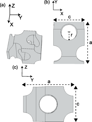
The unit cell design for the inverse woodpile photonic crystal structure is shown in Figure 2–2 [37]. The crystal structure consists of intersecting pores with radius along the and direction. The pores in the and directions form a centered rectangular lattice in the and planes, respectively. This crystal has lattice parameters and , with , such that the crystal has a face centred cubic (fcc) lattice, with a diamond like symmetry [37, 38].
In practice, real 3D photonic bandgap crystals are manufactured from silicon on the edge of a beam using methods described in Refs. [39, 40, 41]. In brief, a mask with an array of apertures is made on both the top and front sides of the beam, followed by two consecutive reactive ion etching steps to etch nanopores both from the top and the side of the Si beam. The volume where the two pore sets overlap is a 3D periodic nanostructure with the inverse woodpile structure.
c-0.5t0pt(2)
{tikzpicture}
\node[anchor=south west,inner sep=0] (image) at (0,0)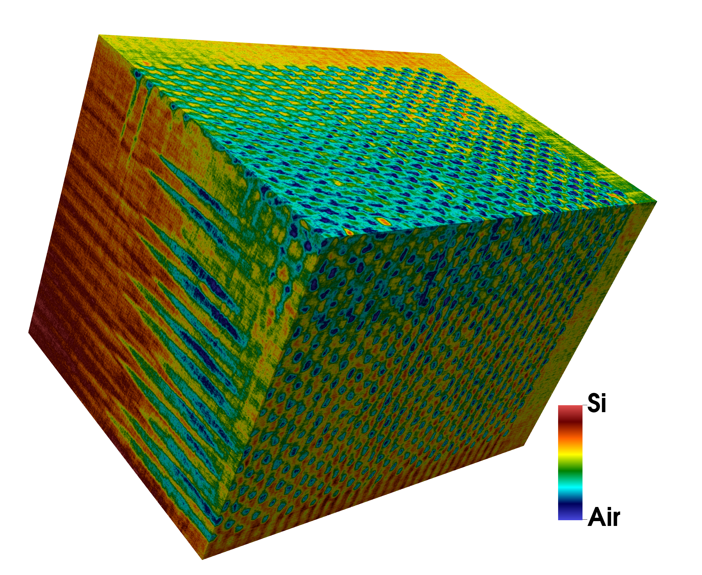 ;
{scope}[x=(image.south east),y=(image.north west)]
\draw[->] (93/2332,1-1109/1910) – (671/2332, 1-1860/1910) node[below]-X;
\draw[->] (93/2332,1-1109/1910) – (328/2332, 1-114/1910) node[above]Z;
\draw[->] (328/2332, 1-114/1910) – (1463/2332, 1-179/1910) node[right]-Y;
\draw[dashed] (432.6/2332, 1-1550.2/1910) – (764.2/2332,1-511.2/1910) – (1886/2332,1-466.9/1910);
;
{scope}[x=(image.south east),y=(image.north west)]
\draw[->] (93/2332,1-1109/1910) – (671/2332, 1-1860/1910) node[below]-X;
\draw[->] (93/2332,1-1109/1910) – (328/2332, 1-114/1910) node[above]Z;
\draw[->] (328/2332, 1-114/1910) – (1463/2332, 1-179/1910) node[right]-Y;
\draw[dashed] (432.6/2332, 1-1550.2/1910) – (764.2/2332,1-511.2/1910) – (1886/2332,1-466.9/1910);
l0ptt0pt\tikzsetexternal/export next=true{tikzpicture}
\node[fill=white,inner sep=1,outer sep=1] at (0,0) (2);
{tikzpicture}
\node[anchor=south west,inner sep=0] (image) at (0,0)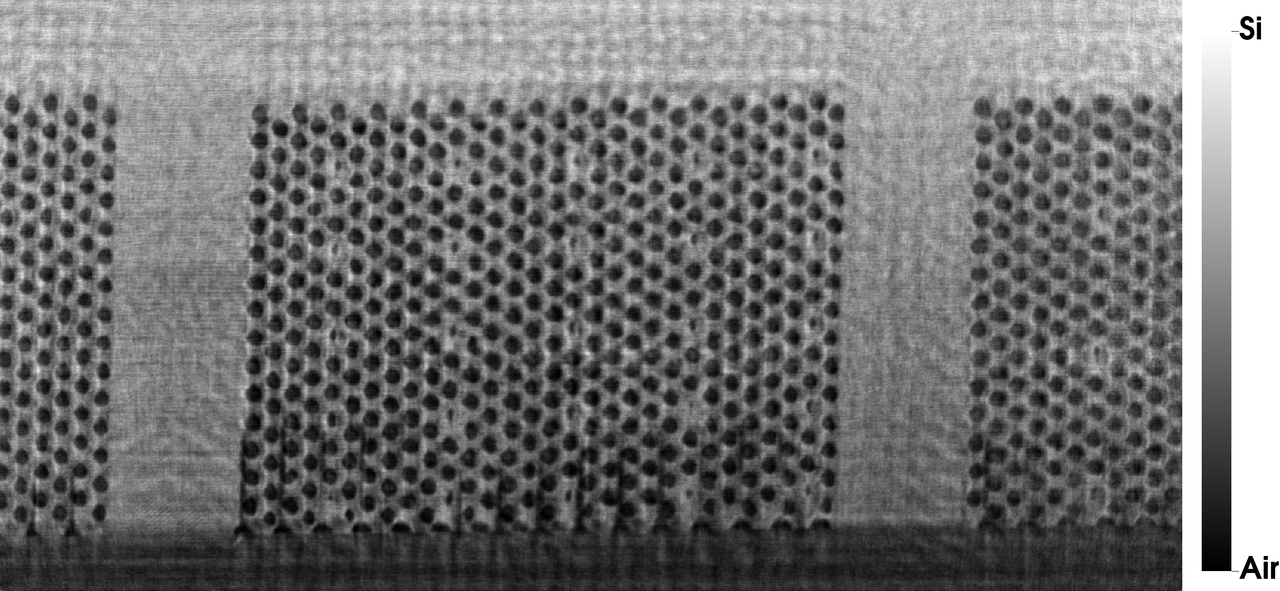 ;
{scope}[x=(image.south east),y=(image.north west)]
[white] (0.10,1) rectangle (0.195,0.775);
\draw[->,black] (0.11,0.95) – (0.11, 0.85) node[below]Z;
\draw[->,black] (0.11,0.95) – (0.16,0.95) node[right]Y;
\node[black,label=[black,label distance=-0.3cm]right:X] at (0.135,0.9) ;
;
{scope}[x=(image.south east),y=(image.north west)]
[white] (0.10,1) rectangle (0.195,0.775);
\draw[->,black] (0.11,0.95) – (0.11, 0.85) node[below]Z;
\draw[->,black] (0.11,0.95) – (0.16,0.95) node[right]Y;
\node[black,label=[black,label distance=-0.3cm]right:X] at (0.135,0.9) ;
A number of these crystals were non-destructively imaged using X-ray imaging (holotomography) [42, 29, 43, 44, 40]. Tomographic reconstruction was used to obtain the electron density inside the scanned volume. The resulting datasets are divided in cubic voxels, with each voxel associated with the electron density in its volume. We note that obtaining quantitative electron densities is a major step forward over the arbitrary units typical of scanning electron microscopy (SEM). From all datasets we choose the one with the smallest voxels and the largest contrast in electron density, expecting this will give the most accurate reconstruction. This specific dataset has cubic voxels with edges. The axes of this dataset are aligned to be parallel to the top and side plane of the beam with crystals. Moreover, since the pores extend perpendicular from the surface of the beam, this alignment results in pores that are also aligned with the dataset axes.
Figure 2 shows part of the dataset with size voxels that corresponds to 33% of the whole dataset. It highlights a single crystal on the silicon beam. The variations on the three image planes correspond to the intersection with the crystal pores. Periodic variations are apparent from intersections with the 2D lattices of pores. The lengthwise cross-section is visible on the plane, which also shows that the pores in the direction are less than a third of the length and thinner than those in the direction.
Figure 2 shows a complete slice of the dataset in the -plane at the edge of the silicon beam, approximately below the top surface. Three photonic crystals are visible, a complete one in the middle and two partial ones on the left and right. The transition between dark area at the bottom (vacuum) and lighter area is the front surface of the silicon beam.
The lattice of circular dark areas correspond to the intersection of this slice with the pores in the -direction. The periodic lighter pores in the middle and right crystal are pores with a reduced size in the design thereby creating a lattice of defects. The pores in the -direction are short and thin and as result barely visible.
From this slice we estimate that the deepest pores in the -direction are approximately lattice constants deep, corresponding to approximately . Thus there are only pores in both the and -directions in the volume near the -surface. The crystal volume that is deeper only has pores in the -direction, thus forming a quasi-2D structure, see also Ref. [40].
3.2 Data processing
Numerical computations on the total dataset volume with all voxels are at this time not feasible as they require prohibitively large computational resources. As a result it would, if at all possible, put such severe restrictions on spatial and frequency resolution that a comparison to experiment would not be meaningful. Therefore, for this study we limit ourselves to a part of the 2D-slice of Figure 2. The reason for choosing a part of a 2D-slice is that this reduces computational cost and allows high-resolution computations to accurately compute the field around the irregular pore shapes. While the 2D slice is not directly comparable to experiment, it does contain real manufacturing deviations and is thus interesting for quantifying the optical effects these manufacturing deviations have. The selected part is shown in Figure 3, which is the largest region in the dataset that is in the 2D part of a crystal with uniform pores in the design. The edge of the region is chosen to cut through the middle of pores to allow mirroring the domain along the edges. After this mirroring the pores on the edge of the domain have nearly the same size as the pores that are completely inside the domain.
l0ptt0pt\tikzsetexternal/export next=true{tikzpicture}
\node[fill=white,inner sep=1,outer sep=1] at (0,0) (3);
{tikzpicture}
\node[anchor=south west,inner sep=0] (image) at (0,0)
 ;
{scope}[x=(image.south east),y=(image.north west)]
\draw[red,ultra thick]
(1-24/800,1-52/210) –
(1-27.6/800,1-190/210) –
(1-641.6/800,1-174/210) –
(1-638/800,1-36/210) –
(1-24/800,1-52/210);
;
{scope}[x=(image.south east),y=(image.north west)]
\draw[red,ultra thick]
(1-24/800,1-52/210) –
(1-27.6/800,1-190/210) –
(1-641.6/800,1-174/210) –
(1-638/800,1-36/210) –
(1-24/800,1-52/210);
[white] (0.0, 0.0) rectangle (0.125,0.025 + 0.10*800/210); \draw[black,->] (0.025,0.05) – (0.075,0.05) node [right] -Z; \draw[black,->] (0.025,0.05) – (0.025,0.05 + 0.05*800/210) node [above] -Y; \node[black,label=[black,label distance=-0.3cm]right:X] at (0.05+0.025,0.025+0.05*800/210) ;
l0ptt0pt\tikzsetexternal/export next=true{tikzpicture}
\node[fill=white,inner sep=1,outer sep=1] at (0,0) (3);
{tikzpicture}[spy using outlines=rectangle, magnification=3,connect spies,
every spy on node/.append style=thick]
\node[anchor=south west,inner sep=0] (image) at (0,0)
 ;
{scope}[x=(image.south east),y=(image.north west)]
\coordinate(spypoint) at (0.20,0.24);
\coordinate(spyviewer) at (0.6,0.5);
\spy[width=4cm,height=2.4cm] on (spypoint) in node [fill=white] at (spyviewer);
[white] (0.01,0.7) rectangle (0.0907,0.8);
\node[black] at (0.05035,0.75) ;
[white] (0.0, 0.0) rectangle (0.125,0.025 + 0.10*1004/225);
\draw[black,->,ultra thick] (0.025,0.05) – (0.075,0.05) node [right] Y;
\draw[black,->,ultra thick] (0.025,0.05) – (0.025,0.05 + 0.05*1004/225) node [above] -X;
;
{scope}[x=(image.south east),y=(image.north west)]
\coordinate(spypoint) at (0.20,0.24);
\coordinate(spyviewer) at (0.6,0.5);
\spy[width=4cm,height=2.4cm] on (spypoint) in node [fill=white] at (spyviewer);
[white] (0.01,0.7) rectangle (0.0907,0.8);
\node[black] at (0.05035,0.75) ;
[white] (0.0, 0.0) rectangle (0.125,0.025 + 0.10*1004/225);
\draw[black,->,ultra thick] (0.025,0.05) – (0.075,0.05) node [right] Y;
\draw[black,->,ultra thick] (0.025,0.05) – (0.025,0.05 + 0.05*1004/225) node [above] -X;
l0ptt0pt\tikzsetexternal/export next=true{tikzpicture}
\node[fill=white,inner sep=1,outer sep=1] at (0,0) (3);
{tikzpicture}[spy using outlines=rectangle, thick, magnification=3,connect spies,
every spy on node/.append style=thick]
\node[anchor=south west,inner sep=0] (image) at (0,0) 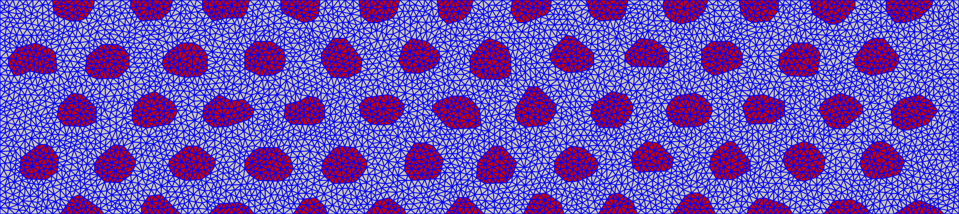 ;
{scope}[x=(image.south east),y=(image.north west)]
\coordinate(spypoint) at (0.20,0.24);
\coordinate(spyviewer) at (0.6,0.5);
\spy[width=4cm,height=2.4cm,thick] on (spypoint) in node [fill=white] at (spyviewer);
[white] (0.01,0.7) rectangle (0.0907,0.8);
\node[black] at (0.05035,0.75) ;
;
{scope}[x=(image.south east),y=(image.north west)]
\coordinate(spypoint) at (0.20,0.24);
\coordinate(spyviewer) at (0.6,0.5);
\spy[width=4cm,height=2.4cm,thick] on (spypoint) in node [fill=white] at (spyviewer);
[white] (0.01,0.7) rectangle (0.0907,0.8);
\node[black] at (0.05035,0.75) ;
The processing of the dataset to a mesh for a finite element computation consists of three steps: Cutting out the region, extracting the pore-silicon interface, and meshing. These three steps are automated using Nanomesh [45], an open source Python library for processing 2D and 3D data into computational meshes. The code for all these steps and the actual computation are available as part of the dataset in Ref. [46]
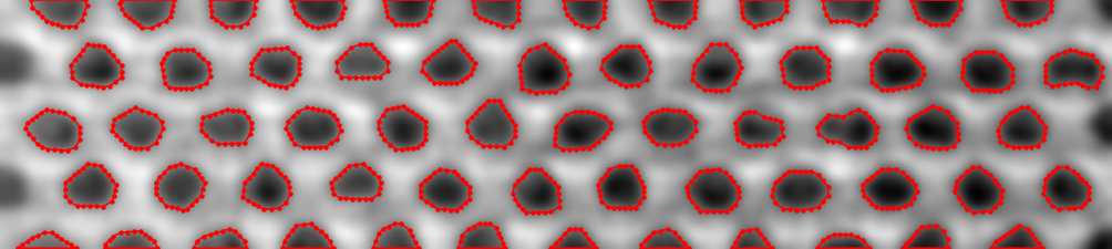
The slice in Figure 3 and the dataset in general shows high frequency noise and line artifacts. To reduce these artifacts the images are smoothed using a Gaussian filter with a standard deviation corresponding to pixels. This agrees well with the pixels spatial accuracy as determined in Ref. [29]. The smoothed image is segmented into two regions, air and silicon, using local thresholding [47, 48]. The region is determined by comparing each pixel to an offset plus a weighted mean of the surrounding square of pixels. This use of a local threshold is essential because there is an intensity gradient in the dataset. With a global threshold this gradient would introduce a gradient in the pore sizes. The size of the comparison region and the threshold were visually chosen to result in pore outlines that conform to the X-ray dataset. Lastly, the marching cubes algorithm [49] is used to convert the segmentation into a pore boundary.
Figure 3 shows the silicon-air interface of the pores overlayed on the dataset after applying the Gaussian filter. Based on the inverse woodpile design[37] of this sample we had expected the pores to be circles or ellipses. However, both the reconstructed contours and the X-ray data of Figure 3 shows that the pore shape and size varies significantly in the real crystal. Possible reasons for these deviations include unknown subtleties in the etching[50, 41], and image artifacts in the X-ray holotomography reconstruction [29]. Nevertheless, the resulting pore shapes have similar shapes as those seen in SEM images of the external surface of the same crystal, indicating that the reconstruction is realistic.
The interfaces of the partial pores on the left and right boundaries are discarded to create a flat crystal interface, similar to the interface of the actual inverse woodpile. The interface from the segmentation step is used to constrain the meshing algorithm to get a mesh that exactly follows this interface. An example of such a mesh is shown in Fig. 3, which is the coarsest mesh used to determine the accuracy of our results (see supplementary material). The transmission spectrum and fields presented here use triangles with about smaller edges, thus yielding accurate results.
3.3 Numerical
To compute the optical transmission of the reconstructed crystal we use a Discontinuous Galerkin Finite Element Method (DGFEM) to solve the time-harmonic Maxwell’s equations[51, 52, 53, 54, 25]. The details of the method can be found in the supplementary material, in short we use an Interior Penalty discretization for the time harmonic Maxwell’s equations using piecewise second order Nédélec elements. Combined with the mesh that resolves the interface we accurately handle the sharp contrast in the dielectric constant between silicon and air.
The computational setup is shown in Figure 4. The mesh obtained from X-ray image processing is extended by a layer of air on the left and silicon to the right. This is similar to the real crystal, which is on the edge of a silicon beam [39]. We take the relative permittivity of silicon as , matching with previous results [33, 55]. On the top and bottom we use perfectly conducting boundary conditions to create mirror symmetry. By using this on both boundaries we obtain half of a structure that extends periodically in the vertical direction. Alternatively, the two perfectly conducting boundaries can be interpreted as making the domain into a strip waveguide, the resulting effects are further discussed in section 5.2
We consider light with the magnetic field orthogonal to the computational plane, in photonic crystals known as TE polarization [1], and in waveguides as TM polarization[56]. As incident fields we send in a plane wave from the air region, with the electric field parallel to the air-crystal interface. This is the lowest order mode supported by the domain, denoted as the 0-th mode.
For the computation of the total electric field we use a scattering approach, where we consider the computational setup as an air-silicon interface with the air-pores as added scatterers. The total electric field is thus split into two parts , a background field from the interface and a field from the scattering by the pores. The background field consists of the incident plane wave and its reflection and transmission from the air-silicon interface, as computed using the Fresnel equations[56]. This background field is scattered by the pores, the resulting scattered field is computed numerically. We use a Perfectly Matched Layer (PML) to prevent the scattered field from reflecting off the left and right boundary of the computational domain [57, 58], the details of the PML can be found in the supplementary material.
For the transmission we calculate the energy flux into the PML behind the crystal. We compute the transmittance by numerically integrating the normal component of the Poynting vector of the total electric field over the interface between silicon and the PML. To obtain the transmission we take the ratio of the transmittance to the energy flux from the incident plane wave, before its reflection from the air-silicon interface.
l0ptt0pt(4) Reconstructed crystal
{tikzpicture}[spy using outlines=rectangle, magnification=2,connect spies]
\node[inner sep=0,anchor=south west,draw=black,line width=0.5mm] (image) at (0,0)
 ;
;
[x=(image.south east),y=(image.north west)] \draw[thick,->] (0.26,0.6) – node[above]Incident waves (0.36,0.6); \nodeat (0.5,-0.2) Mirror boundary; \nodeat (0.5,1.2) Mirror boundary;
at (0.3,0.3) Air; \node[white] at (0.9,0.3) Si;
[pattern=north west lines, pattern color=black] (0,0) rectangle (0.216,1); [pattern=north west lines, pattern color=white] (0.938,0) rectangle (1,1);
l0ptt0pt(4) Utopian crystal
{tikzpicture}
\node[inner sep=0,anchor=south west,draw=black,line width=0.5mm] (imagei) at (0,0)
 ;
{scope}[x=(imagei.south east),y=(imagei.north west)]
\nodeat (0.5,-0.2) Mirror boundary;
\nodeat (0.5,1.2) Mirror boundary;
[pattern=north west lines, pattern color=black] (0,0) rectangle (0.216,1);
[pattern=north west lines, pattern color=white] (0.938,0) rectangle (1,1);
;
{scope}[x=(imagei.south east),y=(imagei.north west)]
\nodeat (0.5,-0.2) Mirror boundary;
\nodeat (0.5,1.2) Mirror boundary;
[pattern=north west lines, pattern color=black] (0,0) rectangle (0.216,1);
[pattern=north west lines, pattern color=white] (0.938,0) rectangle (1,1);
3.4 Utopian model crystal
The pores of the reconstructed crystal vary in shape and size from the perfect cylinders in the original design. The optical properties of the real crystal and our derived computational model will therefore differ from predictions based on the original design. To asses these differences we use the computational setup in Figure 4. This setup uses a crystal structure with circular pores with the design parameters fitted to get optical properties closely matching to the reconstructed crystal. The structure can thus be seen in two ways, namely the structure that would have been made in a utopian world with perfect manufacturing, or the best predictive model that would have been used before manufacturing.
The utopian model is made by replacing the varied pores by circular pores placed on a 2D centered rectangular lattice. This is the same type of structure as is used for the etch mask. This design has three parameters, the lattice constants and the pore radius . These parameters were adjusted to match the geometric and optical design of the reconstructed crystal. We take the lattice parameter to match the width of the reconstructed and design crystals. For the lattice parameter we have a choice, to measure it based on the sample length or to reuse the aspect ratio of all our designs . We chose to keep the design aspect ratio, as this would have been used to predict the properties of the real structure before manufacturing. The pore radius was chosen so that the model crystal has the same average pore area as the reconstructed crystal, and therefore the same average refractive index [59], and hence the same gap center frequency [60].
4 Results
4.1 Transmission spectrum of the reconstructed crystal
Figure 5 shows the transmission spectrum of the reconstructed crystal between and , in steps of . Between and the transmission is below , indicating a photonic stopband. We distinguish three ranges in the spectrum, below, in and above the stopband, each with different behavior, as discussed here. A log-transmission version of Figure 5 is presented in the supplementary material, as well as a convergence study demonstrating that the computational error in the wavenumber is less than .
[ group style=group size=1 by 2,vertical sep=0,xlabels at=edge bottom,xticklabels at=edge bottom , xmin=2000,xmax=8000 , xtick distance=1000 , minor y tick num=3 , minor x tick num=4 , ytick distance=0.2 , ymin=0, ymax=1 , ticklabel style = font= , label style = font = , every tick/.style=very thick ] \nextgroupplot[ , master axis , enlarge x limits=false , ylabel=Transmission , yticklabels=,0,0.2,0.4,0.6,0.8,1 , height=4cm , width=0.8] \draw[dashed] (4820,0) – (4820,1); \draw[dashed] (5620,0) – (5620,1); \nodeat (5250,0.8) Stopband; \node[anchor=west] at (2100,0.1) a) Reconstructed; \addplot[ only marks , mark=x , mark size=4pt , mark indices=640,1368,1850, , restrict y to domain*=0:1 , black , ultra thick , forget plot] table[x=wavenumber,y=transmission,col sep=comma] data/processed/harmonic-real-mesh-size4-processed.csv; \addplot[ no markers , red , unbounded coords=jump , thick] table[x=wavenumber,y=transmission,col sep=comma] data/processed/harmonic-real-mesh-size4-processed-filtered.csv; \nextgroupplot[ , master axis , enlarge x limits=false , xlabel=Wavenumber , ylabel=Transmission , yticklabels=,0,0.2,0.4,0.6,0.8, , height=4cm , width=0.8] \draw[dashed] (4800,0) – (4800,1); \draw[dashed] (6000,0) – (6000,1); \nodeat (5400,0.8) Stopband; \node[anchor=west] at (2100,0.1) b) Utopian;
[ only marks , mark=x , mark size=4pt , mark indices=640,1368,1850, , restrict y to domain*=0:1 , black , ultra thick , forget plot] table[x=wavenumber,y=transmission,col sep=comma] data/processed/harmonic-idealized-mesh-size4-processed.csv; \addplot[ no markers , blue , unbounded coords=jump , thick ] table[x=wavenumber,y=transmission,col sep=comma] data/processed/harmonic-idealized-mesh-size4-processed-filtered.csv; {axis} [ slave axis , xlabel=Wavelength , xtick=2000,3333.333,5000,6666.667,8000 , height=4cm , width=0.8ticklabel style = font= , label style = font = ]
Below the stopband the transmission shows broad fringes with some regions with sharp peaks. In this spectral range we distinguish three subregions, depending on whether the fringes or peaks dominate the spectrum.
(1a) Below the fringes dominate the spectrum with only one small extra peak at . The fringes have a peak-to-peak spacing of to , and vary in amplitude from to . These fringes are typical for low frequencies, where a photonic crystal behaves as an effective medium[59]. If a crystal has flat and plane parallel front and back surfaces, the crystal behaves similar to a Fabry-Pérot etalon [61], revealing interference fringes as discussed in Refs. [28, 55].
(1b) Between and the spectrum shows both fringes and sharp peaks. The amplitude and width of the fringes between and is comparable to the fringes below . The sharp peaks in this regime have an amplitude of at most , similar to the fringe amplitude. The onset of this regime is near , where the second air mode of the computational domain transitions from evanescent to propagating, as discussed in section 5.2.
(1c) Between and the edge of the stopband at the spectrum is dominated by sharp peaks with amplitudes varying to more than . A region of fast changes in transmission just below the stopband is similar to the compressed fringes below the stopband of a 1D layered photonic crystal[28, 62]. Since the peaks reveal varying mutual spacing and bandwidth, it is also conceivable that they are in part speckle due to the randomness of the nanostructure [63].
(2) At the low frequency edge of the stopband, just below we see a sharp decrease from a bright transmission peak at to near zero transmission. Between and the transmission is less than , hence a stopband of the crystal. This stopband matches well with the high symmetry stopgap predicted from to from Ref. [23], especially considering that they use a slightly higher . Just above the stopband, up to about , the transmission increases with several very sharp peaks. The width of these peaks varies from about to less than , where the sharpest peaks are too sharp to accurately determine the amplitudes.
(3) Above the transmission shows many peaks of varying width and amplitude that we attribute to random speckle. The minimum transmission is on average lower than in frequency range 1b ( to ).
4.2 Transmission of the Utopian crystal
Figure 5 shows the transmission spectrum of the utopian crystal. Between and there is a stopband as the transmission is near zero (). This stopband divides the frequency range into three parts, below, in and above the stopband.
(1a) Below the stopband up to about the spectrum consists of smooth fringes without sharp peaks, as expected for a perfectly periodic crystal. These Fabry-Pérot fringes have a spacing of to with an almost constant amplitude of about and a slight downward trend. Comparing with the reconstructed crystal in the same spectral range, we see that the fringes match in spacing, but the fringes of the reconstructed crystal vary much more in amplitude. Moreover, unlike the reconstructed crystal, there is no transition to a spectral range (1b) with a mix of sharp peaks and fringes. Instead this spectral range is filled with the same regularly spaced fringes. This difference supports the hypothesis that the sharp peaks are speckle due to non-periodic structural features in the real crystal.
(1c) Near the spectrum transitions into a region where the transmission changes faster with wavenumber with four or more peaks between and . These peaks result in a much larger variation in amplitude from to and a fast drop to near when approaching the stopband at . In the same spectral range (1c) of the reconstructed crystal, we see a similar pattern of sharp changes in transmission, but at lower amplitude. These features are tentatively assigned as band-edge features.
(2) Between and the transmission vanishes, hence there is a stopband. The stopband of the reconstructed crystal starts at , within of the real crystal. The close agreement of the low frequency edge of the stopband means that the averaging procedure of the utopian crystal is a faithful representation of the real crystal. Moreover it also confirms the common lore that the low frequency edge of a gap is robust to random disorder in a crystal[24]. A bigger difference is seen between and where the utopian crystal still has a stopband, but the reconstructed crystal shows gradually increasing transmission with some sharp peaks. The stopband of the reconstructed crystal is thus narrower with relative bandwidth (ratio of band width and center frequency ) compared to the for the utopian crystal.
(3) Above the stopband we distinguish two wavenumber regions with sharp peaks in transmission. Between and there are seven transmission peaks of about spaced between and apart. At the transmission is low, probably due to a narrow higher-order stopgap in the bandstructure. Above there are four peaks visible spaced with increasing maximum transmission to almost . These predictable patterns in the transmission are completely different from the random speckle seen for the reconstructed crystal. Nevertheless, comparing the peaks between and there are transmission peaks at almost the same wavenumber, but with more varying maximum transmission.
The sharp peaks in the reconstructed crystal spectrum at frequencies inside the utopian stopband, so between to , may be Anderson-localized that contribute to a Lifshitz tail in the density of states (DOS) in a gap, see also Refs. [64, 65]. The unambiguous identification of Anderson-localized states requires extra steps such as finite-size scaling [66, 67], which is outside the scope of our study.
4.3 Electric field distributions
While the transmission contains information that is averaged over the whole thickness of the crystal, different physical quantities must be considered to obtain insights in the optical consequences of the structural features inside the crystal. To this end we now discuss the electric field distribution inside the crystal at several salient frequencies, which are marked with an ‘x’ in the transmission spectrum in Figure 5.
l0ptt0pt\tikzsetexternal/export next=true{tikzpicture}
\node[fill=white,inner sep=1,outer sep=1] at (0,0) (6);
l0ptt0pt\tikzsetexternal/export next=true{tikzpicture}
\node[fill=white,inner sep=1,outer sep=1] at (0,0) (6);
{tikzpicture}
\node[anchor=south west,inner sep=0] (image) at (0,0)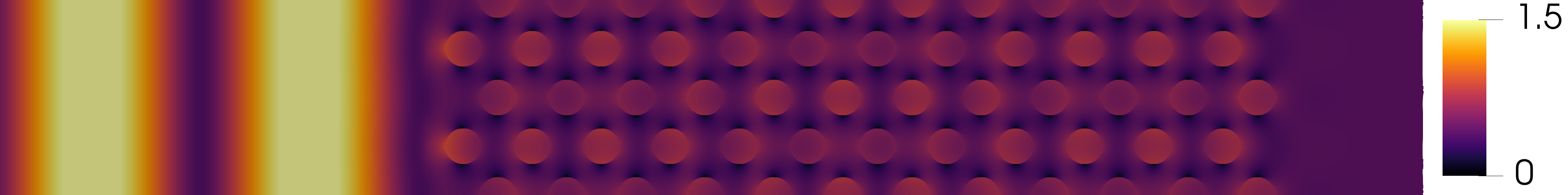 ;
{scope}[x=(image.south east),y=(image.north west)]
\draw[dashed,white] (1201/4400, 0) – (1201/4400,0.5);
;
{scope}[x=(image.south east),y=(image.north west)]
\draw[dashed,white] (1201/4400, 0) – (1201/4400,0.5);
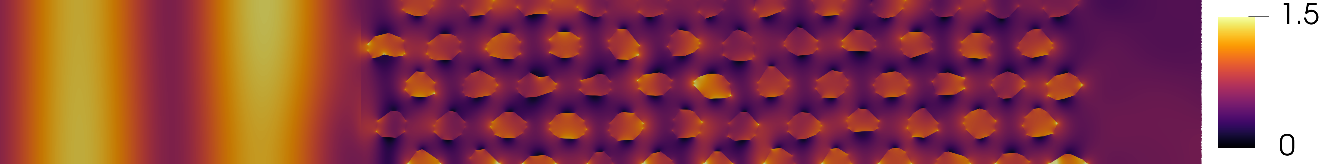
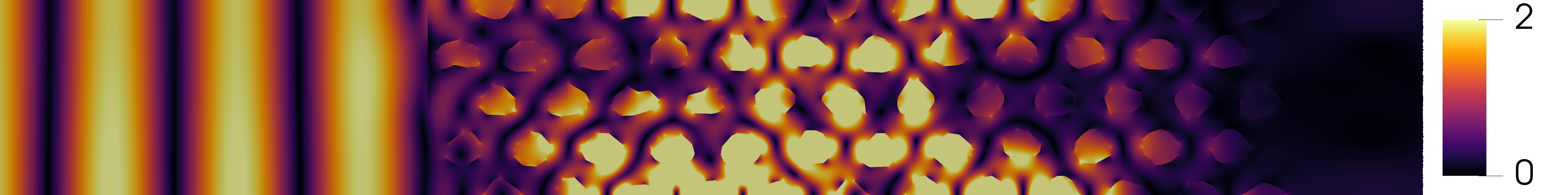
Figure 6 shows the field at , below the stopband in the fringe range (1a), where both crystals show clear Fabry-Pérot fringes without sharp peaks. The reconstructed and comparable design crystals have a transmission of 87% and 61% respectively, which is apparent in the different amplitude of the fringes in the air region. The field shows the outline of the pores, with the field inside the pores, and especially on the edges, being larger than in the silicon. If we compare patterns and field strengths around different pores in the same crystal we observe great similarity.
l0ptt0pt\tikzsetexternal/export next=true{tikzpicture}
\node[fill=white,inner sep=1,outer sep=1] at (0,0) (7);
{tikzpicture}
\node[anchor=south west,inner sep=0] (image) at (0,0)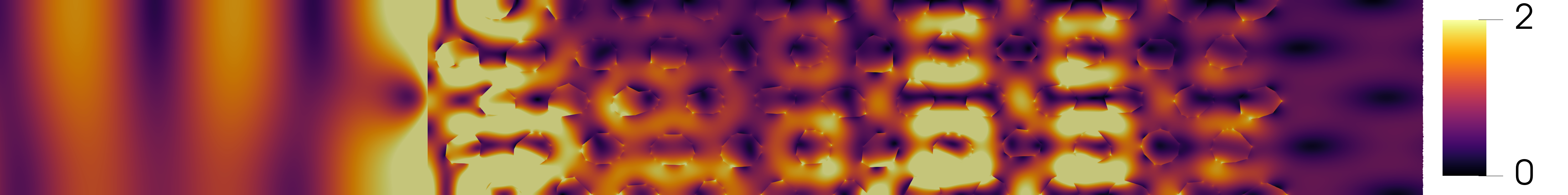 ;
{scope}[x=(image.south east),y=(image.north west)]
\draw[dashed] (270/4400, 0) – (200/4400,1);
\draw[dashed] (610/4400, 0) – (660/4400,1);
;
{scope}[x=(image.south east),y=(image.north west)]
\draw[dashed] (270/4400, 0) – (200/4400,1);
\draw[dashed] (610/4400, 0) – (660/4400,1);
l0ptt0pt\tikzsetexternal/export next=true{tikzpicture}
\node[fill=white,inner sep=1,outer sep=1] at (0,0) (7);
{tikzpicture}
\node[anchor=south west,inner sep=0] (image) at (0,0)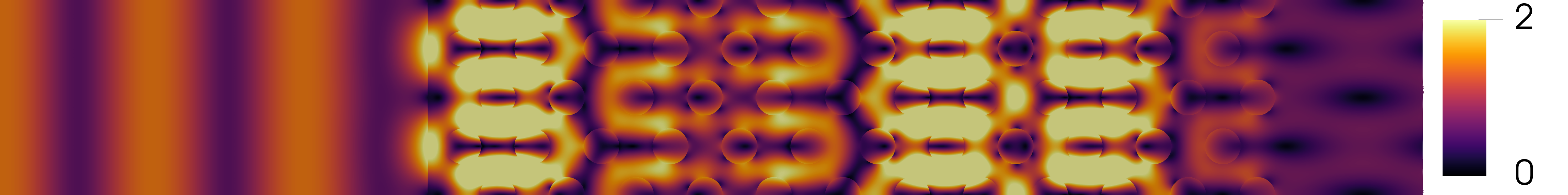 ;
{scope}[x=(image.south east),y=(image.north west)]
\draw[dashed,white] (1201/4400, 0) – (1201/4400,0.5);
;
{scope}[x=(image.south east),y=(image.north west)]
\draw[dashed,white] (1201/4400, 0) – (1201/4400,0.5);
Figure 7 shows the fields at , just below the stopband in the range of fringes and speckle (1c range). The transmission for the reconstructed and utopian crystal are almost the same at and . Nevertheless, there are significant differences between the field inside the real crystal and the utopian structure. In both crystals we observe that the field is strongest around the pores, but there is much more variation in the direction of propagation. For example, along the centerline of the crystal there are regions with almost zero field strength, and regions where the field is more than the incident field strength. Comparing the real crystal with the utopian one we observe that the real crystal shows additional differences in the transverse direction, with the field on the bottom side being on average stronger than on the top.
At the front surface of the crystal we observe two differences between the reconstructed and utopian crystals. Firstly, the interference pattern of the incident and reflected wave has a different angle with respect to the interface. For the reconstructed crystal this is slightly tilted as highlighted by the dashed lines, while for the utopian crystal it is perfectly vertical. The diagonal interference pattern for the real crystal is the result of reflecting part of the light into the first mode. The utopian crystal and the incident beam are symmetric along the center line of the domain, reflecting the incident light into the first mode is incompatible with this symmetry. The varied pores in the real crystal break this symmetry, and thus allow reflecting into the first mode. Secondly, we note that there is a large difference in the field strength on the air side of the crystal. In specific cases such difference could be very important, for example when placing quantum dots on the surface, but we do not have a good explanation for why it happens.
l0ptt0pt\tikzsetexternal/export next=true{tikzpicture}
\node[fill=white,inner sep=1,outer sep=1] at (0,0) (8);
l0ptt0pt\tikzsetexternal/export next=true{tikzpicture}
\node[fill=white,inner sep=1,outer sep=1] at (0,0) (8);
{tikzpicture}
\node[anchor=south west,inner sep=0] (image) at (0,0)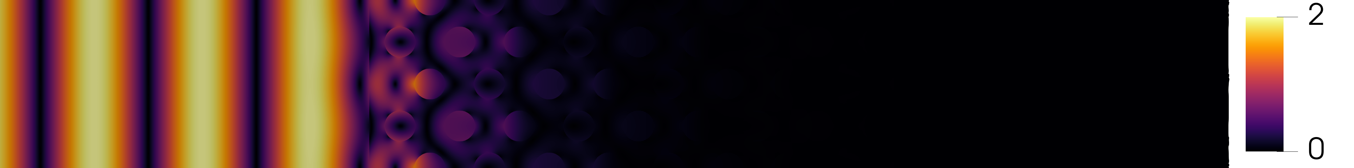 ;
{scope}[x=(image.south east),y=(image.north west)]
\draw[dashed,white] (1201/4400, 0) – (1201/4400,0.5);
;
{scope}[x=(image.south east),y=(image.north west)]
\draw[dashed,white] (1201/4400, 0) – (1201/4400,0.5);
Figure 8 shows the fields at . For the reconstructed crystal the transmission is , and the wavenumber is on the low-wavenumber side of a sharp transmission peak (that is not fully resolved by the computation, and whose maximum transmission is at least ). For the utopian crystal the wavenumber is inside the stopband and the transmission is thus vanishingly small.
While the reflection in both cases is almost complete, the field inside the crystal is radically different: In the reconstructed crystal the field has an amplitude comparable to the amplitude of the incident field, with regions where the field has more than the incident amplitude. The field is strongest in the bulk of the crystal away from the surfaces and reveals a random longitudinal and transverse distribution, somewhat similar to speckle in a (non-absorbing) random structure see, e.g., Ref. [68]. For the utopian crystal we observe that the field decays exponentially away from the front interface of the crystal to values below the computational accuracy. The Bragg length corresponding to this decay is , or about lattice constants in the propagating direction. This is much less than the size of the crystal in propagation direction (). Hence, since , the crystal is in the thick-crystal limit and the effects that we observe are bulk crystal effects with few surface effects expected.
Let us put this Bragg length in perspective with previous work: In Ref. [69] the Bragg length is derived from measurements of a real crystal with the same structure as studied here, but with slightly larger pores (, here ). Based on the relative width of the stopband they compute a Bragg length of , a bit larger than here. However, if we use the same derivation from the bandwidth in our spectra we get a Bragg length of , a close agreement. The difference between the Bragg length derived from spatial intensity decay (its definition) versus the one derived from stopband width is attributed to the fact that in the latter a weak photonic interaction assumption is made [60], that is clearly violated in silicon-air nanostructures. In Ref. [55] the Bragg length was computed for a 3D inverse woodpile by varying crystal thickness. Such a crystal is not directly comparable due to the difference in dimension (3D vs 2D). Nevertheless, by converting their Bragg value to our crystal size, we get for s and p-polarization, respectively, in reasonable mutual agreement.
5 Discussion
5.1 Utopian crystal as a model
In the vast majority of literature utopian models are used to predict or understand the optical properties of real crystals. By comparing the results of the real and utopian crystal we now address the question: “How accurate is the utopian model as predictor or source of explanations?”
We find that the frequency spectrum of the utopian model to be very ordered. Below the stopband there are Fabry-Pérot fringes, a short range of near-stopband effects, then a stopband, followed by ordered peaks above the stopband. Only part of this ordered structure is observed with the real crystal. Fabry-Pérot fringes are also present in the real crystal with accurately predicted spacing, but more varied amplitude. These fringes are only partially visible near the stopband, which we attributed to frequency speckle. The stopband and its lower band edge are accurately predicted, although the width is significantly smaller. The ordered peaks above the stopband of the utopian crystal completely miss the prediction of frequency speckle as with the real crystal.
In general we see that there is a better correspondence at low frequency than at high frequency. This is logical if we view the real crystal as a utopian crystal with additional scatterers from the deviating pores [22]. The frequency spectrum of the real crystal is then a combination of the ordered spectrum of the utopian crystal with additional features due to the inclusion of scatterers. The strength of these scatterers increases with frequency as their size relative to the wavelength increases. Correspondingly, the scattering mean free path due to all pore-variation scatterers decreases with frequency, increasing the effect of the scattering with respect to the background, and thereby decreasing the accuracy of the predictions from the utopian crystal.
With this model in mind we can also explain the great similarity of the electric fields at the lowest frequency. At such low frequency the pore-variation scatterers are very weakly scattering and the mean free path is much longer than the lattice size . This is backed up by the presence of Fabry-Pérot fringes in the spectrum as for a stronger scattering sample with the scattering would disrupt an interference effect like Fabry-Pérot fringes.
Two of these robust features, the frequency of the bandgap and the spacing of the Fabry-Pérot peaks can be predicted using the crystal lattice and volume fraction, but without considering the exact pore shapes. Specifically, consider the effective refractive index computed from the average dielectric constant [70] , where the averaging is done based on the silicon and air in a unit cell of the utopian crystal. Based on this and the length of the crystal , the Fabry-Pérot fringes are spaced at , while we observe to in excellent agreement. Similarly, by considering the crystal lattice and the corresponding Bragg peaks as in Ref. [23], we obtain an expected position of the stopband at , practically in the middle of the stopband of the real crystal and on the lower half of the utopian crystal.
While the utopian model adds the additional accurate prediction on the lower bound of the stopband, it is fundamentally unable to predict the speckle observed both above and below the stopband. This speckle is the result of the varied shapes and size of the pores, ultimately resulting from entropic effects in the manufacturing. These features are lacking in the utopian model, and that is precisely what makes the utopian model utopian.
5.2 Effects of boundary conditions
The two mirror boundary conditions in the computational setup were used because of the limited width of the dataset. The use of mirror boundary conditions gives realistic pores on the edges of the domain, but has as side effect that the computational domain forms a waveguide. The use of such a waveguide geometry rather than a freestanding crystal has two implications.
The first implication is that at a fixed frequency only a few propagating modes are available. This is especially important in the air region, where the cutoff frequency of the TE1 mode at is inside the relevant frequency range. Below this cutoff there is only a single propagating mode in the air region. Above this cutoff there are two propagating modes and we see two changes: there are no longer clear fringes in the transmission spectrum, and there is a reflection into the propagating mode. Clear fringes, like those below the cutoff frequency, are expected when the wavelength is too long to be affected by the very local variation in pore shapes. The sudden transition in our results at the cutoff of the mode is thus in all likelihood an artifact of our geometry. We expect that with a wider waveguide, and thus a lower cutoff frequency, the transition will happen at a lower frequency.
We note that the cutoff frequency for the air-mode is the same for the utopian design. However, the utopian crystal has a width of two unit cells. The symmetry in the domain implies that the utopian crystal can only reflect and transmit into the , , , etc. air and silicon modes [71]. In the computed spectral range, the utopian crystal has one mode for reflection and up to two for transmission, while the reconstructed crystal has up to three modes for reflection and up to seven for transmission.
The second implication is that each mode on the reflection and transmission side corresponds to a specific frequency-dependent angle. The current computational setup thus allows to describe only an incident wave at these specific angles. The extension to true angle resolved problems is theoretically simple. Applying the mirror boundary condition one gets periodic boundary conditions. Generalizing these to quasi-periodic would then support incident waves at arbitrary angles.
5.3 Reconstruction
An essential part of our study is the reconstruction process that was used to obtain the crystal structure from the X-ray data. Design choices such as representing the pore outline by a polygon, the algorithm used for the segmentation and the employed parameters all affect the shape and size of the pores in the reconstructed crystal, thereby affecting the transmission spectrum and electric fields presented here. However, the question is if the changes from a different design, algorithm or parameter will meaningfully influence the results and conclusions presented here. We discuss three different aspects of this question.
The effects of which segmentation algorithm is used and the subsequent choice for its parameters are naturally intertwined. Ideally, the effects are quantified through sensitivity analysis, but that is a laborious task, hence we take an alternative approach. Both the algorithm and parameter choices influence the size of the pores and their shapes and thus the resulting transmission spectra.
Firstly, we study the effect of the pore shapes. The reconstructed crystal consist of pores each with a different shape. Thus, it is extremely unlikely that any similarities between the spectrum of the reconstructed and utopian crystals are accidental. It is far more likely, as we concluded, that these similarities are robust with respect to deviations in the pore shape.
Secondly, we consider the effect of varying the pore size. The effect of the pore size is taken into account by matching the pore size of the utopian crystal to that of the reconstructed crystal. Hence, the pore size cannot be the source of the differences between the reconstructed and utopian crystals. The strong influence on the similarities between the spectra of the reconstructed and utopian crystals is seen from the comparison with the effective refractive index model. The only free parameter in this model is the effective refractive index, which follows from the pore size via the silicon air ratio. The fact that this model accurately predicts the similarities shows both that the pore size is important for the actual spectrum, and that it can predict its effects.
Thirdly, the reconstruction algorithm reconstructs the air-silicon interface as a polygon. Such a polygon has corners, and these are known to create locally very strong fields from corner singularities [72]. Indeed, in the computed electric fields we observe locally very strong fields at the corners of the pores. The X-ray data does not have sufficient resolution to determine whether such corners exist, and we do not necessarily expect them from the manufacturing process. Therefore, it is not unlikely that the air-silicon boundary is smoother in the original crystal than in the reconstructed crystal. Such a smoother boundary could be made by describing the interface by curved line segments. The usefulness of doing this depends on what the results are used for. Curved boundaries will remove or reduce the corner singularities and locally reduce the very extreme fields. We expect that the effect on global properties like the transmission is limited, but that it is more important for local quantities like the LDOS.
5.4 Outlook: real crystal computation
The computation presented here is a first demonstration of a data-driven photonic crystal computation. We envision three broad directions how our method can be extended.
Firstly, the computations presented here consider a plane wave incident on a 2D waveguide setup, which is unlike the experimental setup of focussing a beam on a 3D finite size crystal. A better understanding of the experimental situation will be gained by changing the computational setup to more closely align with reality. A computation of a completely realistic situation is far beyond current computational capabilities, but understanding the effects of individual differences such as the finite width or 2D structure are more realistic.
A second direction is to consider several forms of sensitivity analysis based on the current computational setup. The sensitivity of the results with respect to the parameters used in the reconstruction will give a more rigorous idea on how accurate we need to be in the reconstruction. This could be used to verify our expectation that the spectral features that are shared by the reconstructed and utopian crystals are relatively robust. Moreover, looking at sensitivity to local deformations of the pore shapes may provide better insight into whether there are types of deviations that more strongly influence the performance of the crystal structure and thus require attention in the manufacturing process.
A third direction is to focus on how accurate the reconstruction of the real crystal is, with the goal of creating the perfect reconstruction for the best comparison with experimental work. The current approach to the reconstruction and especially the selection of the parameters is based on visual judgment of the result. One consequence of this is that the pore size is likely different from that of the actual crystal. Such differences could be resolved by calibrating the reconstruction process against the actual structure. Such a calibrated reconstruction will provide a better candidate for a comparison between computation and actual measurements, and therefore understanding of the individual sample.
6 Conclusions
In conclusion, we have developed and presented a new data-driven approach to computational nanophotonics. The essence of this approach is to use a reconstruction of a real nanostructure, including all its manufacturing deviations. These deviations significantly impact the optical performance of real nanostructures, but are absent from traditional computational nanophotonics where one considers structures so perfect that they can only be made in a manufacturing Utopia. Comparison of traditional computational results with real measurements is thus fraught with many possible causes of differences, but there is no way to distinguish between them. Our method provides an intermediate between these two extremes that allows better understanding in the relevance of theoretical results and insight in the working of actual devices.
To demonstrate our new method, we apply it to a X-ray imaging reconstruction of a photonic bandgap crystal with inverse woodpile structure. This is done by processing a 2D slice from the reconstruction in a computational mesh. This mesh is then used to compute the transmission through the reconstructed crystal over a broad frequency range. For a comparison with existing models we consider the transmission through a matching utopian crystal, a crystal with perfectly round pores and matching fill fraction.
For the reconstructed crystal we observe Fabry-Pérot fringes, a stopband and frequency speckle. The utopian model shows similar Fabry-Pérot fringes and a slightly wider stopband. The speckle seen with the reconstructed crystal is completely absent from the utopian model, and the transmission above the stopband is thus completely different.
The use of computational methods allows, unlike experiments, to study the fields everywhere inside the crystal in detail. We have thus compared the fields inside the reconstructed and utopian crystal at three sample frequencies. We observed major differences in the fields at constant frequency, which are not apparent from external probes like transmission.
Funding NWO JCSER Program, project 680-91-084, Accurate and Efficient Computation of the optical properties of nanostructures for improved photovoltaics. NWO (FOM) program nr. 138 “Stirring of light!”. NWO-TTW program P15-36 “Free-Form Scattering Optics” (FFSO).
Acknowledgments We thank Peter Cloetens, Melissa Goodwin, Diana Grishina, Cock Harteveld, Jens Wehner for help. We thank ESRF for beamtime through experiments HC-2520 and CH-5092.
Disclosures The authors declare no conflicts of interest.
Data availability Data underlying the results presented in this paper are available in Ref. [46]. The original 3D dataset is not publicly available at this time but may be obtained from the authors upon reasonable request.
Supplemental document See Supplement 1 for supporting content.
References
- [1] J. D. Joannopoulos, S. G. Johnson, J. N. Winn, and R. D. Meade, Photonic crystals: molding the flow of light (Princeton University Press, Princeton, 2008), 2nd ed.
- [2] J.-M. Lourtioz, H. Benisty, V. Berger, et al., Photonic Crystals (Springer-Verlag, Berlin, 2008), 2nd ed.
- [3] L. Novotny and B. Hecht, Principles of Nano-Optics (Cambridge University Press, 2012), 2nd ed.
- [4] N. W. Ashcroft and N. D. Mermin, Solid State physics (Brooks/Cole, Belmont, 1976).
- [5] E. Economou, The Physics of Solids (Springer-Verlag, 2010).
- [6] A. A. Asatryan, K. Busch, R. C. McPhedran, et al., “Two-dimensional Green’s function and local density of states in photonic crystals consisting of a finite number of cylinders of infinite length,” \JournalTitlePhysical Review E 63, 046612 (2001).
- [7] S. B. Hasan, A. P. Mosk, W. L. Vos, and A. Lagendijk, “Finite-size Scaling of the Density of States in Photonic Band Gap Crystals,” \JournalTitlePhysical Review Letters 120, 237402 (2018).
- [8] S. E. Skipetrov, “Finite-size scaling of the density of states inside band gaps of ideal and disordered photonic crystals,” \JournalTitleThe European Physical Journal B 93, 70 (2020).
- [9] V. P. Bykov, “Spontaneous emission from a medium with a band spectrum,” \JournalTitleSoviet Journal of Quantum Electronics 4, 861 (1975).
- [10] E. Yablonovitch, “Inhibited Spontaneous Emission in Solid-State Physics and Electronics,” \JournalTitlePhysical Review Letters 58, 2059–2062 (1987).
- [11] P. Bermel, C. Luo, L. Zeng, et al., “Improving thin-film crystalline silicon solar cell efficiencies with photonic crystals,” \JournalTitleOptics Express 15, 16986–17000 (2007).
- [12] R. B. Wehrspohn and J. Üpping, “3D photonic crystals for photon management in solar cells,” \JournalTitleJournal of Optics 14, 024003 (2012).
- [13] A. Tandaechanurat, S. Ishida, D. Guimard, et al., “Lasing oscillation in a three-dimensional photonic crystal nanocavity with a complete bandgap,” \JournalTitleNature Photonics 5, 91–94 (2011).
- [14] C. M. Cornelius and J. P. Dowling, “Modification of Planck blackbody radiation by photonic band-gap structures,” \JournalTitlePhysical Review A 59, 4736–4746 (1999).
- [15] J. G. Fleming, S. Y. Lin, I. El-Kady, et al., “All-metallic three-dimensional photonic crystals with a large infrared bandgap,” \JournalTitleNature 417, 52–55 (2002).
- [16] J. Wang and M. Qi, “Design of a compact mode and polarization converter in three-dimensional photonic crystals,” \JournalTitleOptics Express 20, 20356–20367 (2012).
- [17] T. Ergin, N. Stenger, P. Brenner, et al., “Three-Dimensional Invisibility Cloak at Optical Wavelengths,” \JournalTitleScience 328, 337–339 (2010).
- [18] K. Ishizaki, M. Koumura, K. Suzuki, et al., “Realization of three-dimensional guiding of photons in photonic crystals,” \JournalTitleNature Photonics 7, 133–137 (2013).
- [19] T. Tajiri, S. Takahashi, Y. Ota, et al., “Three-dimensional photonic crystal simultaneously integrating a nanocavity laser and waveguides,” \JournalTitleOptica 6, 296–299 (2019).
- [20] S. Fan, P. R. Villeneuve, and J. D. Joannopoulos, “Theoretical investigation of fabrication-related disorder on the properties of photonic crystals,” \JournalTitleJournal of Applied Physics 78, 1415–1418 (1995).
- [21] A. F. Koenderink and W. L. Vos, “Light exiting from real photonic band gap crystals is diffuse and strongly directional,” \JournalTitlePhys. Rev. Lett. 91, 213902 (2003).
- [22] A. F. Koenderink, A. Lagendijk, and W. L. Vos, “Optical extinction due to intrinsic structural variations of photonic crystals,” \JournalTitlePhysical Review B 72, 153102 (2005).
- [23] S. R. Huisman, R. V. Nair, A. Hartsuiker, et al., “Observation of Sub-Bragg Diffraction of Waves in Crystals,” \JournalTitlePhysical Review Letters 108, 083901 (2012).
- [24] M. Adhikary, R. Uppu, C. A. M. Harteveld, et al., “Experimental probe of a complete 3D photonic band gap,” \JournalTitleOpt. Express, OE 28, 2683–2698 (2020).
- [25] K. Busch, M. König, and J. Niegemann, “Discontinuous Galerkin methods in nanophotonics,” \JournalTitleLaser & Photonics Reviews 5, 773–809 (2011).
- [26] S. G. Johnson and J. D. Joannopoulos, “Block-iterative frequency-domain methods for Maxwell’s equations in a planewave basis,” \JournalTitleOptics Express 8, 173–190 (2001).
- [27] K. Yee, “Numerical solution of initial boundary value problems involving maxwell’s equations in isotropic media,” \JournalTitleIEEE Transactions on Antennas and Propagation 14, 302–307 (1966).
- [28] Y. A. Vlasov, M. Deutsch, and D. J. Norris, “Single-domain spectroscopy of self-assembled photonic crystals,” \JournalTitleApplied Physics Letters 76, 1627–1629 (2000).
- [29] D. A. Grishina, C. A. M. Harteveld, A. Pacureanu, et al., “X-ray Imaging of Functional Three-Dimensional Nanostructures on Massive Substrates,” \JournalTitleACS Nano 13, 13932–13939 (2019).
- [30] E. Flück, N. F. van Hulst, W. L. Vos, and L. Kuipers, “Near-field optical investigation of three-dimensional photonic crystals,” \JournalTitlePhysical Review E 68, 015601 (2003).
- [31] S. Hughes, L. Ramunno, J. F. Young, and J. E. Sipe, “Extrinsic Optical Scattering Loss in Photonic Crystal Waveguides: Role of Fabrication Disorder and Photon Group Velocity,” \JournalTitlePhysical Review Letters 94, 033903 (2005).
- [32] Ultimately the fabrication imperfections are limited by the entropy at the finite temperature in a cleanroom. In practice, imperfections are much larger and caused by a plethora of imperfections in fabrication equipment and processes.
- [33] L. A. Woldering, A. P. Mosk, R. W. Tjerkstra, and W. L. Vos, “The influence of fabrication deviations on the photonic band gap of three-dimensional inverse woodpile nanostructures,” \JournalTitleJournal of Applied Physics 105, 093108 (2009).
- [34] J. E. G. J. Wijnhoven, L. Bechger, and W. L. Vos, “Fabrication and Characterization of Large Macroporous Photonic Crystals in Titania,” \JournalTitleChem. Mater. 13, 4486–4499 (2001).
- [35] W. R. Frei and H. T. Johnson, “Finite-element analysis of disorder effects in photonic crystals,” \JournalTitlePhysical Review B 70, 165116 (2004).
- [36] L. E. Reichl, A Modern Course in Statistical Physics (Wiley-VCH, Weinheim, 2016), 4th ed.
- [37] K. M. Ho, C. T. Chan, C. M. Soukoulis, et al., “Photonic band gaps in three dimensions: New layer-by-layer periodic structures,” \JournalTitleSolid State Communications 89, 413–416 (1994).
- [38] M. Maldovan and E. L. Thomas, “Diamond-structured photonic crystals,” \JournalTitleNature Mater 3, 593–600 (2004).
- [39] D. A. Grishina, C. A. M. Harteveld, L. A. Woldering, and W. L. Vos, “Method for making a single-step etch mask for 3D monolithic nanostructures,” \JournalTitleNanotechnology 26, 505302 (2015).
- [40] A. S. Schulz, C. A. M. Harteveld, G. J. Vancso, et al., “Targeted Positioning of Quantum Dots Inside 3D Silicon Photonic Crystals Revealed by Synchrotron X-ray Fluorescence Tomography,” \JournalTitleACS Nano 16, 3674–3683 (2022).
- [41] M. J. Goodwin, C. A. M. Harteveld, M. J. d. Boer, and W. L. Vos, “Deep reactive ion etching of cylindrical nanopores in silicon for photonic crystals,” \JournalTitleNanotechnology 34, 225301 (2023).
- [42] P. Cloetens, W. Ludwig, J. Baruchel, et al., “Holotomography: Quantitative phase tomography with micrometer resolution using hard synchrotron radiation x rays,” \JournalTitleApplied Physics Letters 75, 2912–2914 (1999).
- [43] A. Fraczkiewicz, F. Lorut, G. Audoit, et al., “3D high resolution imaging for microelectronics: A multi-technique survey on copper pillars,” \JournalTitleUltramicroscopy 193, 71–83 (2018).
- [44] K. P. Furlan, E. Larsson, A. Diaz, et al., “Photonic materials for high-temperature applications: Synthesis and characterization by X-ray ptychographic tomography,” \JournalTitleApplied Materials Today 13, 359–369 (2018).
- [45] S. Smeets, N. Renaud, and L. J. Corbijn van Willenswaard, “Nanomesh: A Python workflow tool for generating meshes from image data,” \JournalTitleJournal of Open Source Software 7, 4654 (2022).
- [46] L. Corbijn van Willenswaard, “Data: Non-utopian optical properties computed of a tomographically reconstructed real photonic band gap crystal [data set],” Zenodo (2023). https://doi.org/10.5281/zenodo.10419091.
- [47] R. Gonzalez and R. Wood, Digital Image Processing (Prentice Hall, 2002), 2nd ed.
- [48] S. van der Walt, J. L. Schönberger, J. Nunez-Iglesias, et al., “scikit-image: image processing in Python,” \JournalTitlePeerJ 2 (2014).
- [49] W. E. Lorensen and H. E. Cline, “Marching cubes: A high resolution 3D surface construction algorithm,” \JournalTitleACM SIGGRAPH Computer Graphics 21, 163–169 (1987).
- [50] L. A. Woldering, R. W. Tjerkstra, H. V. Jansen, et al., “Periodic arrays of deep nanopores made in silicon with reactive ion etching and deep UV lithography,” \JournalTitleNanotechnology 19, 145304 (2008).
- [51] I. Perugia, D. Schötzau, and P. Monk, “Stabilized interior penalty methods for the time-harmonic Maxwell equations,” \JournalTitleComputer Methods in Applied Mechanics and Engineering 191, 4675–4697 (2002).
- [52] P. Houston, I. Perugia, A. Schneebeli, and D. Schötzau, “Interior penalty method for the indefinite time-harmonic Maxwell equations,” \JournalTitleNumerische Mathematik 100, 485–518 (2005).
- [53] D. Sármány, F. Izsák, and J. J. W. van der Vegt, “Optimal Penalty Parameters for Symmetric Discontinuous Galerkin Discretisations of the Time-Harmonic Maxwell Equations,” \JournalTitleJournal of Scientific Computing 44, 219–254 (2010).
- [54] K. Liu, D. Gallistl, M. Schlottbom, and J. J. W. van der Vegt, “Analysis of a mixed discontinuous Galerkin method for the time-harmonic Maxwell equations with minimal smoothness requirements,” \JournalTitleIMA Journal of Numerical Analysis 43, 2320–2351 (2023).
- [55] D. Devashish, S. B. Hasan, J. J. W. van der Vegt, and W. L. Vos, “Reflectivity calculated for a three-dimensional silicon photonic band gap crystal with finite support,” \JournalTitlePhysical Review B 95, 155141 (2017).
- [56] J. D. Jackson, Classical electrodynamics; 2nd ed. (Wiley, New York, NY, 1975).
- [57] J.-P. Berenger, “A perfectly matched layer for the absorption of electromagnetic waves,” \JournalTitleJournal of Computational Physics 114, 185–200 (1994).
- [58] P. Monk, Finite Element Methods for Maxwell’s Equations (Oxford University Press, 2003).
- [59] S. Datta, C. T. Chan, K. M. Ho, and C. M. Soukoulis, “Effective dielectric constant of periodic composite structures,” \JournalTitlePhysical Review B 48, 14936–14943 (1993).
- [60] W. L. Vos, R. Sprik, A. van Blaaderen, et al., “Strong effects of photonic band structures on the diffraction of colloidal crystals,” \JournalTitlePhysical Review B 53, 16231–16235 (1996).
- [61] E. Hecht and A. Zajac, Optics (Addison-Wesley Publishing Company, Reading MA, 1974).
- [62] P. Yeh, A. Yariv, and C.-S. Hong, “Electromagnetic propagation in periodic stratified media. I. General theory,” \JournalTitleJournal of the Optical Society of America 67, 423–438 (1977).
- [63] M. C. W. van Rossum and T. M. Nieuwenhuizen, “Multiple scattering of classical waves: microscopy, mesoscopy, and diffusion,” \JournalTitleRev. Mod. Phys. 71, 313–371 (1999).
- [64] V. Savona, “Electromagnetic modes of a disordered photonic crystal,” \JournalTitlePhysical Review B 83, 085301 (2011).
- [65] S. R. Huisman, G. Ctistis, S. Stobbe, et al., “Measurement of a band-edge tail in the density of states of a photonic-crystal waveguide,” \JournalTitlePhysical Review B 86, 155154 (2012).
- [66] P. Sheng, Introduction to Wave Scattering, Localization and Mesoscopic Phenomena (Springer-Verlag, Heidelberg, 2006), 2nd ed.
- [67] M. Kozoň, A. Lagendijk, M. Schlottbom, et al., “Scaling Theory of Wave Confinement in Classical and Quantum Periodic Systems,” \JournalTitlePhysical Review Letters 129, 176401 (2022).
- [68] S. F. Liew, S. M. Popoff, A. P. Mosk, et al., “Transmission channels for light in absorbing random media: From diffusive to ballistic-like transport,” \JournalTitlePhys. Rev. B 89, 224202 (2014).
- [69] R. Uppu, M. Adhikary, C. A. Harteveld, and W. L. Vos, “Spatially Shaping Waves to Penetrate Deep inside a Forbidden Gap,” \JournalTitlePhys. Rev. Lett. 126, 177402 (2021).
- [70] R. D. Meade, A. M. Rappe, K. D. Brommer, et al., “Accurate theoretical analysis of photonic band-gap materials,” \JournalTitlePhys. Rev. B 48, 8434–8437 (1993).
- [71] The waveguide domain can be seen as one mirror half of a periodic domain, where the guided modes correspond to solutions that are commensurate with the periodicity. This periodicity of the crystal corresponds to unit cells of the utopian crystal. Hence, the utopian crystal can only use every fourth waveguide mode.
- [72] M. Costabel and M. Dauge, “Singularities of Electromagnetic Fields in Polyhedral Domains,” \JournalTitleArchive for Rational Mechanics and Analysis 151, 221–276 (2000).