Effect of junction critical current disorder in superconducting quantum interference filter arrays
Abstract
In this study, we investigated the performance of two 2D superconducting quantum interference filter (SQIF) arrays fabricated from YBCO thin films at a temperature of 77 K. Each array consisted of 6 Josephson junctions (JJs) in parallel and 167 in series. We conducted both experimental and theoretical analyses, measuring the arrays’ voltage responses to an applied magnetic field and their voltage versus bias-current characteristics. To properly model the planar array layouts, our theoretical model used the stream function approach and also included the Johnson noise in the JJs. The model further divides the superconducting current density of the arrays into its Meissner current, circulating current, and bias current parts for practicality. Since the fabrication process of YBCO thin films cannot produce identical JJ critical currents, we assumed a log-normal distribution to model the JJ critical current disorder. Our model predictions, with a JJ critical current spread of 50%, agreed well with our experimental data. Using our model, we were able to study the dependence of the voltage modulation depth on critical current disorder and London penetration depth. We also analyzed the observed reflection asymmetries of the voltage versus magnetic field characteristics, which might provide insight into the degree of critical current disorder. Overall, our findings suggest that the use of YBCO thin films in SQIF arrays is promising, despite the critical current disorder inherent in their fabrication process. Our study highlights the importance of theoretical modeling in understanding the performance of superconducting devices and provides insights that could inform the design of future SQIF arrays.
I Introduction
When fabricating 2D superconducting quantum interference filter (SQIF) arrays (or superconducting quantum interference (SQUID) arrays) from YBCO thin films, the critical currents and electric resistances of the Josephson junctions (JJs) exhibit significant variability and thus have wide distributions. This --disorder in the arrays is thought to result in a decrease in the magnetic-field-to-voltage transfer function of the array, which is an undesirable outcome as the goal is typically to achieve a transfer function that is as large as possible for optimal performance in applications. How detrimental such an --disorder is in real devices, is still unknown. This is in contrast to low-temperature superconducting thin-film arrays, where the and values can be well controlled.
In this paper, we aim to provide a quantitative analysis of the impact of the --disorder on the performance of two specific YBCO 2D SQIF arrays that we have recently fabricated and measured. Our discussion will focus on the effects of --disorder in these particular arrays, while the broader impact of --disorder on 2D SQIF (or SQUID) arrays of varying dimensions and with different screening and thermal noise parameters will be addressed in a forthcoming publication.
Previously, we extensively modeled a structurally wide, thin-film 1D parallel SQUID array with center current biasing and used a brute-force approach to calculate the voltage-to-magnetic-field characteristics, as described in reference [1]. In the present paper, we use an improved version of our previous model, where we separate the superconducting current density into its Meissner current, circulating loop currents, and bias-current components. This separation allows us to save significant computational time and accurately calculate larger 2D arrays with strong --disorder.
Previous theoretical studies on 1D and 2D SQUID [2, 3, 4, 5], SQIF [6] and JJ [7] arrays have often not considered the effects of thermal noise. Recent research has shown that properly accounting for thermal noise is essential for accurately calculating the voltage-to-magnetic-field characteristics and transfer function of these arrays [8, 9, 10]. Only a few studies so far have investigated the consequences of --disorder in arrays [11, 5, 12], but direct comparisons with experimental data from genuine arrays with wide thin-film structures are lacking.
In this paper, we begin by discussing the layout, fabrication, and measurement setup of our 2D SQIF arrays in Section II. We then present our experimental results in Section III. In Section IV, we outline our theoretical model, including the JJ phase dynamics and the stream function approach. In Section V, we compare our experimental data with our model calculations and discuss the insights gained from our detailed theoretical calculations with emphasis on the --disorder. We summarize our findings in Section VI. Appendices are included to provide guidance on how to obtain the effective hole areas and the geometric and kinetic inductances.
II 2D SQIF array layout, fabrication and measurement setup
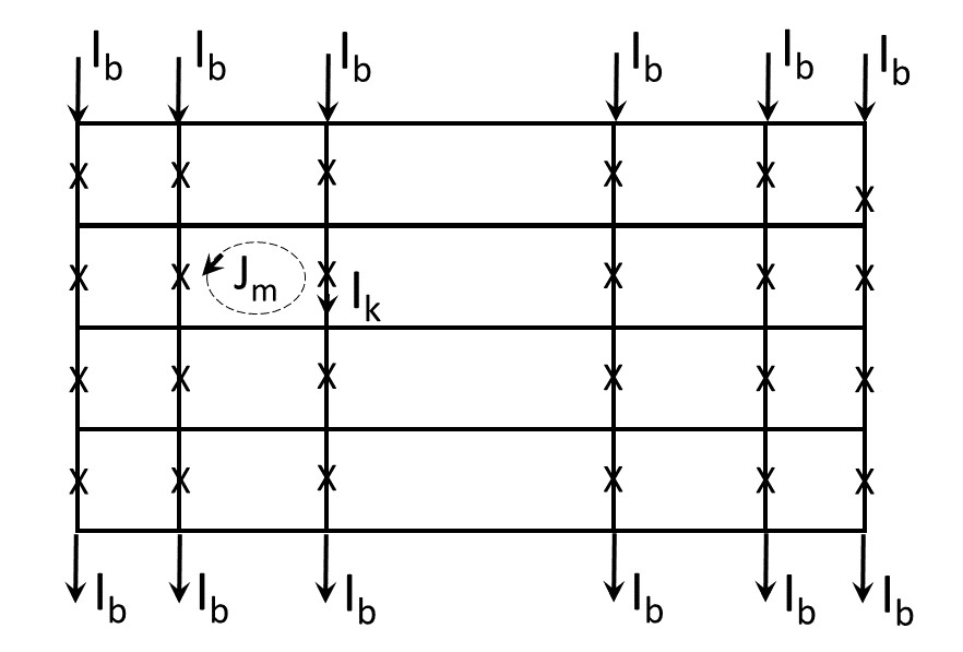
Two different SQIF arrays were fabricated lithographically from a thin-film of YBCO grown by e-beam evaporation on a 1 cm2 MgO substrate. The thickness of the film was =113 nm and its superconducting transition temperature was K. Before film deposition, steps were etched into the MgO surface (see Fig. 1) using a well established technique based on argon milling [13, 14]. During YBCO thin-film deposition, grain boundaries form along the edges of the sharp MgO steps, producing JJs. Films were then lithographically patterned into two different 2D SQIF arrays referred to in the following as arrays S1 and S2, which are displayed in Fig. 1.
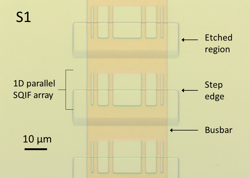
Each array consists of identical 1D parallel SQIF arrays (the rows) which are connected in series via superconducting YBCO thin-film busbars. Each 1D SQIF array has = 6 JJs in parallel. Table I lists the design parameters of S1 and S2, i.e. the SQIF hole height, the hole widths (left to right), the busbar height, and the number of identical 1D parallel SQIF arrays connected in series. The tracks leading to the JJ’s have the same width as the JJs themselves (Table I). Both arrays have geometric left-right symmetry. Because of the difficulty controlling grain boundary growth, the values of the critical currents and resistances ( = 1 to ) of the JJs can vary widely [15]. This disorder in and negatively affects the applied magnetic field to voltage transduction. In a 2D array, it is not possible to measure the and values individually and only consequences of the --disorder can be detected.
| # | hole height | hole widths L-R | busbar height | JJ width | |
|---|---|---|---|---|---|
| [ m ] | [ m ] | [ m ] | [m] | ||
| S1 | 15 | 1, 5, 13, 5, 1 | 16 | 2 | 167 |
| S2 | 15 | 8, 12, 20, 12, 8 | 16 | 2 | 167 |
For measurements, the arrays were placed on a measurement probe and dipped into a dewar of liquid nitrogen and zero field cooled from room temperature down to 77 K. To screen out the earth’s magnetic field, the dewar was surrounded by five layers of mu-metal shielding. The standard four-terminal method was used to measure the DC voltages appearing between the ends (between top and bottom) of the 2D SQIF arrays, while a bias current was injected at the top and exited the array at the bottom. A solenoid surrounding the probe enabled us to generate a homogeneous perpendicular applied magnetic field at the array. Both and of S1 and S2 were measured at 77 K.
III Experimental results
Figure 2 shows the experimental results of voltage versus the applied magnetic field for arrays S1 and S2, where was varied from to .
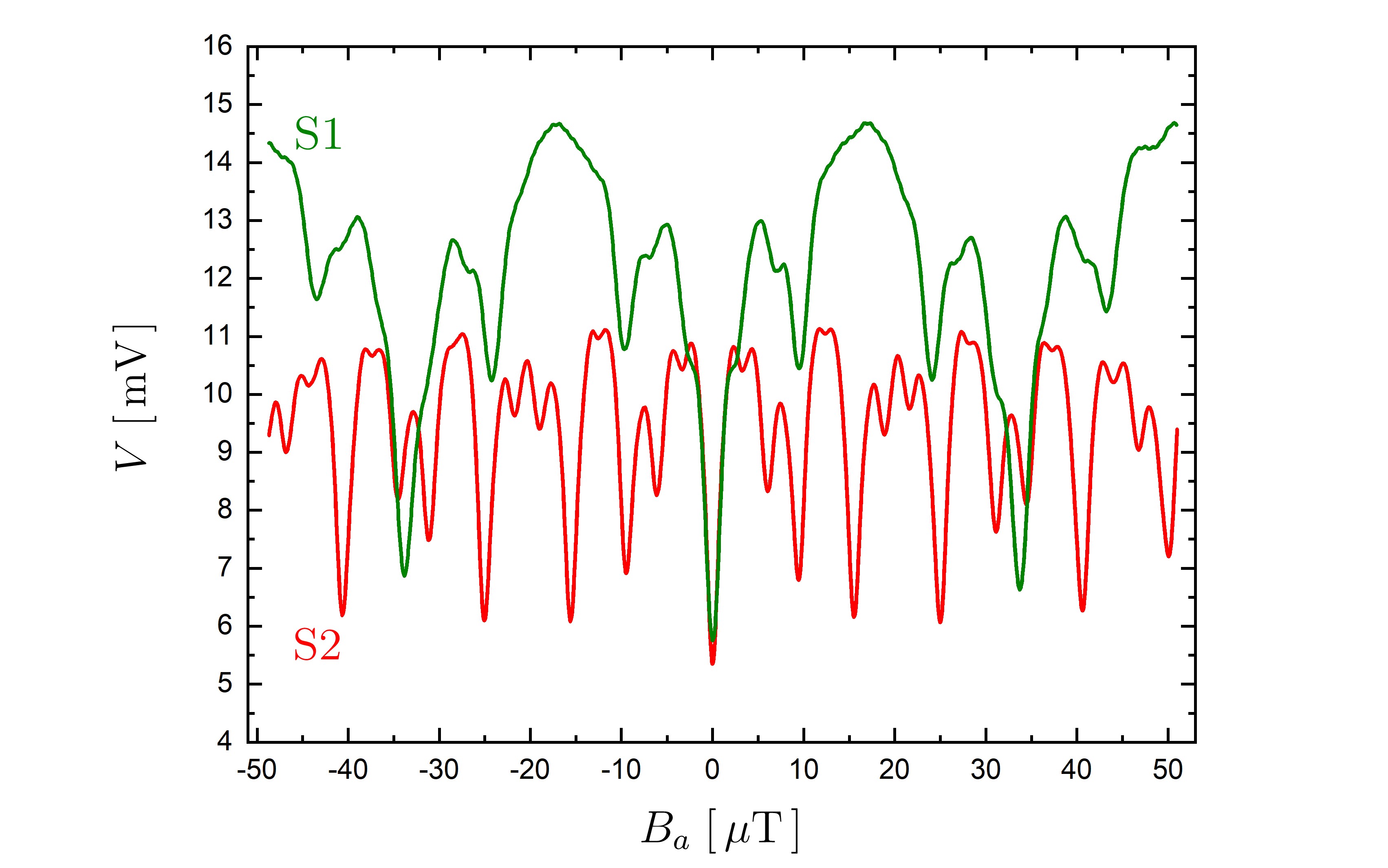
The bias currents for S1 and S2 were chosen to optimize the voltage modulation depths . can be used as a measure of the maximum transfer function of the center dip [8]. The values of the optimal bias current and are given in Table II. Both curves are nearly reflection symmetric with respect to the center dip. Because the rectangular holes in S2 are overall larger than those in S1, the characteristics of array S2 shows more oscillations in Fig. 2 than S1. To understand the origin of the complex shapes of these two characteristics, we have performed theoretical modeling which is outlined in detail below.
| # | [ A ] | [mV] | [ ] |
|---|---|---|---|
| S1 | 76.474 | 8.52 | 406.0 |
| S2 | 78.215 | 5.76 | 399.1 |
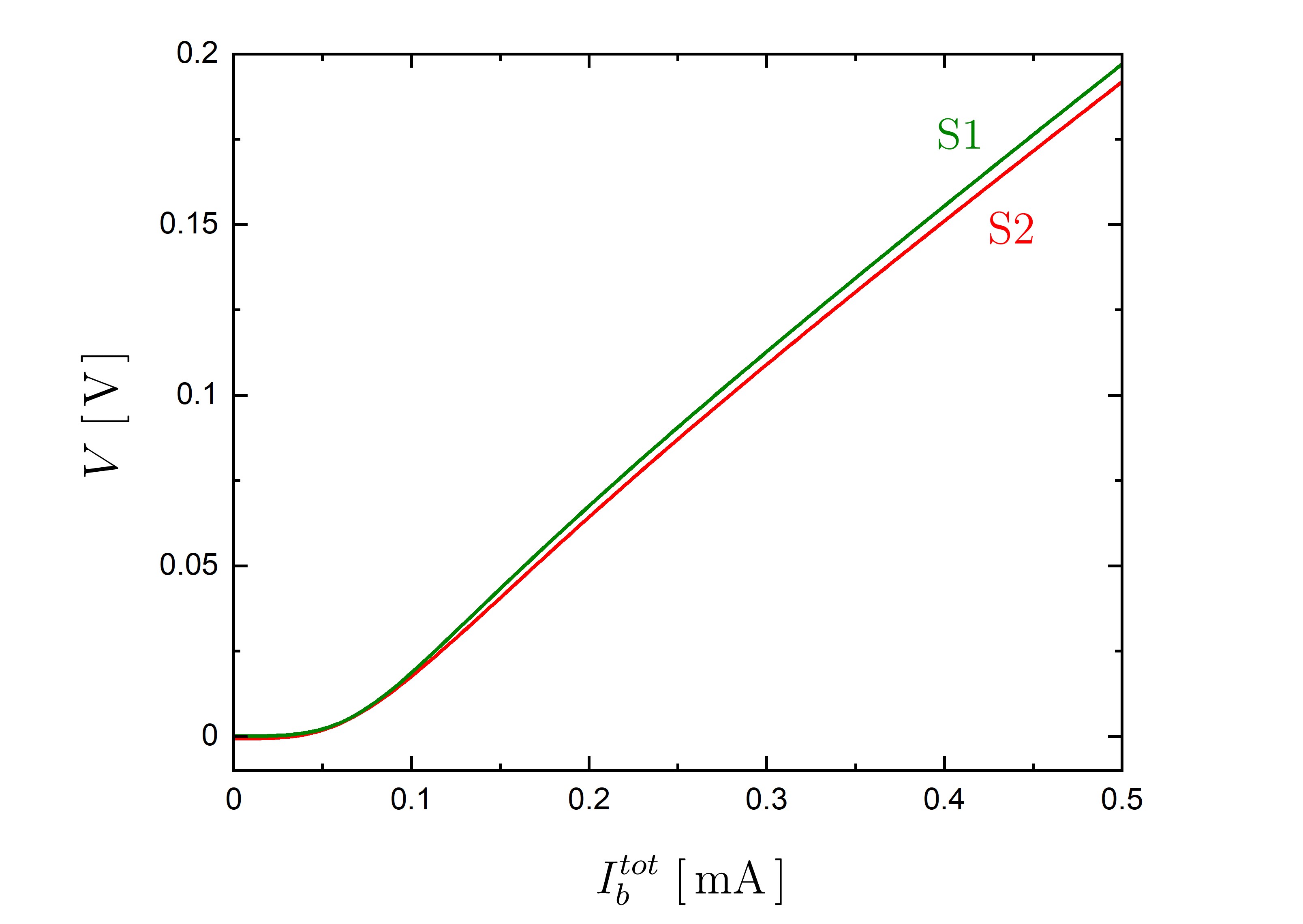
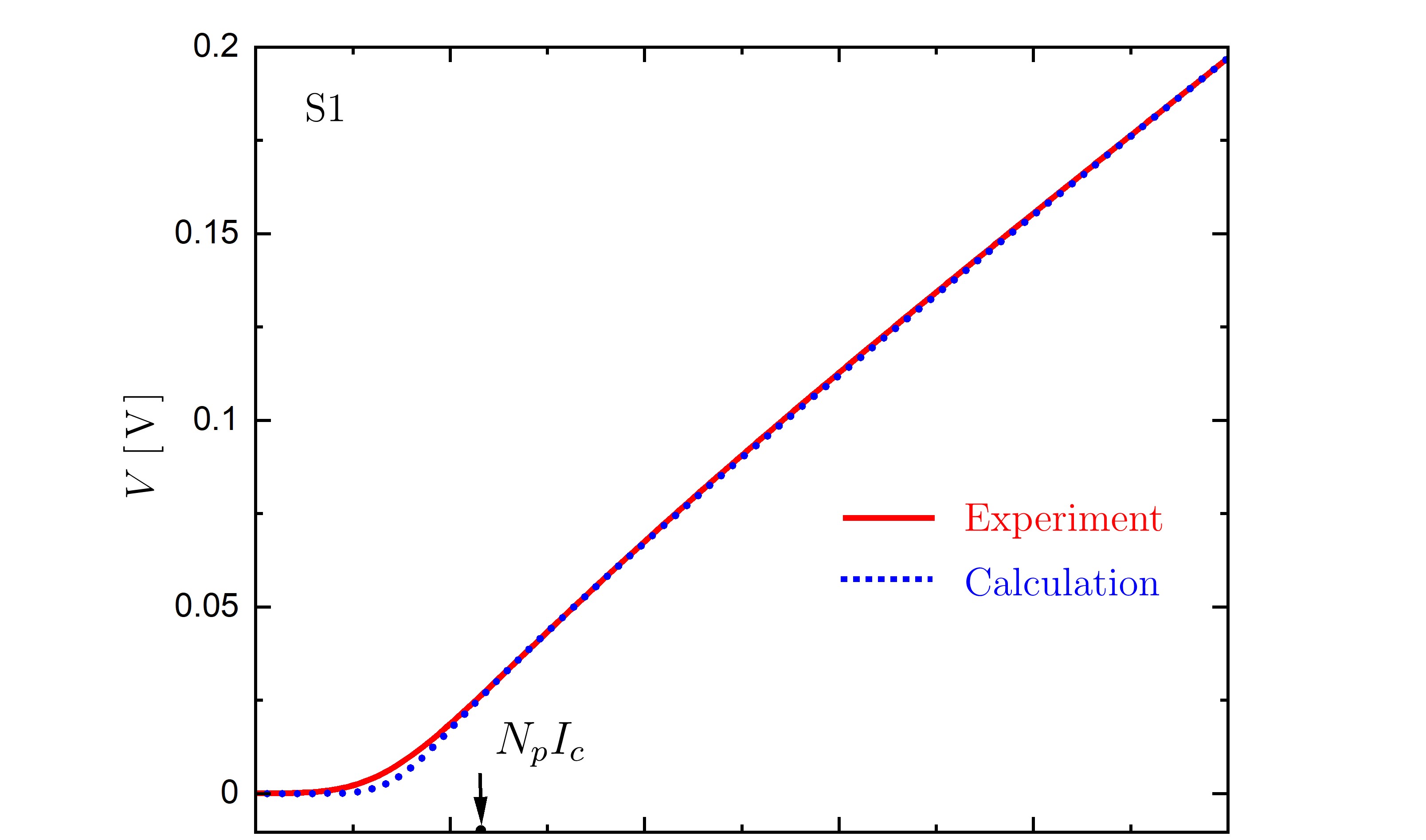
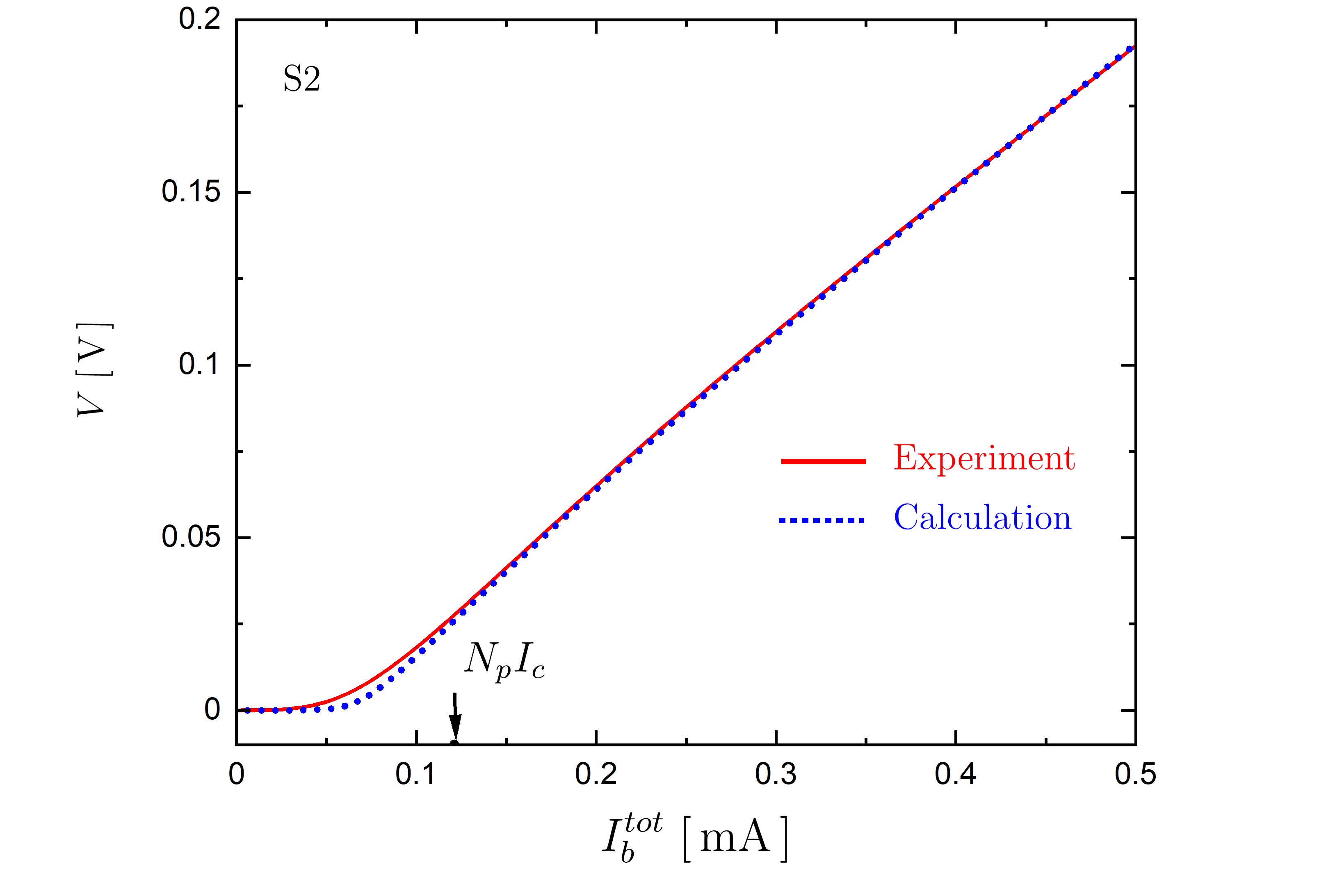
Figure 3 displays the results of our characteristics measurements in zero magnetic field for S1 and S2. The differential resistance at large defines the total resistance of the array which is given in Table II. Our theoretical modeling results in Section V will give an explanation for the shape of .
Section IV below will outline the theoretical model that we use to describe 2D SQIF (and SQUID) arrays. We will see how our model allows us to extract from our experimental data information about the JJ --disorder in our fabricated arrays. Furthermore, our model predicts how the voltage modulation depth , which can be used as a measure for the maximum transfer function , decreases with increasing London penetration depth and increasing JJ --disorder. Our model also elucidates the role of the row-row mutual inductive coupling in 2D SQIF arrays with busbars.
IV Theoretical model
IV.1 JJ phase dynamics
Our fabricated step-edge JJs have negligibly small capacitances and behave like short JJs as the JJ width is much less than their Josephson penetration depths at 77 K. Therefore, we use the resistively shunted junction model (RSJ model) to describe our 2D SQIF arrays. The current flowing through the JJ (Fig. 4), where = 1 to (numbered from left to right through the rows from top to bottom), is the sum of three different currents: (i) the current through the intrinsic shunt resistance , (ii) the Josephson current , and (iii) the noise current . Here is the JJ critical current and is the gauge invariant phase difference. The noise current is due to the Johnson noise voltage which appears across the JJ intrinsic shunt resistors at finite temperature .
Employing the Josephson equation for the voltage across the JJ, one obtains
| (1) |
Here is the flux quantum and the time. Introducing the dimensionless time where is the average JJ resistance and the average critical JJ current, one can write Eq. (1) in vector notation as
| (2) |
Here and are diagonal matrices with diagonal elements and , respectively. The components of are and those of are , while the components of are and those of are .
From Kirchhoff’s law one obtains for a 2D array with uniform bias current injection as indicated schematically in Fig. 4
| (3) |
Here is the circulating current vector with components flowing around hole (Fig. 4), where = 1 to , numbered from left to right through the rows from top to bottom. The transport bias current vector is dimensional with identical components . The total bias current is where the time independent bias current is uniformly injected from the top as shown in Fig 4. Because in our arrays , any effects arising from the top and bottom bias current leads are neglected. The matrix in Eq. (3) is an matrix of the form
| (4) |
where is a tensor product with an identity matrix and an matrix with elements . Here is the Kronecker .
Using the second Ginzburg-Landau equation one can relate neighboring JJ phases within each row via the expression
| (5) |
Here is the London penetration depth.
The index is the index for the circulating currents and for the holes. (The index is related to the JJ index via the relation where is the integer part of its argument and is an infinitesimally small positive real number.) in Eq. (5) is the magnetic flux through hole , and is the super-current density in the array. The line integration in Eq. (5) is performed counterclockwise along the contour which runs along the edges of the hole, and is the permeability of free space.
The magnetic flux in Eq. (5) is made up of four contributions,
| (6) |
Here, is the externally applied flux through hole , with , where is the hole area and the applied homogeneous perpendicular magnetic field. is the flux through hole created by all the Meissner shielding currents induced in response to the applied field . is the flux produced in hole by all the circulating currents , and is the flux through hole produced by the transport bias currents flowing vertically through all the JJ’s from the top to the bottom (Eq. (3) and Fig. 4).
In a similar way, the supercurrent density in Eq. (5) is made up of three parts,
| (7) |
Here is
the Meissner shielding current density, the current density from all the circulating currents, and the transport bias current density in the array. The bias current not only flows through the leads (Fig. 4), but also through each JJ according to Eq. (3).
By using Eqs. (6) and (7), one can rewrite Eq. (5) as
| (8) |
where the fluxoids , and are defined as
| (9) |
| (10) |
and
| (11) |
The fluxoid in Eq. (9) can be written as
| (12) |
where is the effective hole area of hole , with
| (13) |
The effective hole area does not depend on , because both and are proportional to . How we
determine is outlined further below.
Furthermore, the fluxoid in Eq. (10) can be written as
| (14) |
where is the inductance square matrix of the array, with each matrix element the sum of a geometric and kinetic term.
How we determine the inductance matrix is outlined further below.
And, the fluxoid in Eq. (11) can be written as
| (15) |
where we name the bias current inductance vector which has components. Each component is the sum of a geometric and kinetic term.
How we determine the bias current inductance vector is outlined further below.
Finally, using Eqs. (2), (3), and (8) - (15), we derive the following system of nonlinear stochastic differential equation of first order for the time evolution of the JJ phase difference vector
| (16) |
Here is an matrix of the form
| (17) |
where is an matrix with elements . The differential equation Eq. (16) is the key equation of this paper.
The set of dynamic equations for the JJ phase differences (Eq. (16)) can also be written with the help of a so-called washboard potential as [7]
| (18) |
where
| (19) |
with
| (20) |
where is a function of as stated above.
The potential can be obtained from energy considerations or conjectured directly from Eq. (16). Evaluating the right hand side of Eq. (18) leads to Eq. (16).
The time averaged voltage of the SQIF array, measured between its top and bottom ends, is given by
| (21) |
The noise current vector , which appears in Eq. (16), was implemented using uncorrelated Gaussian random variables with the mean-square deviations . Here is the time-step interval used in the finite difference method used to numerically solves Eq. (16), and is the noise strength defined as
| (22) |
where is the Boltzmann constant and the operating temperature of the array.
IV.2 Stream function approach
In this section we show how, for superconducting thin-film arrays with extended busbar structures (Fig. 1), one can use the stream function approach [16, 17, 18, 19, 1, 20] to calculate the effective hole areas (Eq. (13)), the array inductance matrix (Eq. (14)), and the bias current inductance vector (Eq. (15)). These three physical quantities are needed in order to numerically solve the set of differential equations in Eq. (16) and to obtain the time evolution of the JJ phase differences .
For a superconducting thin-film of thickness in the -plane, the super-current density becomes independent of the perpendicular direction if [21, 18]. In our case we have m and m (as shown later) and thus . In this case one can introduce a 2D stream function which is defined via the and components of as
| (23) |
Using Eq. (23) together with the second London equation and Biot-Savart’s law in 2D, one obtains by applying partial integration a second-order linear Fredholm intregro-differential equation for the stream function of the form
| (24) |
where is the applied magnetic field pointing in direction and
| (25) |
In Eq. (24), is the integration domain, i.e. the superconducting thin film area, and is the domain boundary which includes the edges of the holes. The vector in Eq. (25) is a normal vector in the -plane, perpendicular to the boundary, and points outwards, away from the domain . In Eq. (25), is a line element.
The kernel in Eq. (24) can be written as [1]
| (26) |
with the definition
| (27) |
where and are the grid spacings used when solving solving Eq. (24) numerically. We used = .
Having determined the stream function allows us to calculate the magnetic fluxes of the holes as well as the terms. One obtains
| (28) |
where is defined as
| (29) |
and
| (30) |
By choosing different boundary conditions for the stream function , one can separately address the three different current densities in Eq. (7), i.e. , and , and then obtain , and from Eqs. (13) - (15). Further details about how to obtain , and are given in Appendices A, B and C.
V Model versus experimental results
There are unknown parameters in our model. These unknown parameters are the values for the JJ critical currents , the values for the JJ resistances , and the London penetration depth . Experimentally it has been found that in YBCO JJs, and are approximately anti-correlated according to the empirical law , where is the JJ critical current density [22, 14]. By exploiting this empirical law, we obtain for the diagonal matrix in Eq. (16) the matrix elements . This reduces the number of unknown model parameters by almost a factor of 2, from to .
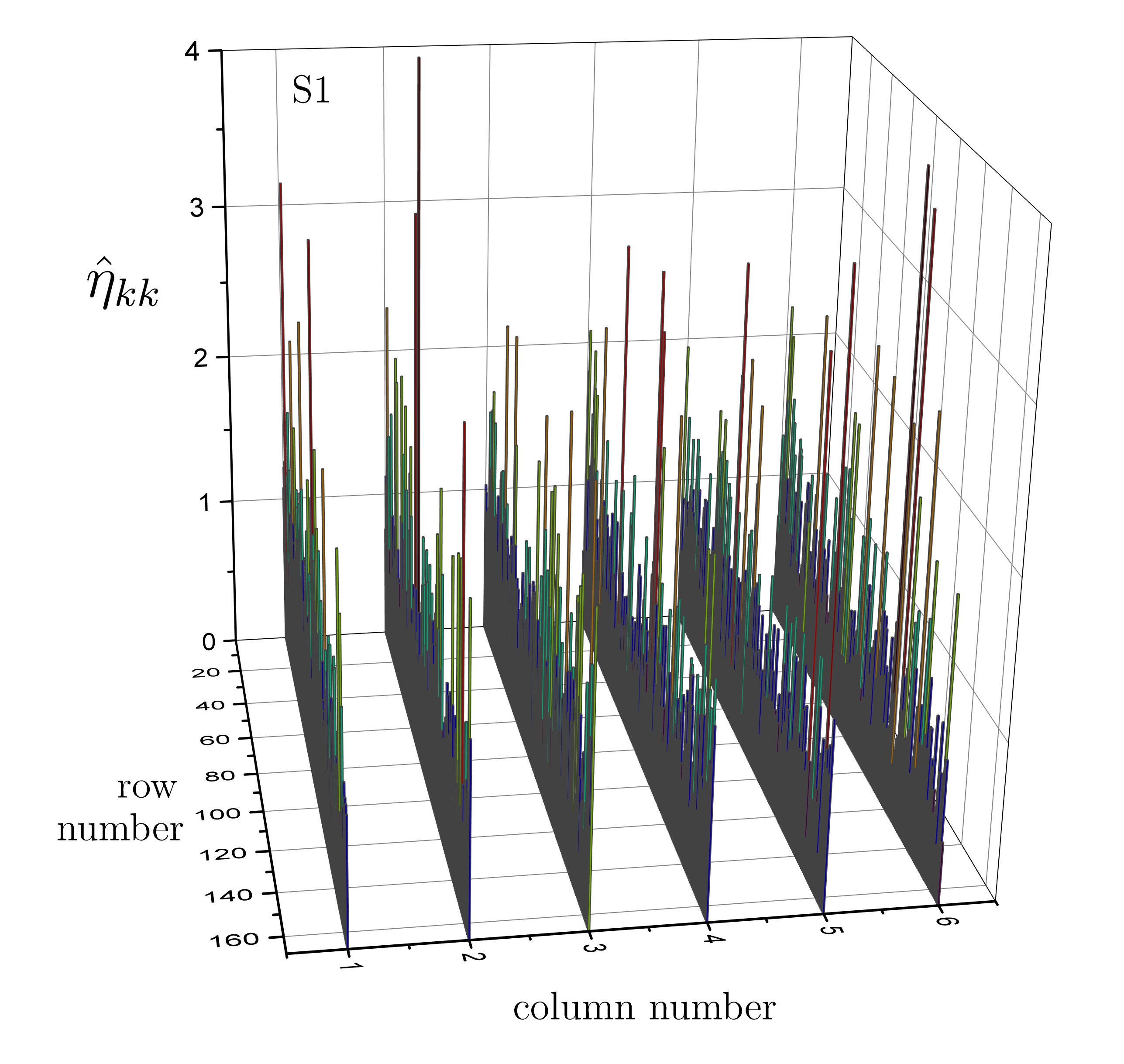
The critical currents of YBCO step-edge junctions have a spread in values and previous measurements have found wide -distributions of approximately Gaussian or even log-normal [15] shape. Therefore, when solving Eq. (16), we treat the matrix elements as log-normal random variables. A log-normal distribution with mean value 1 and standard deviation has the form
| (31) |
Here and . A log-normal distribution is similar to a Gaussian distribution for small . In our modeling, we cannot use Gaussian random variables for because they would lead to unphysical negative values, particularly for large . In the following we call the standard deviation the -spread.
The number of unknown parameters is reduced slightly further by the relation between the measured total resistance (Table II) and the unknown average JJ resistance . This relation is given by
| (32) |
Here the symbol means that the indices (where to is the row index and to , the column index) are mapped onto the index which runs from 1 to . For arrays with sufficiently large , due to the introduction of and Eq. (32), one no longer is dealing with parameters but instead one only has to deal with three parameters, which are , and . Because S1 and S2 were produced from the same YBCO thin film on the same substrate, one can expect and to be the same for S1 and S2. But because of the finite values and , one can expect a slight difference between the average values of array S1 and S2. The values of , and for S1 and S2, that were found to best model our experimental data, are listed in Table III. These values were found by probing many different , and combinations and comparing by eye the calculated and curves with the experimental data curves. The search for the , and parameters was made easier by exploiting the facts that the curves are very sensitive to and that decreasing shifts upwards and increases the voltage modulation depth , whereas increasing only decreases . Because of the -disorder and the finite size of the arrays, the parameters , and can only be determined with our procedure with some uncertainties which we estimated to be about 2%, 5% and 10%, respectively. Previously, in DC-SQUIDs [23] that were made from similar YBCO thin films, a value of m was found, which is close to m used here.
| # | [A] | [m] | [m] |
|---|---|---|---|
| S1 | 19.3 | 0.42 | 0.5 |
| S2 | 20.2 | 0.42 | 0.5 |
While doing the calculations we found that the inductance matrix elements between rows are quite small because the superconducting busbars sufficiently separate the holes of adjacent 1D parallel SQIF arrays (rows). We noticed that neglecting the small row-row mutual inductances made no noticeable difference to any of our results. Therefore, our 2D arrays behave like independent 1D parallel SQIF arrays where the 2D array DC voltage is simply the sum over all the row DC voltages. Being allowed to neglect the row-row coupling simplifies Eq. (16) and dramatically reduced the computational time needed to calculate the time evolution of the JJ phases.
Though each of our 2D SQIF arrays contains JJs, is still not large enough for and to become independent of the chosen -disorder set {}. We have investigated 40 different randomly chosen sets {} for both S1 and S2, and selected the two -disorder sets that fitted our S1 and S2 experimental data best.
Figure 5 shows calculated characteristics for S1 and S2, using the parameters in Table III, for 10 different randomly chosen -disorder sets {} for each array. The curves vary, as each -disorder set {} produces a somewhat different result. Figure 6 displays the -disorder set {} used to calculate the dotted characteristics of S1 in Fig. 5. Due to the long tail of a log-normal distribution with , values of as large as 4 can be seen.
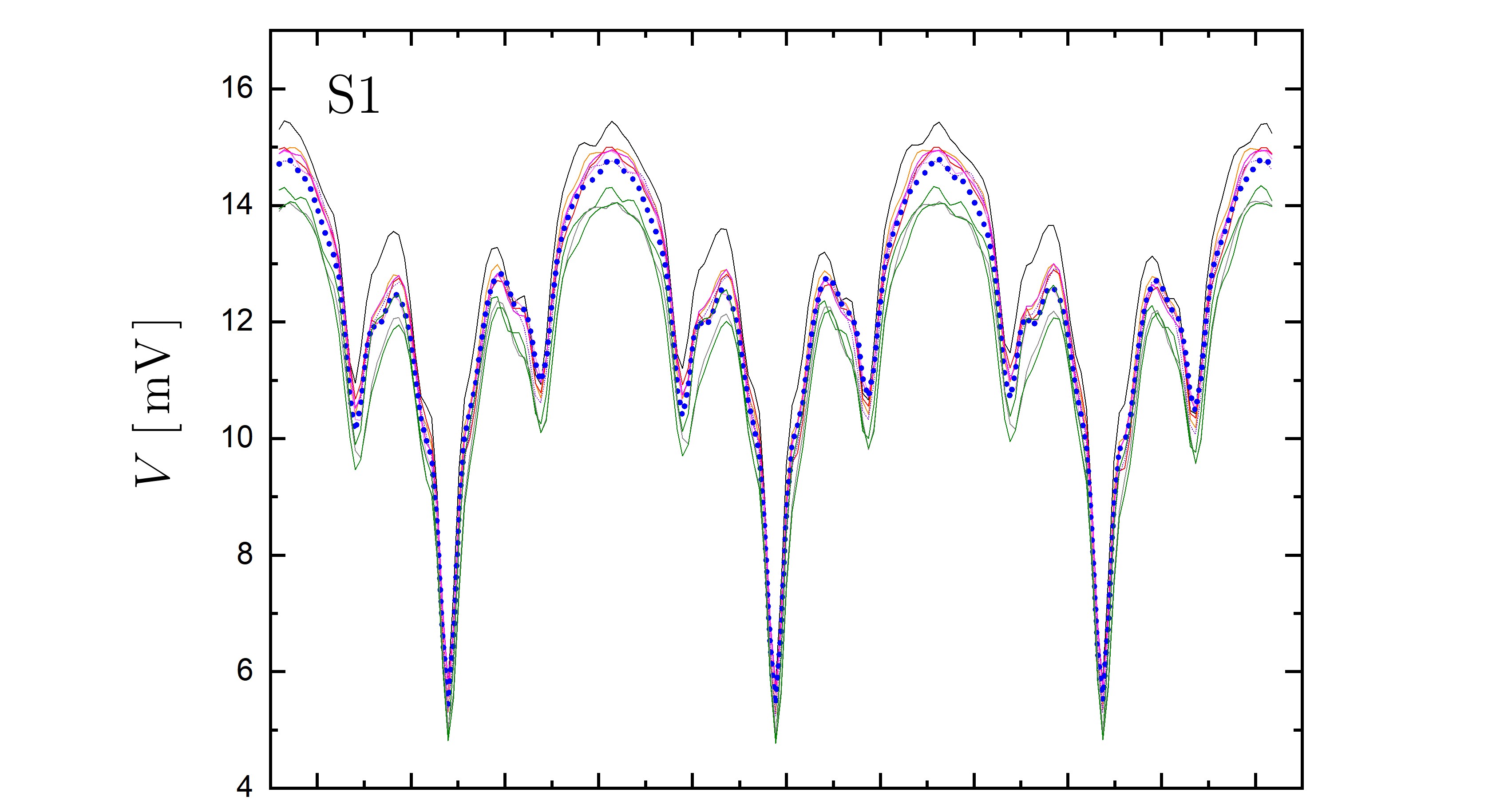
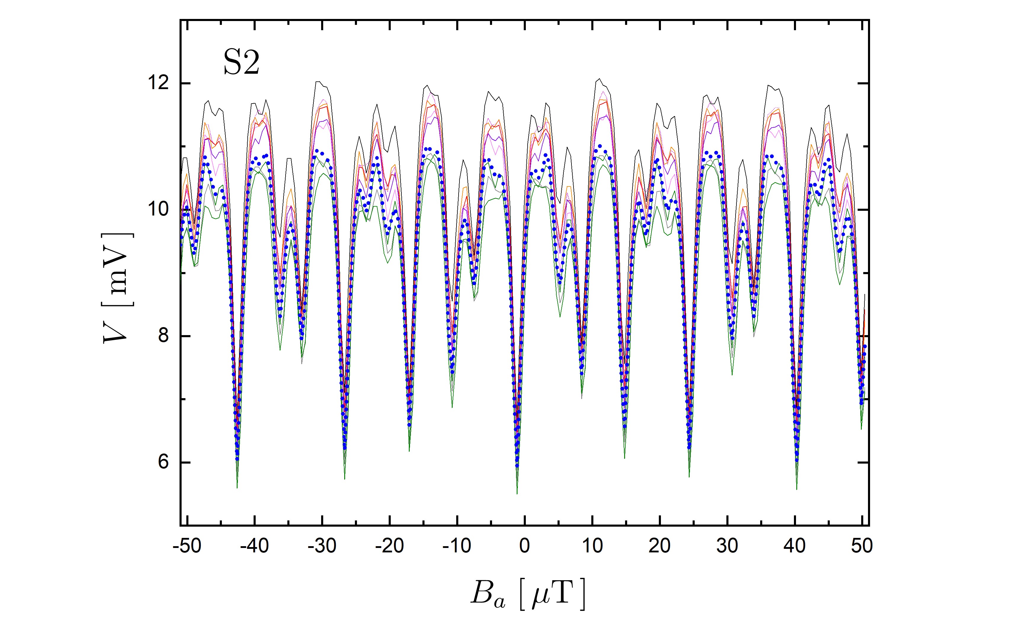
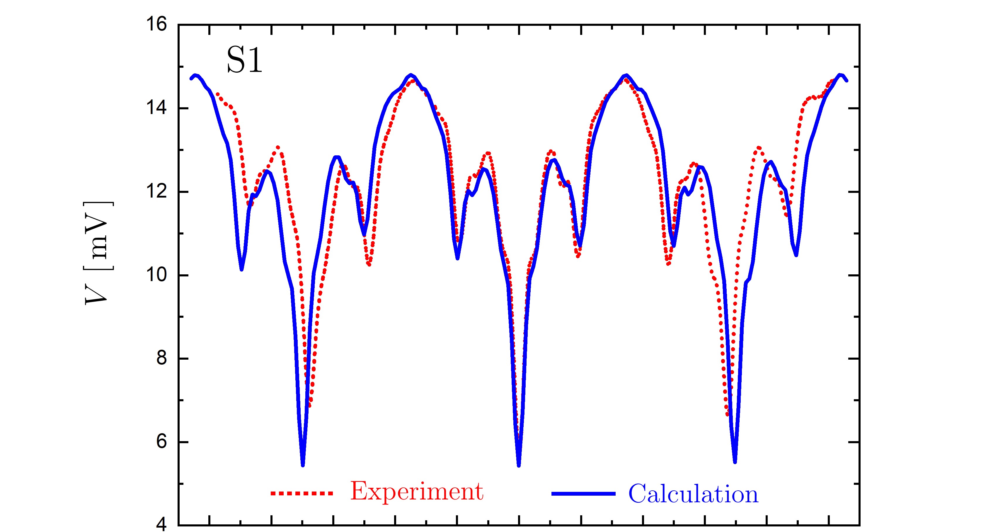
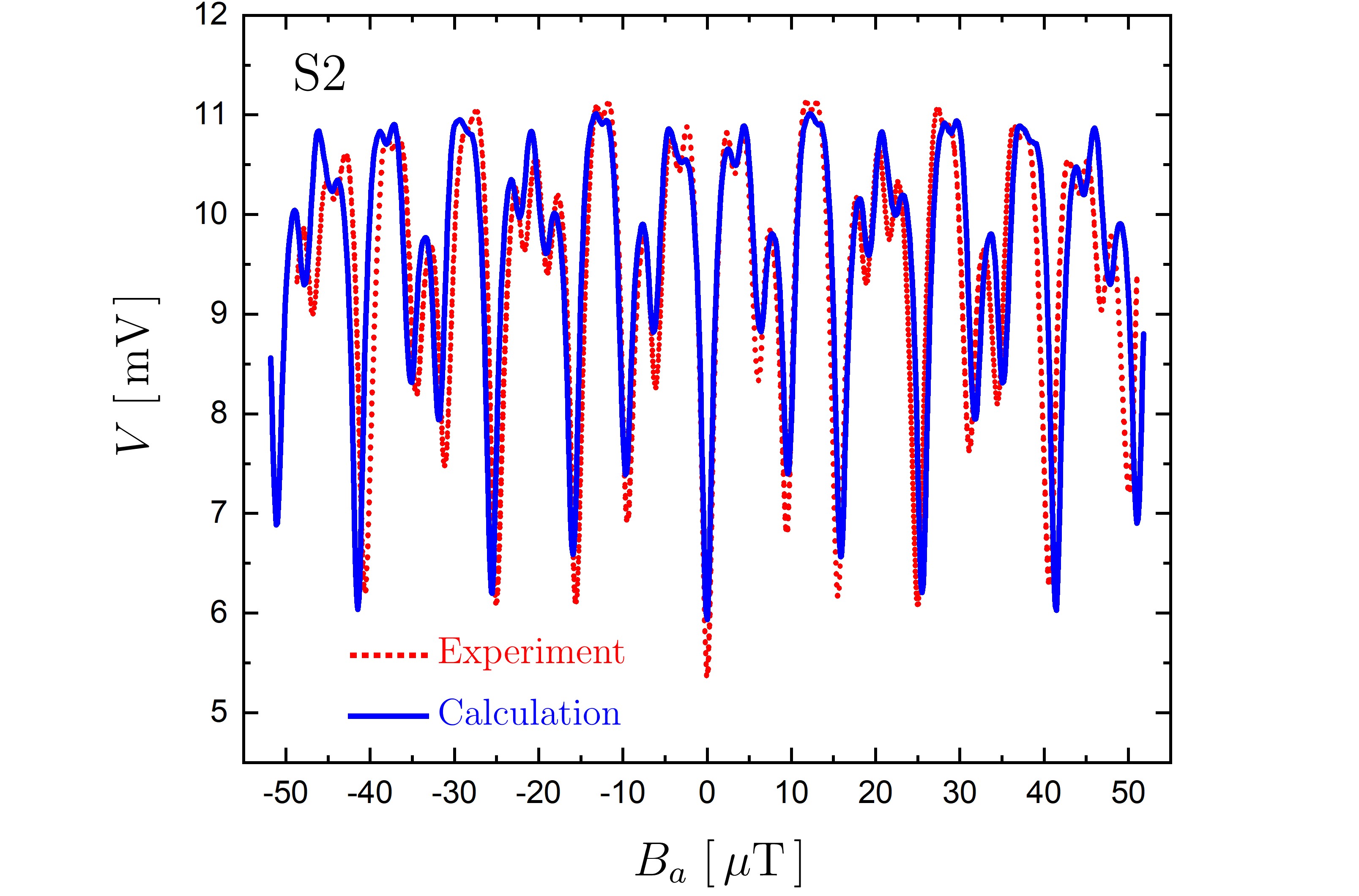
The calculated dotted curves from Fig. 5 for S1 and S2, together with our experimental S1 and S2 data from Fig. 2, are displayed in Fig. 7. Figure 7 shows a key result of our paper. The quantitative agreements between experimental data and calculation for both S1 and S2 are exceptional. Still, we could have improved the agreement even further by searching for more optimal -disorder sets {} . It turns out that the effective hole areas are important ingredients to describe the experimental data correctly. As can be seen in Fig. 7, the calculated curves are slightly more stretched along the axis than the experimental data. After the calculation, we found out that this discrepancy can be partially explained by the fact that the layout size of the arrays was actually about 2% larger than the values given in Table I. Furthermore, our calculations showed that the term in Eq. (16) which contains the bias current inductance can be neglected without affecting our calculated characteristics.
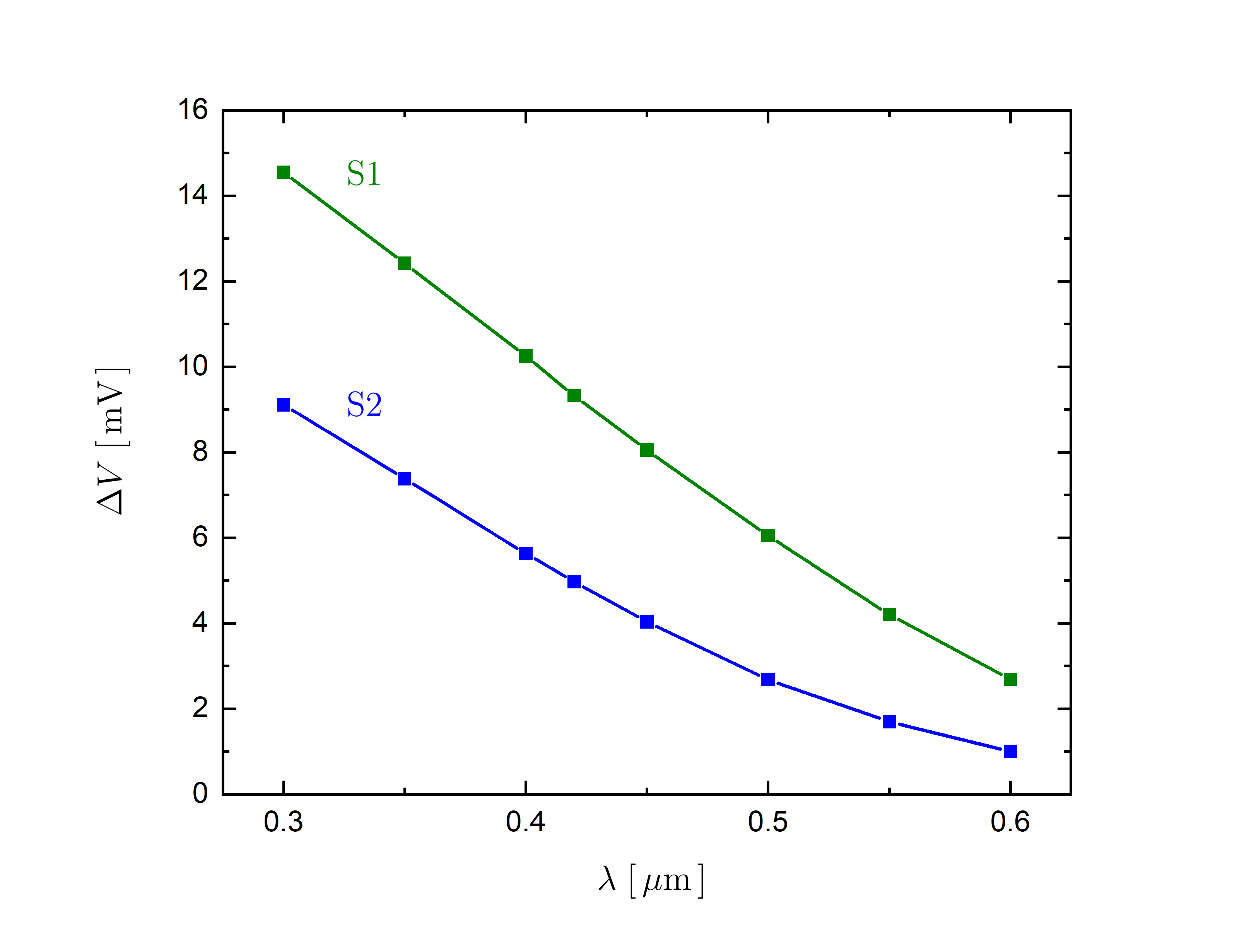
To gain a better understanding of the role of the London penetration depth , Fig. 8 shows, for S1 and S2, how (for positive ) changes with while all other parameters stay unchanged. Increasing causes the voltage modulation depth to decrease. This is mainly due to the increase in the kinetic inductances which are proportional to . This is similar to a DC-SQUID where an increase of the screening parameter leads to a decrease of [24].
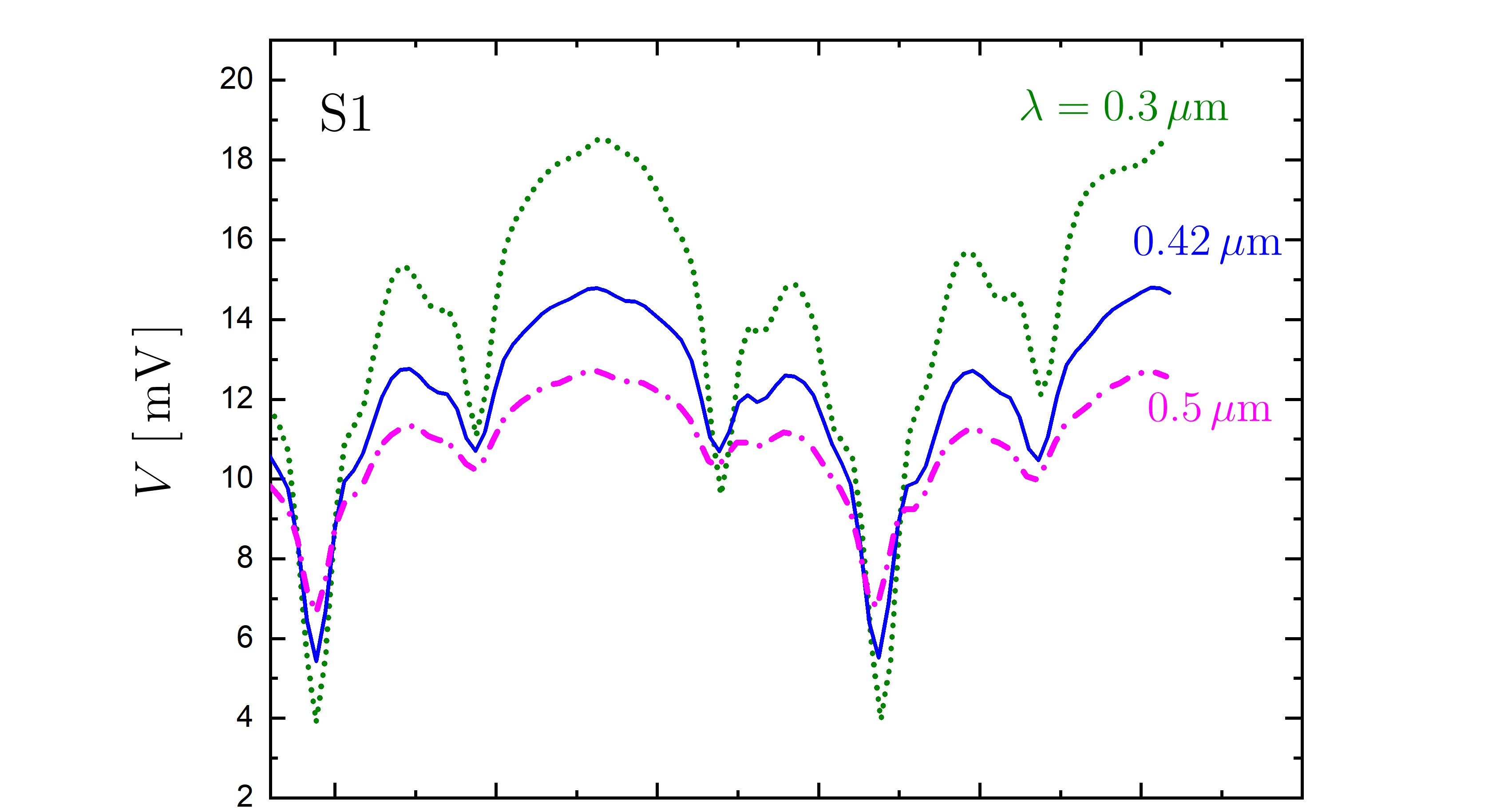
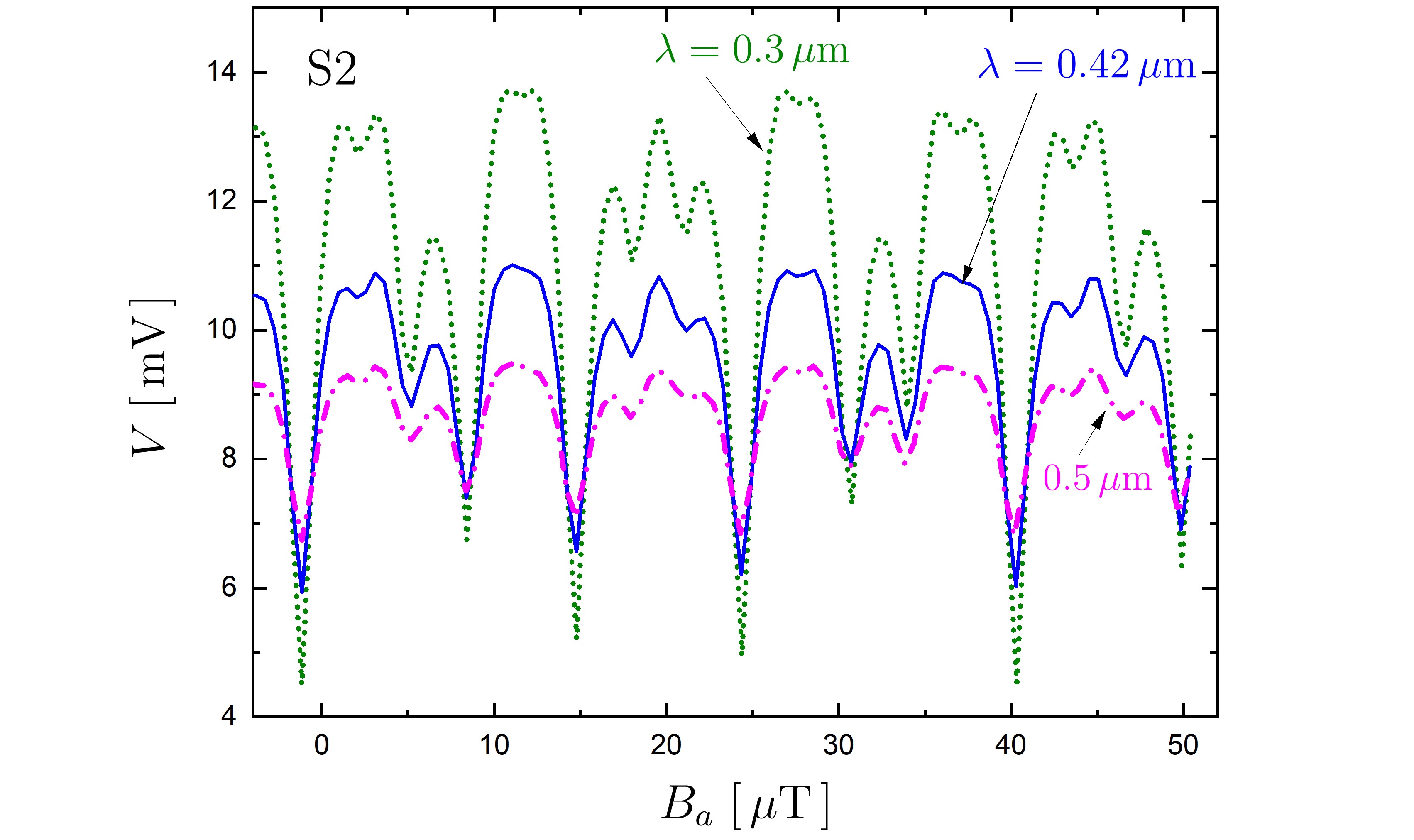
Figure 9 shows how rapidly the voltage modulation depth for S1 and S2, which is a measure of the maximum transfer function [8], decreases with increasing . Note that enters our calculations via the factor (Eq. (24), and Eq. (30) with Eq. (5)), which is known as the Pearl penetration depth [25]. Thus, increasing the film thickness , as long as [21, 18], would further increase the modulation depth of our arrays, assuming that all other parameters stay unchanged. Figure 10 shows, for S1 and S2, how the characteristics (for positive ) change with the -spread while all other parameters stay unchanged. Increasing smoothes the curves, which decreases the voltage modulation depth . The underlying cause
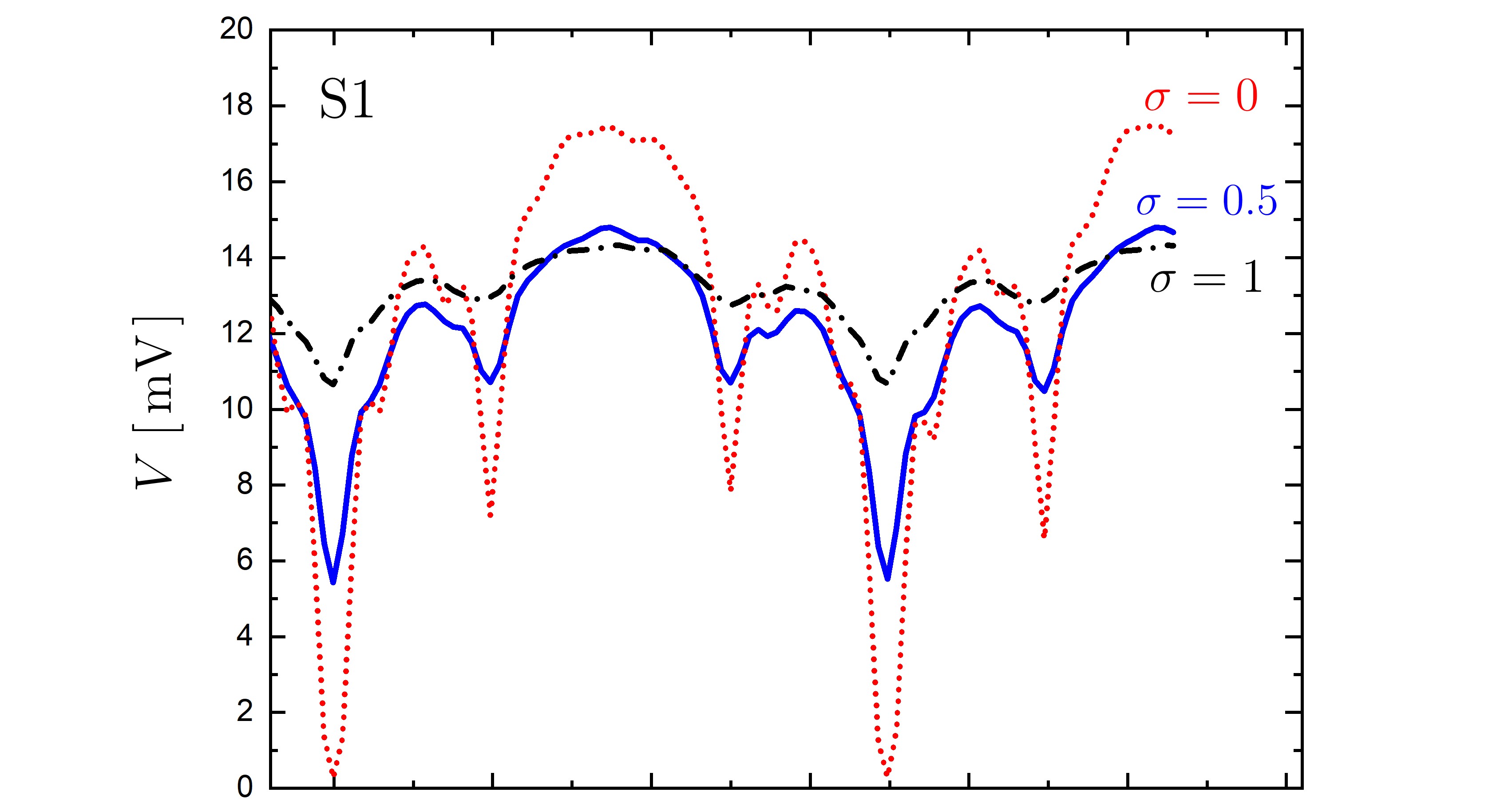
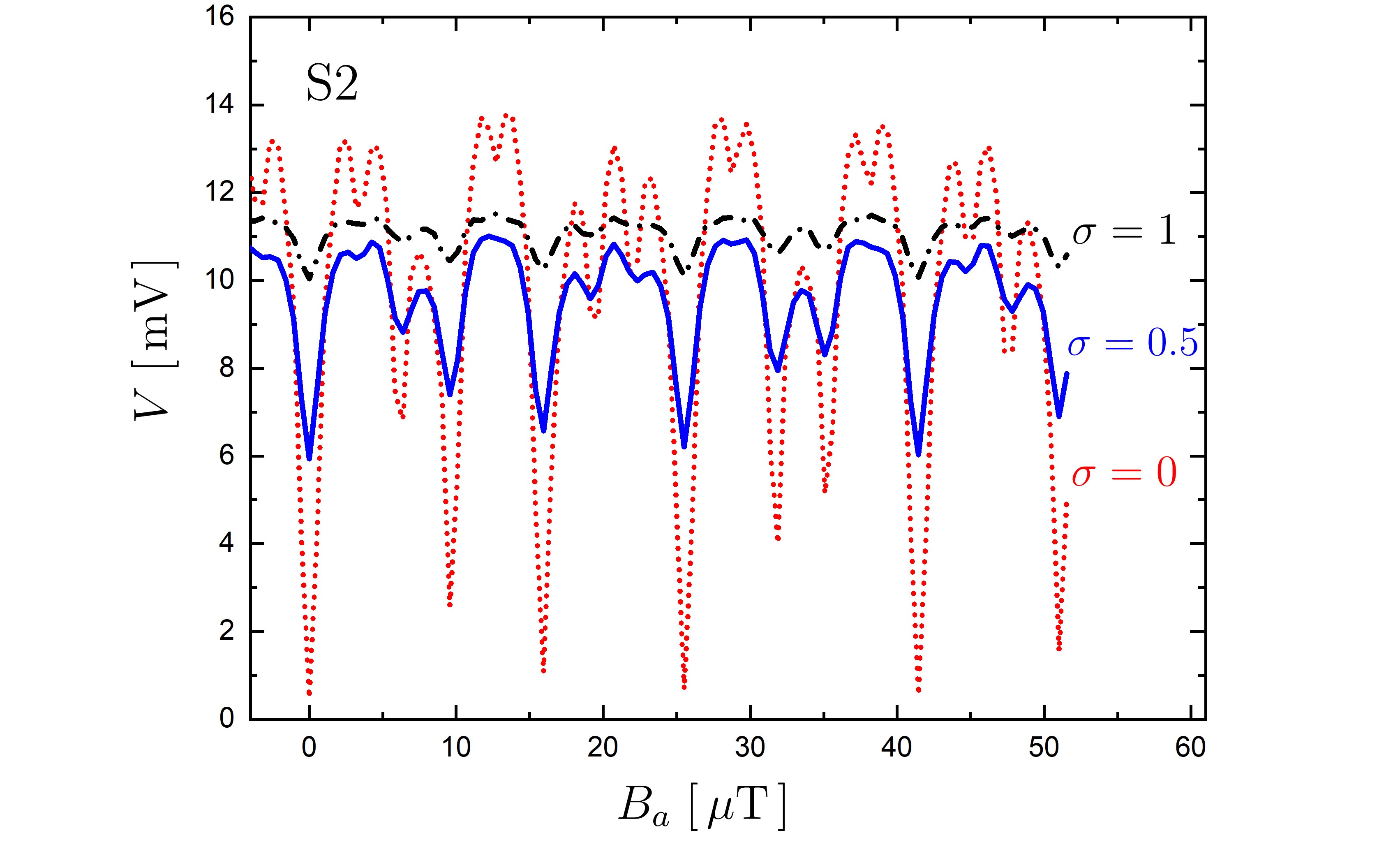
is revealed by looking at the characteristics of the simple DC-SQUID () with and [24, 26]. Here, the -asymmetry causes a skewing of the response [24] and the -asymmetry a -shifting to the left or right by an amount where is the self-inductance of the DC-SQUID loop [26]. In addition to the reflection symmetry breaking, the modulation depth decreases with increasing -asymmetry [24, 26]. The modulation depth is less affected by the -asymmetry. In our 2D SQIF arrays each row has 6 JJ’s in parallel and 5 holes. As the ’s and ’s are all different, this produces in each row a different reflection asymmetry, i.e. , due to different skewing and -shifting. Because of the very weak inductive coupling between rows, as mentioned above, the time averaged voltages across rows can simply be added up to give the total array voltage . Adding up a large number of different row voltages causes a smoothing which reduces the modulation depth of the array but also reduces the reflection asymmetry.
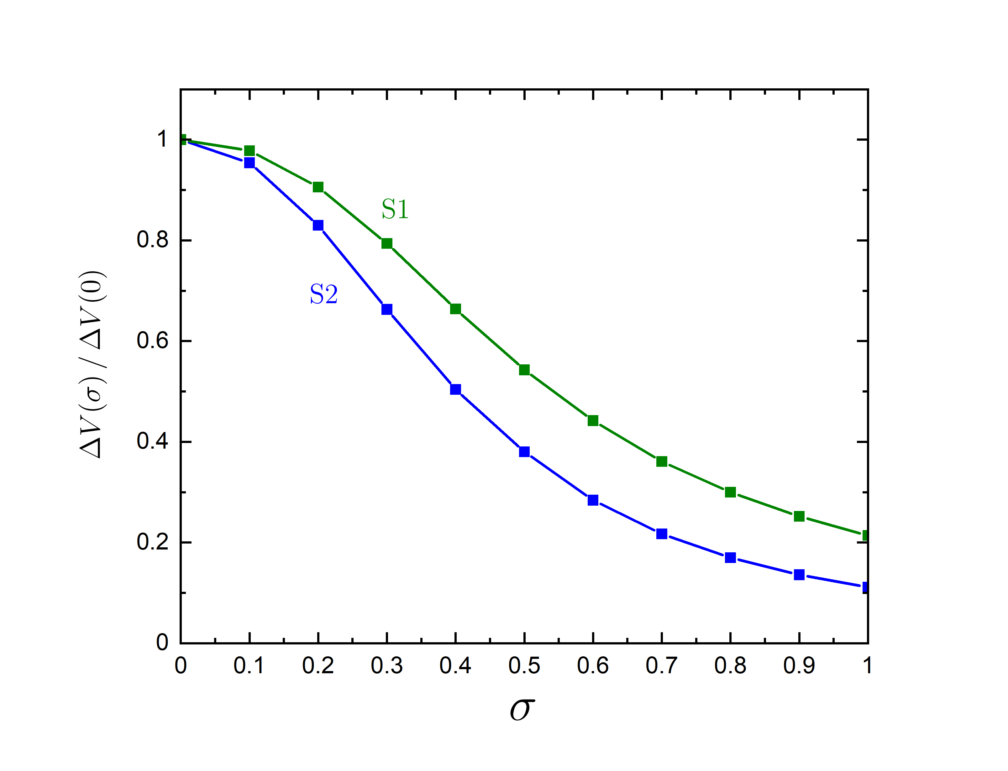
Figure 11 displays normalized by . The figure shows that an -spread reduces in the case of S1 from 1 to about 0.55 and in the case of S2 from 1 to about 0.4. Figure 11 reveals that --disorder has a stronger detrimental effect on in an array with larger inductances like S2 than in an array with smaller inductances like S1. Figure 11 is one of the key results of this paper.
In Appendix D we discuss the weak reflection asymmetry of .
Figure 12 shows the experimental and calculated characteristics in zero applied magnetic field for S1 an S2. The calculation does not perfectly reproduce the experimentally observed at low . Better agreement can possibly be achieved by modifying the log-normal distribution in Eq. (31) such that low values become more emphasized. The values of for S1 and S2 are indicated in Fig 12. In contrast to , the calculated shape of is not very sensitive to a particular choice of the -disorder set {} for a given , but is very sensitive to the choice of , i.e. the average value.
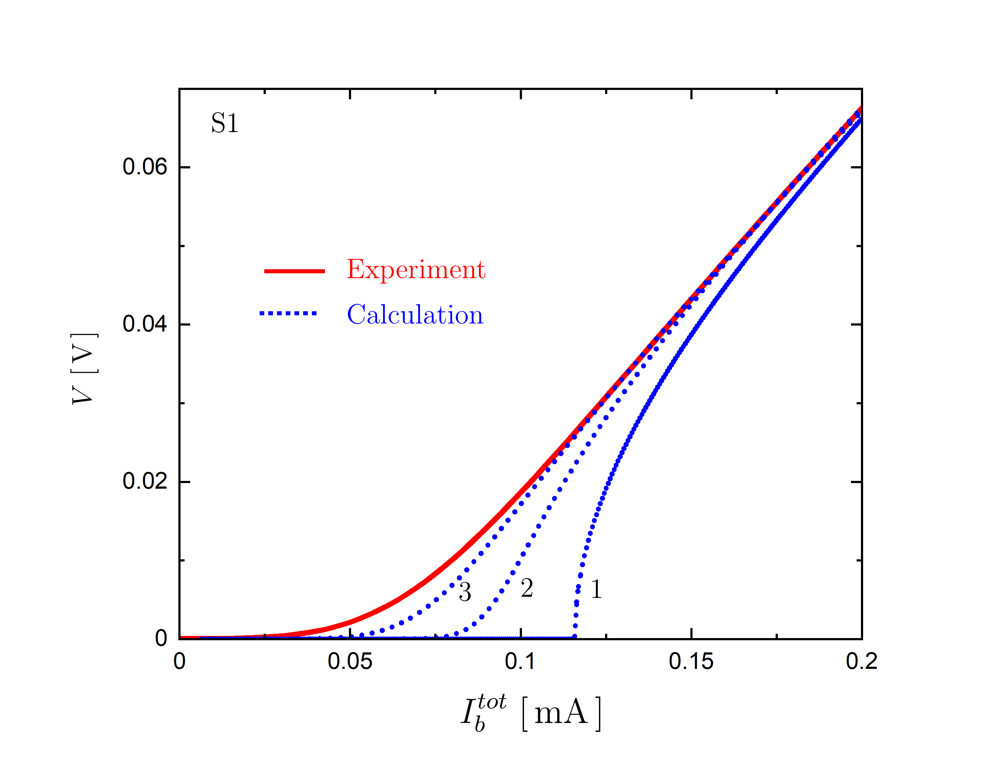
Figure 13 again displays for S1 but here the calculated additional dotted curves reveal how the parameters and affect the shape of . Going from curve (1) to (2) shows the effect of temperature K, and going from (2) to (3) the effect of .
VI Summary and Conclusion
We measured the characteristics at optimal bias currents and the characteristics at of two 2D SQIF arrays with and .
To model our experimental data, we developed a theoretical model that takes into account the Johnson noise in the JJ resistances , the spreads in and , and the wide, thin-film busbar structure of the arrays. The model was made numerically efficient by dividing the superconducting current density into its Meissner current, circulating current, and bias current parts. Using the stream function approach for , we calculated the effective areas of the array holes, inductance matrices and bias current inductance vectors. The calculations revealed that the busbar height was sufficiently large such that the inductive row-row coupling could be neglected. This significantly simplified the numerical calculations and made the investigation of the --disorder of our arrays computationally possible.
Empirical findings that can be expressed in terms of reduced the parameter space, and we could identify sets from a log-normal distribution that produced characteristics that agreed well with our experimental data.
Our calculations demonstrated that the voltage modulation depth , which is a measure for the maximum transfer function, decreases with increasing due to the increase in kinetic inductances which are proportional to .
Most of all, our calculations showed how decreases with increasing -spread , where the decrease was more rapid for the high inductance array S2. Our experimental data were best described by , showing that the --disorder in our arrays reduced by 45% in S1 and 60% in S2.
We observed slight reflection asymmetries in our experimental characteristics, caused by the --disorder, and our model predicted a similar degree of asymmetry as observed experimentally. Generally, the refection asymmetry increases with increasing -spread , but decreases when is increased.
The calculated characteristics did not fully agree with our experimental data at low , possibly due to the choice of a log-normal distribution that did not sufficiently emphasize low values. Modifying our log-normal distribution would give better agreement with without affecting much the results. Our calculations also showed how the characteristic changes with temperature ( to K) and with ( to ).
Our findings suggest that the use of YBCO thin films in SQIF arrays is promising, as the critical current disorder inherent in their fabrication process reduces the transfer function in our case only by about a factor of 2. This is one of our important results. Our study highlights the importance of theoretical modeling in understanding the performance of superconducting devices and provides insights that could inform the design of future SQIF arrays. While our detailed theoretical modeling provided valuable insight into the role of --disorder for the specific arrays tested, more general investigations are needed to fully understand its role as a function of screening parameter , noise strength , kinetic inductance fraction, and values, and different array planar geometries.
Acknowledgements.
The authors would like to thank Marc Gali Labarias for stimulating discussions.Appendix A Effective hole areas
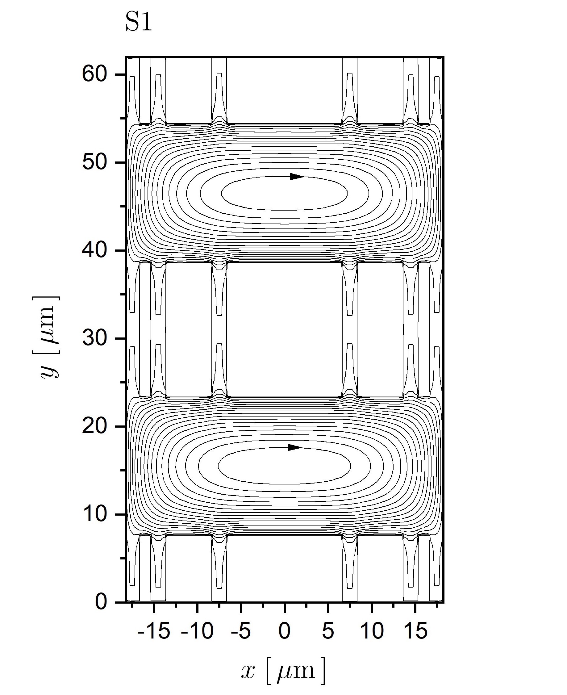
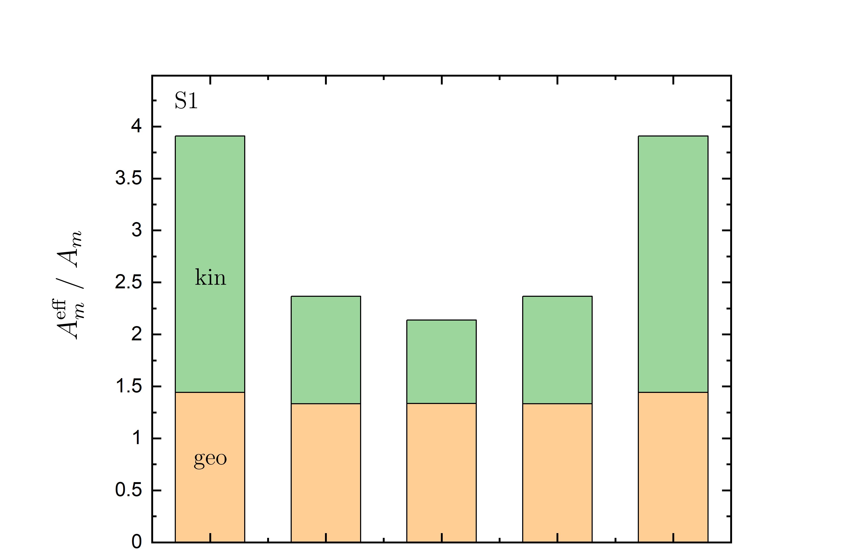
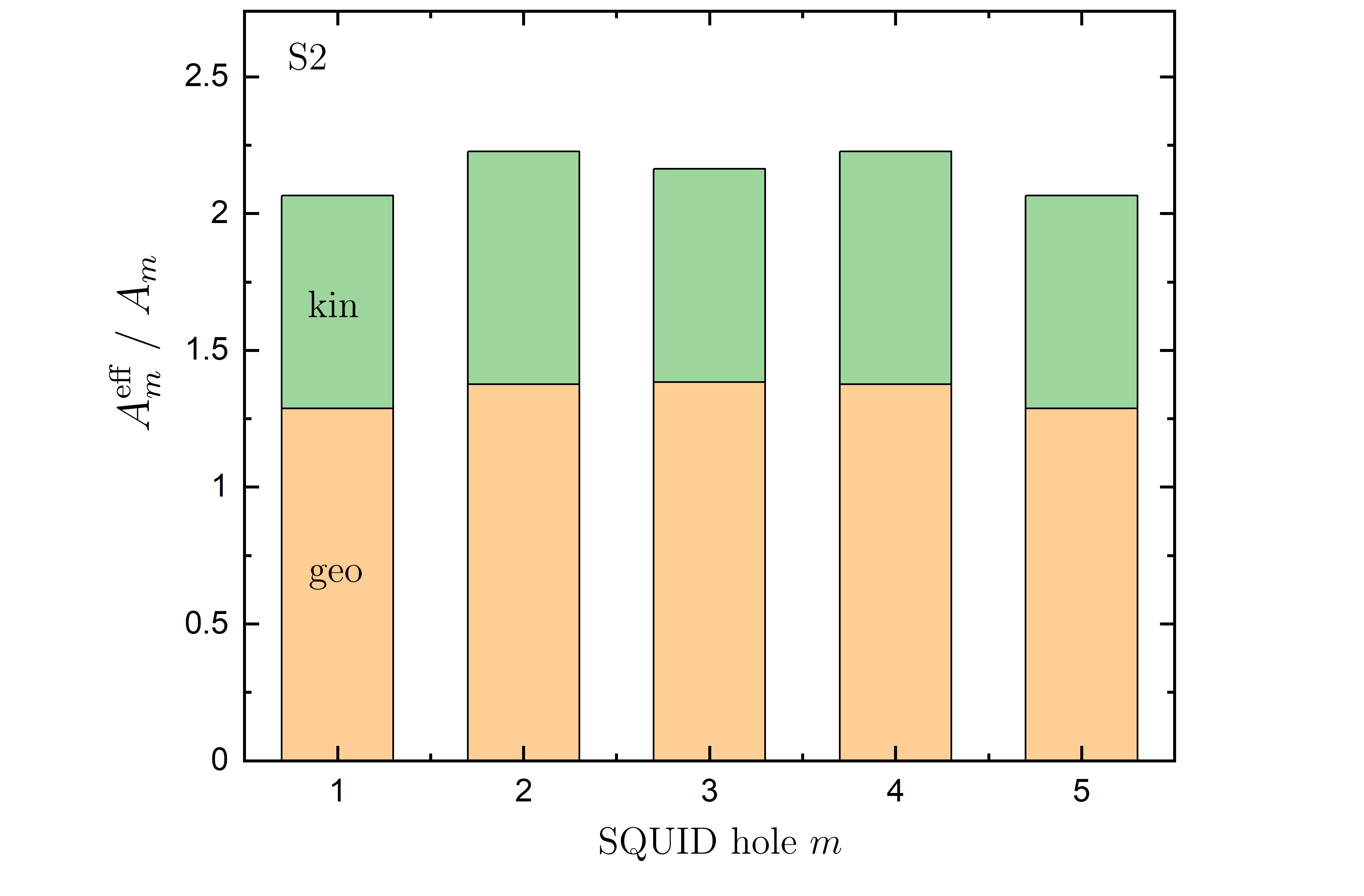
By choosing any constant applied magnetic field, , and the boundary condition , for all boundaries , one can calculate numerically, by solving Eq. (24), the part of that corresponds to the Meissner shielding current density . In this case (Eq. (25)). Stream-lines of in array S1 and S2 are shown in Fig. 14. Using Eqs. (28) and (30), the fluxoids (Eq. (9)) of the different holes are determined and the effective hole area enhancement factors (Eq. (13)) are calculated.
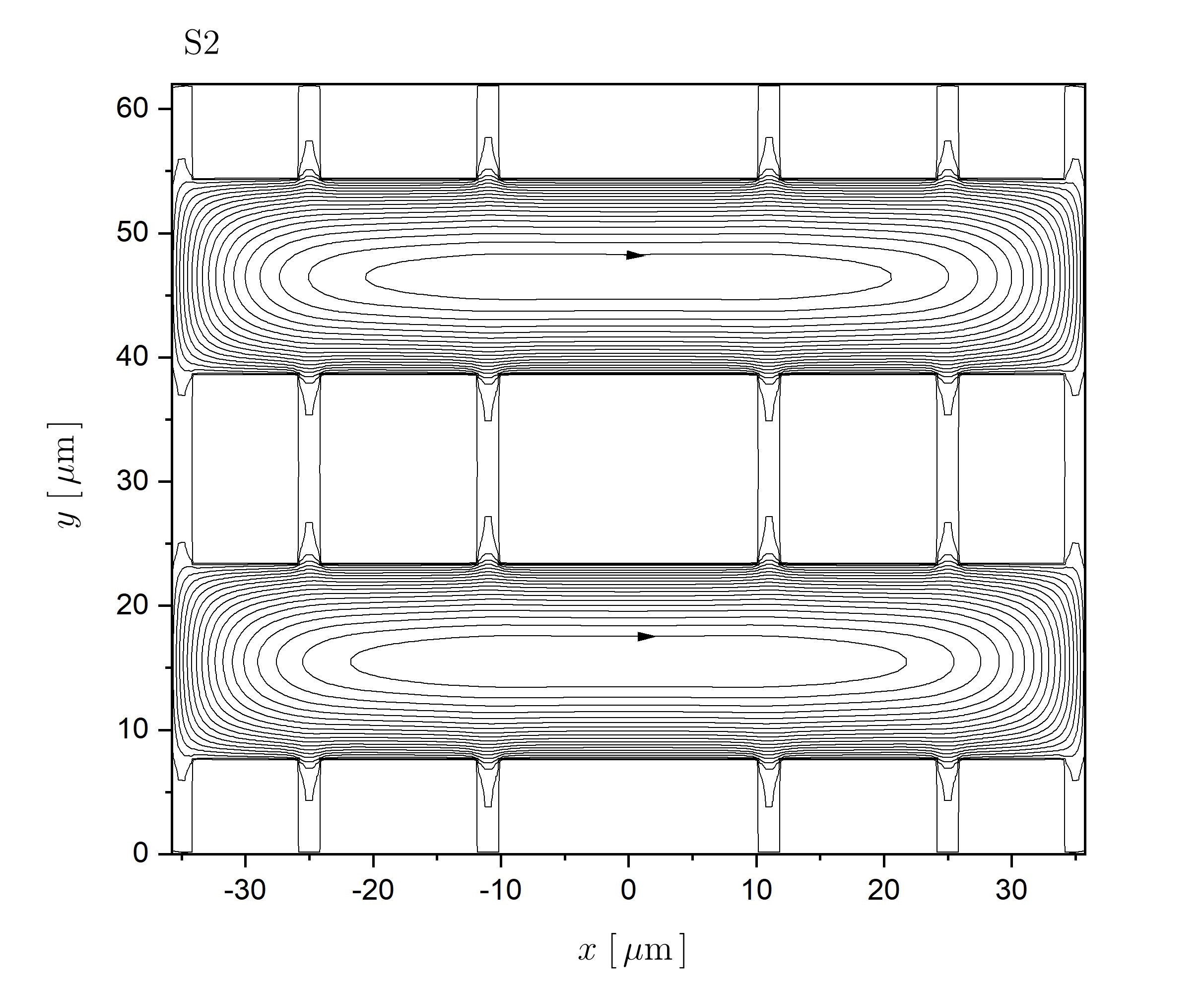
for different holes are displayed in Fig. 15, where the geometric and kinetic parts are indicated. Figure 15 shows that the kinetic part plays an important role.
Appendix B Inductance matrix
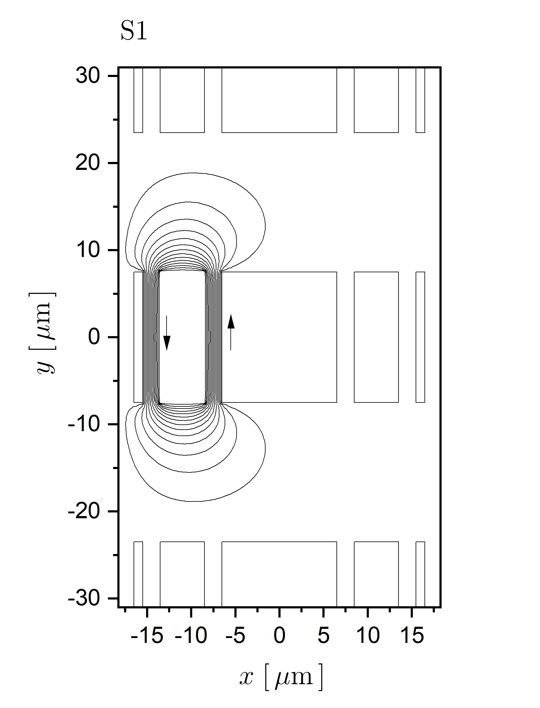
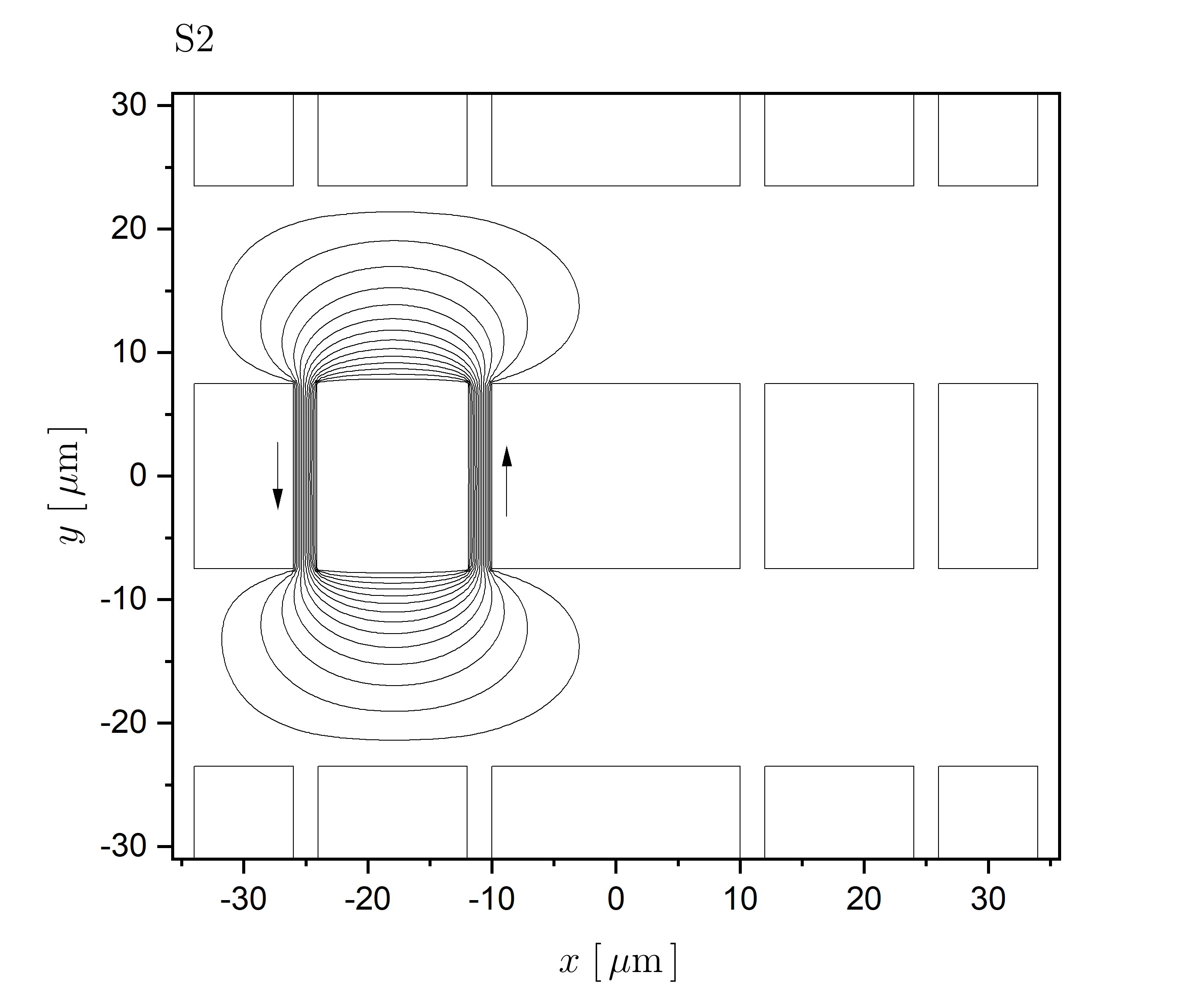
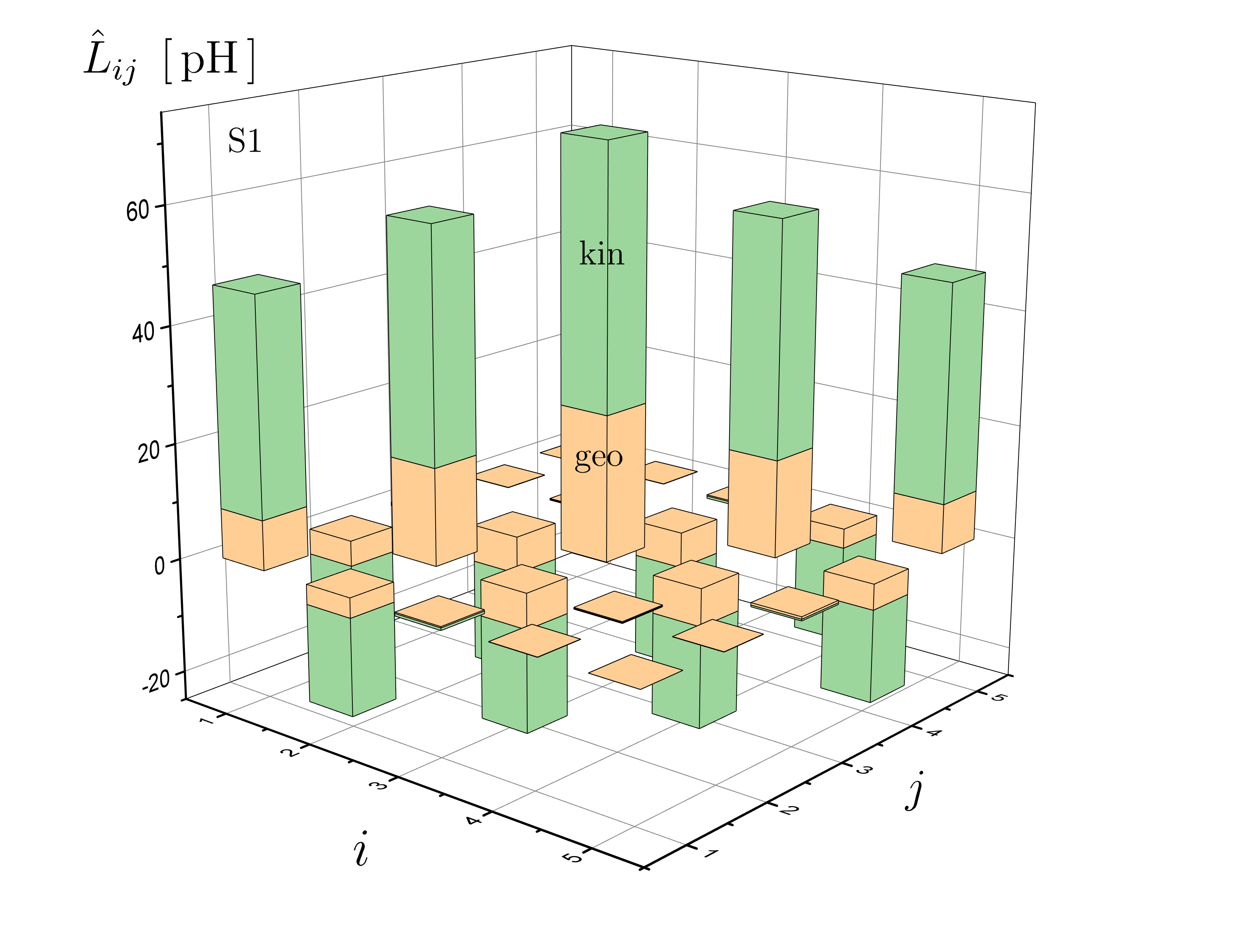
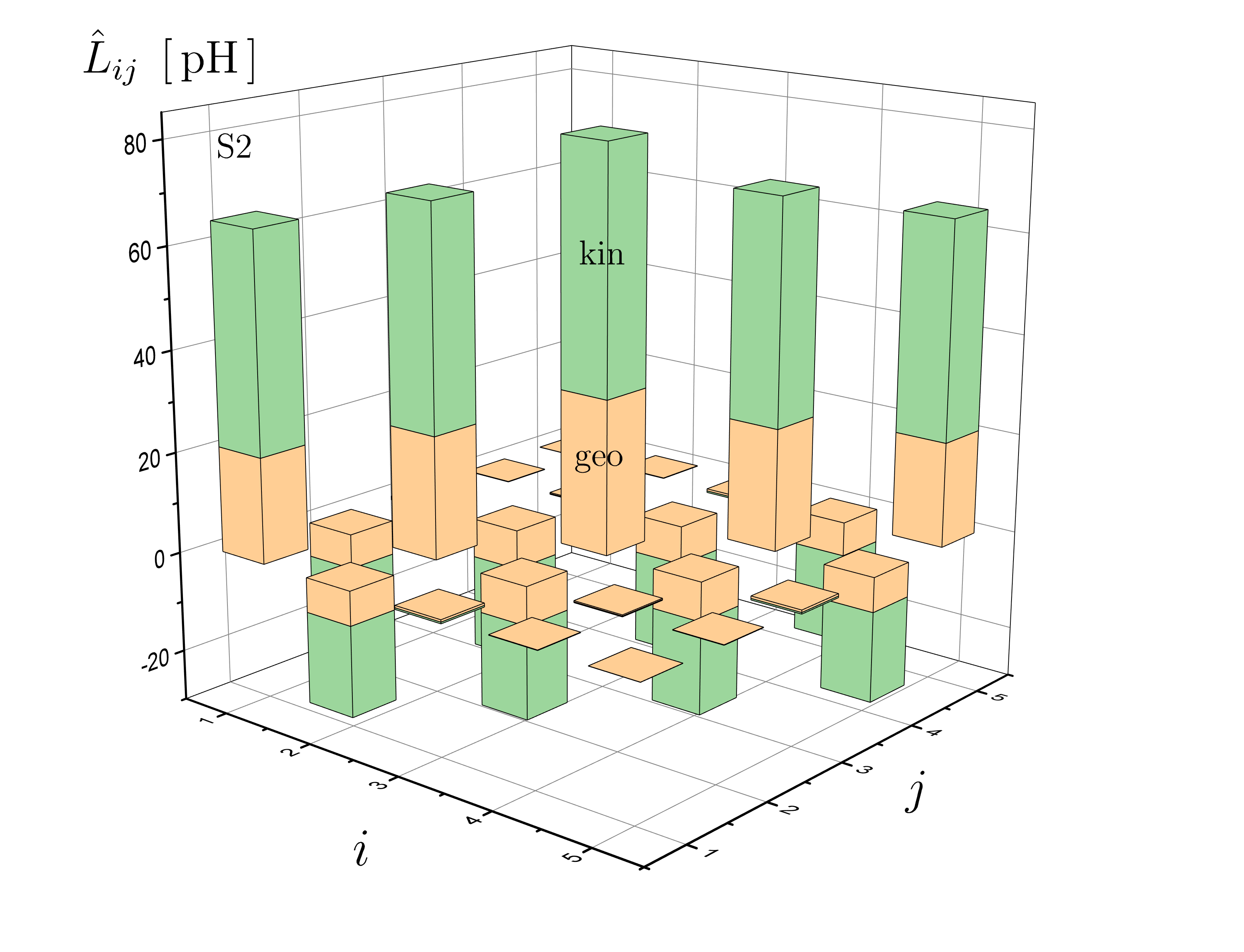
One can determine the part of , which corresponds to a counterclockwise circulating current around hole , by choosing and solving Eq. (24) numerically with the appropriate boundary condition. The boundary condition is ( but arbitrary), and increases linearly from 0 to along the left JJ and decreases linearly from to 0 along the right JJ. Everywhere else . In this case, in Eq. (25) can be obtained analytically as , where the formulas for can be found in Appendix B of ref. [1]. Examples of current stream-lines of currents flowing around a hole in S1 and S2 are shown in Fig. 16. One can use Eqs. (28) and (30) to determine the fluxoids (Eq. (10)) generated in the different holes, and then with Eq. (14) all the matrix elements of the inductance matrix are calculated. The matrix elements of S1 and S2, for the holes in a single row, are plotted in Fig. 17 and their geometric and kinetic parts are indicated. The large self-inductances are seen along the diagonal while the negative mutual inductances are off-diagonal. The row-row mutual inductance matrix elements are found to be very small and are not displayed here. Figure 17 shows that the kinetic part plays a dominant role.
Appendix C Inductance vector
One can determine the part of that corresponds to the bias transport current density by choosing and solving Eq. (24) numerically with the appropriate boundary condition. The boundary condition is along the left/right outer edges of the array, and, along the inner edges of the holes, with to , while increases linearly along the JJ’s between neighboring holes. Again, can be obtained analytically and can be expressed in terms of [1]. Streamlines of in S1 and S2 are shown in Fig. 18. Using Eqs. (28) and (30), the fluxoids (Eq. (11)) of the different holes can be determined, and with Eq. (15) the components of the inductance vector are calculated.
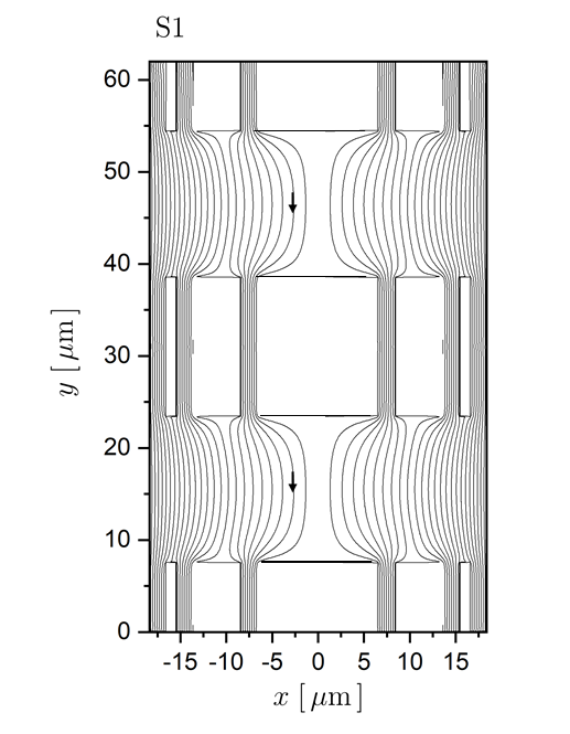
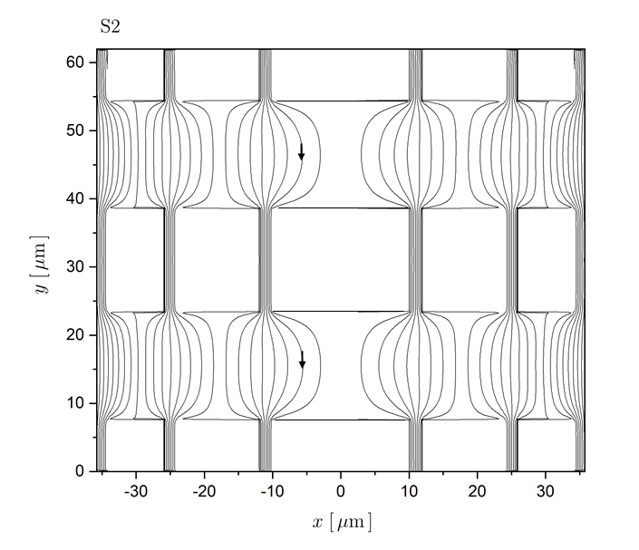
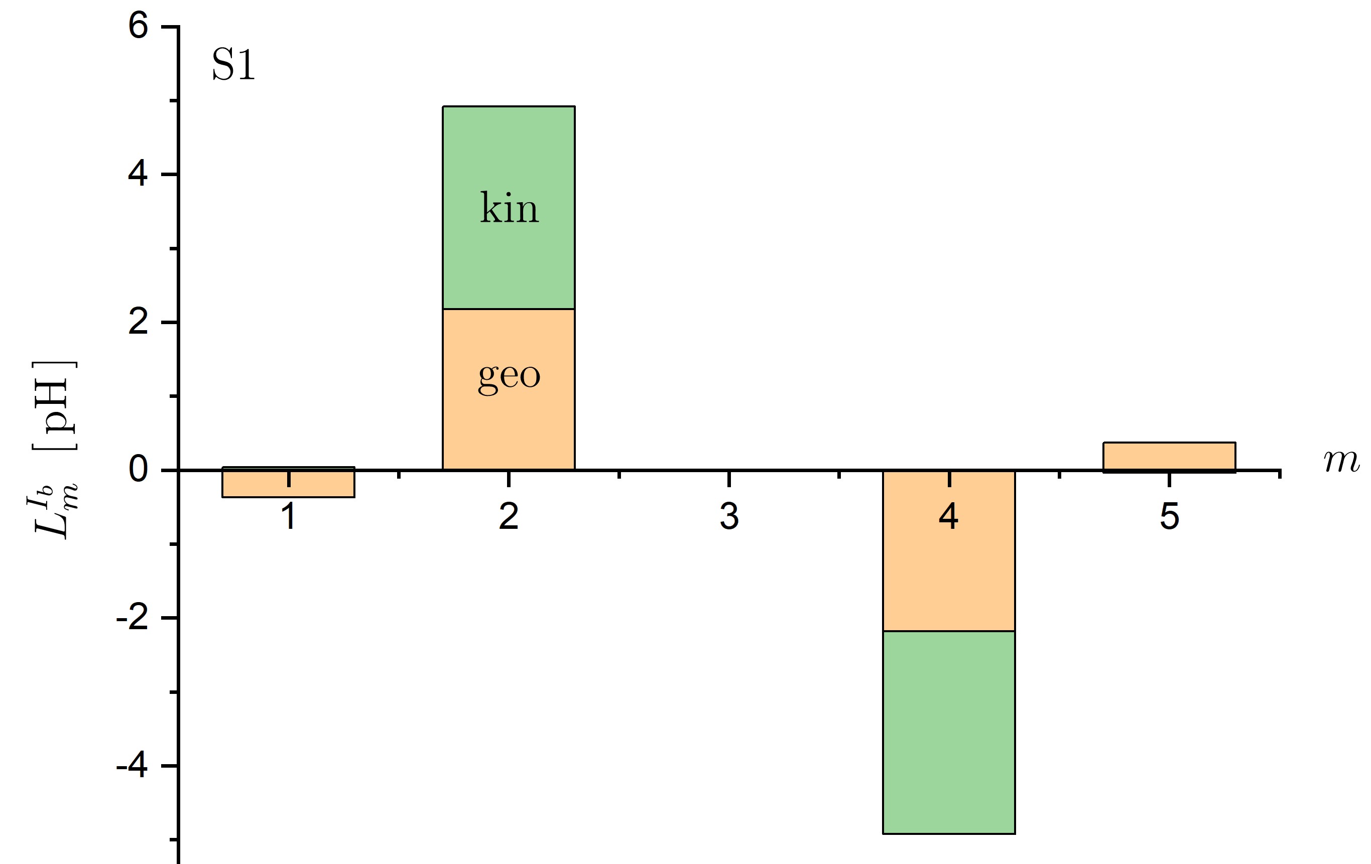
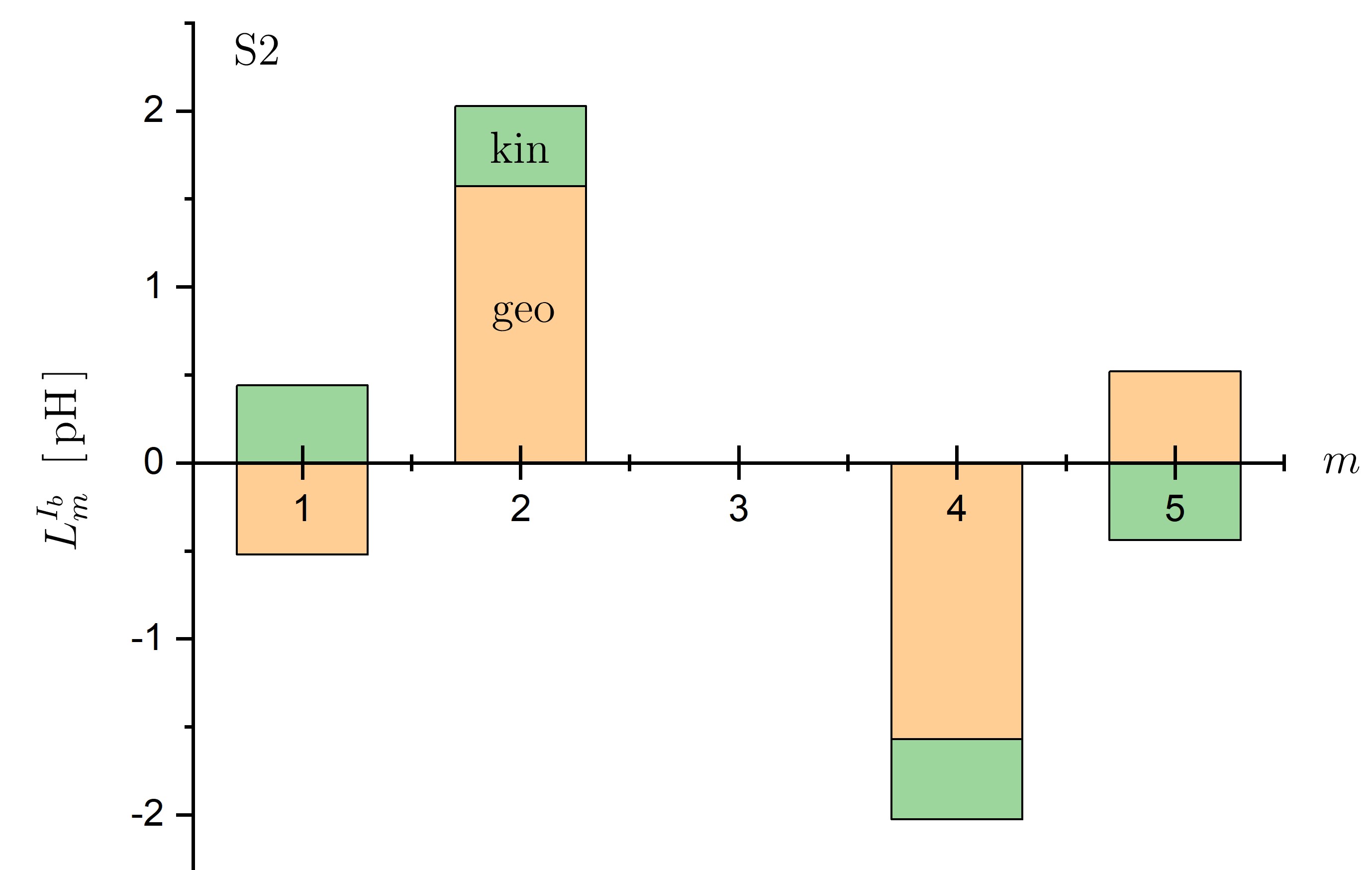
Figure 19 shows for the different holes along a row, and the geometric and kinetic parts are indicated.
Appendix D Reflection asymmetry of
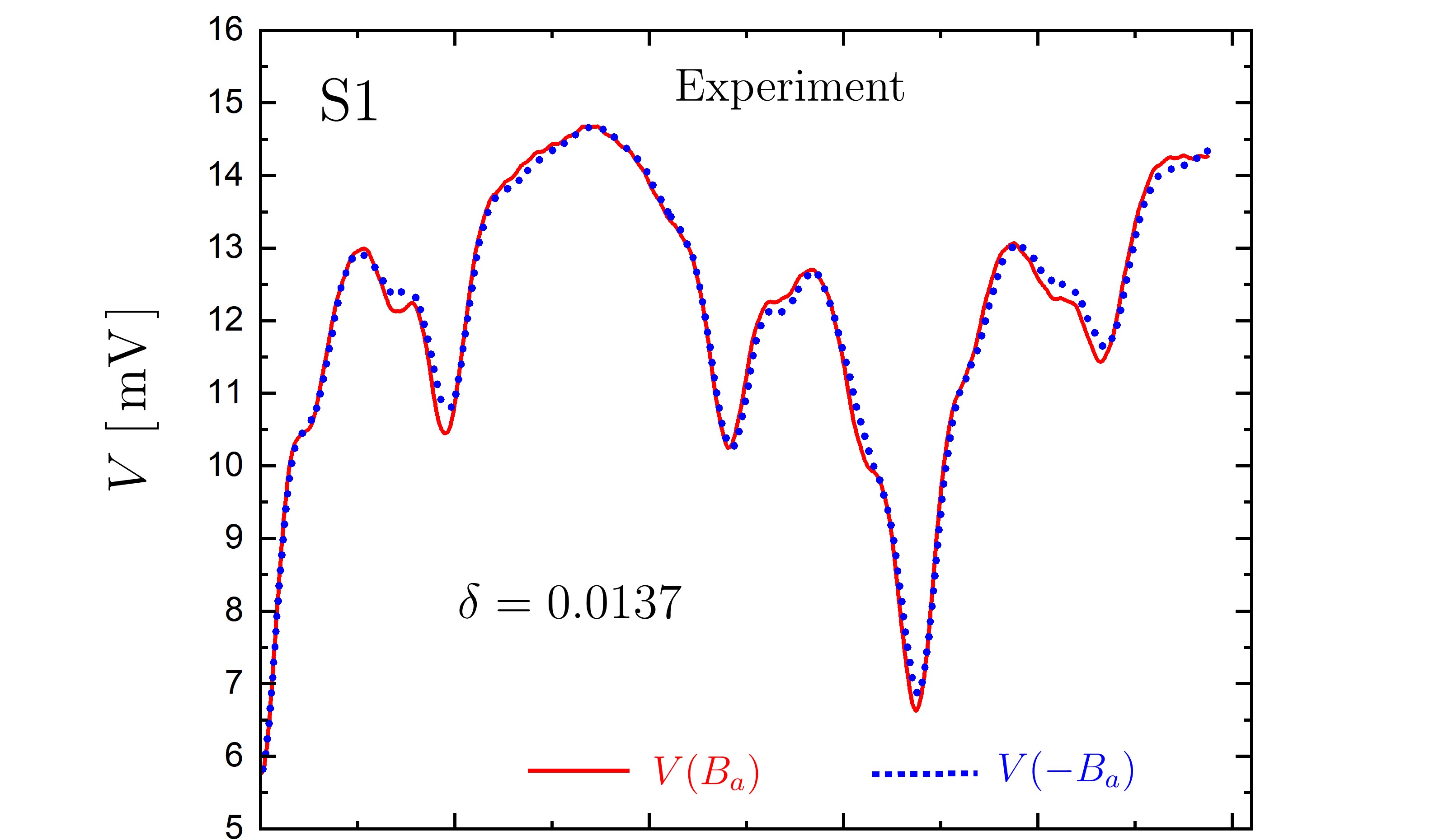
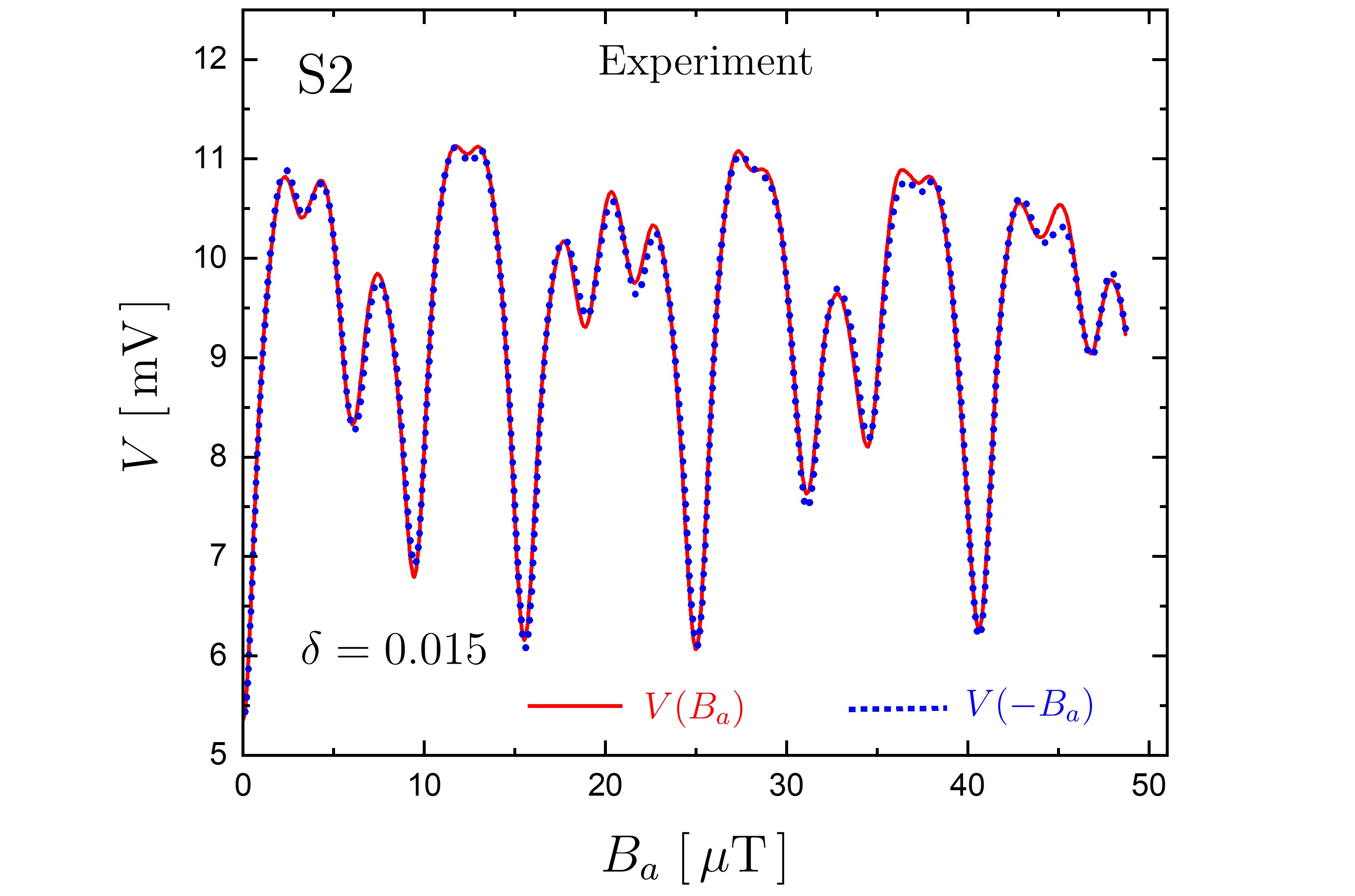
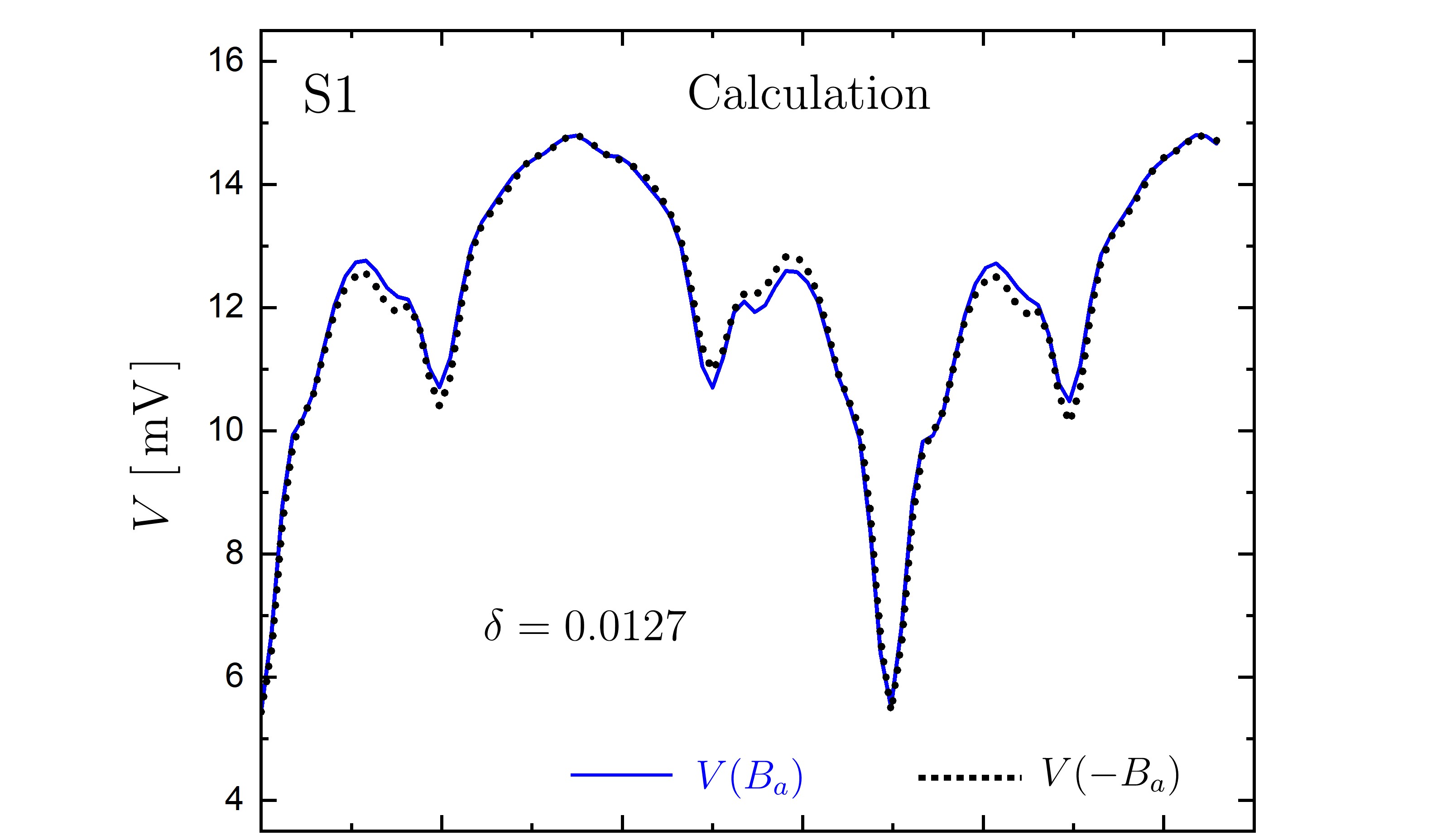
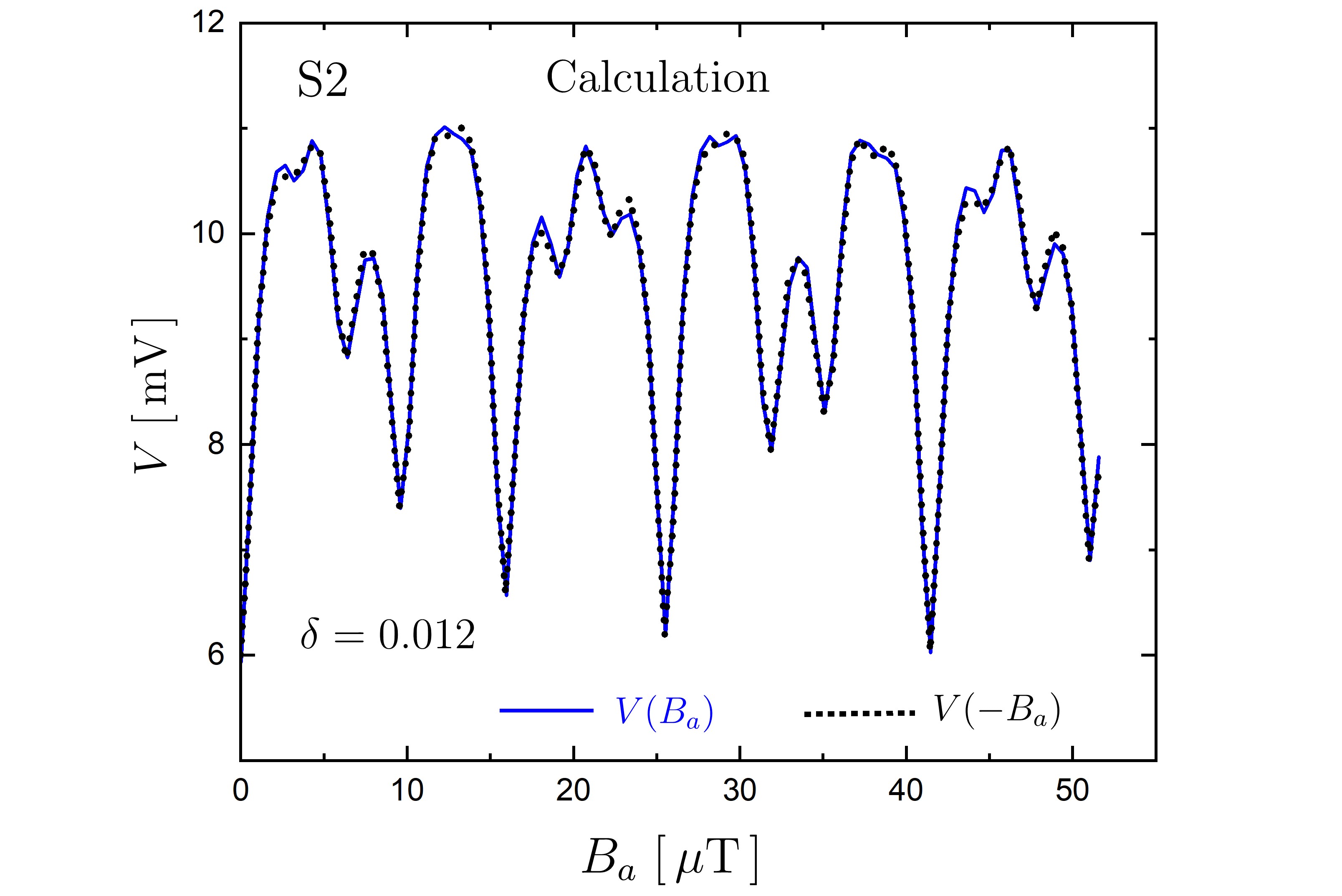
Figure 20 shows the experimental reflection asymmetry of by plotting and for S1 and S2. Small differences between and the reflected curve are noticeable. Figure 21 displays the calculated and curves. One can define the degree of the reflection asymmetry as
| (33) |
with the integration interval T. The experimental for S1 and S2 are and 0.015, respectively, while the calculated ones are and 0.012. We found from our calculations that increases when the -spread increases.
References
- Müller and Mitchell [2021] K.-H. Müller and E. E. Mitchell, Theoretical model for parallel squid arrays with fluxoid focusing, Phys. Rev. B 103, 054509 (2021).
- Cybart et al. [2012] S. A. Cybart, T. N. Dalichaouch, S. M. Wu, S. M. Anton, J. A. Drisko, J. M. Parker, B. D. Harteneck, and R. C. Dynes, Comparison of measurements and simulations of series-parallel incommensurate area superconducting quantum interference device arrays fabricated from YBa2Cu3O7-δ ion damage Josephson junctions, J. Appl. Phys. 112, 063911 (2012).
- Dalichaouch et al. [2014] T. N. Dalichaouch, S. A. Cybart, and R. C. Dynes, The effects of mutual inductances in two-dimensional arrays of Josephson junctions, Supercond. Sci. Technol. 27, 065006 (2014).
- Taylor et al. [2016] B. J. Taylor, S. A. E. Berggren, M. C. O’Brian, M. C. deAndrade, B. A. Higa, and A. M. Leese de Escobar, Characterization of large two-dimensional YBa2Cu3O7–δ SQUID arrays, Supercond. Sci. Technol. 29, 084003 (2016).
- Mitchell et al. [2019] E. E. Mitchell, K.-H. Müller, W. E. Purches, S. T. Keenan, C. J. Lewis, and C. P. Foley, Quantum interference effects in 1D parallel high-Tc SQUID arrays with finite inductance, Supercond. Sci. Technol. 32, 124002 (2019).
- Oppenländer et al. [2000] J. Oppenländer, C. Häussler, and N. Schopohl, Non--periodic macroscopic quantum interference in one-dimensional parallel Josephson junction arrays with unconventional grating structure, Phys. Rev. B 63, 024511 (2000).
- Reinel et al. [1994] D. Reinel, W. Dieterich, T. Wolf, and A. Majhofer, Flux-flow phenomena and current-voltage characteristics of Josephson-junction arrays with inductances, Phys. Rev. B 49, 9118 (1994).
- Gali Labarias et al. [2022a] M. A. Gali Labarias, K.-H. Müller, and E. E. Mitchell, Modeling the transfer function of two-dimensional SQUID and SQIF arrays with thermal noise, Phys. Rev. Applied 17, 064009 (2022a).
- Gali Labarias et al. [2022b] M. A. Gali Labarias, K.-H. Müller, and E. E. Mitchell, The role of coupling radius in 1-D parallel and 2-D SQUID and SQIF arrays, IEEE Trans. Appl. Supercond. 32, 1600205 (2022b).
- Pegrum [2023] C. Pegrum, Modelling high- electronics, Supercond. Sci. Technol. 36, 05300 (2023).
- Berggren and de Escobar [2015] S. Berggren and A. L. de Escobar, Effects of spread in critical currents for series- and parallel-coupled arrays of SQUIDs and Bi-SQUIDs, IEEE Trans. Appl. Supercond. 25, 1600304 (2015).
- Crété et al. [2021] D. Crété, J. Kermorvant, Y. Lemaître, B. Marcilhac, S. Mesoraca, J. Trastoy, and C. Ulysse, Comparison of magnetic field detectors based on SQUID and/or Josephson junction arrays with HTSc, IEEE Trans. Appl. Supercond. 31, 1601006 (2021).
- Foley et al. [1999] C. P. Foley, E. E. Mitchell, S. K. H. Lam, B. Sankrithyan, Y. M. Wilson, D. L. Tilbrook, and S. J. Morris, Fabrication and characterisation of YBCO single grain boundary step edge junctions, IEEE Trans. Appl. Supercond. 9(2), 4281 (1999).
- Mitchell and Foley [2010] E. E. Mitchell and C. P. Foley, YBCO step-edge junctions with high , Supercond. Sci. Technol. 23, 065007 (2010).
- Lam et al. [2014] S. K. Lam, J. Lazar, J. Du, and C. P. Foley, Critical current variation in YBa2Cu3O7-x step-edge junction arrays on MgO substrates, Supercond. Sci. Technol. 27, 055011 (2014).
- Khapaev et al. [2001] M. M. Khapaev, A. Y. Kidiyarova-Shevchenko, P. Magnelind, and M. Y. Kupriyanov, 3D-MLSI: Software package for inductance calculation in multilayer superconducting integrated circuits, IEEE, Trans. Appl. Supercond. 11, 1090 (2001).
- Khapaev [2005] M. M. Khapaev, Numerical solution of an integro-differential equation for a sheet current, Differential Equations 41, 1019 (2005).
- Brandt [2005] E. H. Brandt, Thin superconductors and SQUIDs in perpendicular magnetic field, Phys. Rev. B 72, 024529 (2005).
- Khapaev and Kupriyanov [2010] M. M. Khapaev and M. Y. Kupriyanov, Sheet current model for inductances extraction and Josephson junctions devices simulation, J. Phys.: Conf. Ser. 248, 012041 (2010).
- Bishop-Van Horn and Moler [2022] L. Bishop-Van Horn and K. A. Moler, SuperScreen: An open-source package for simulating the magnetic response of two-dimensional superconducting devices, Comp. Phys. Comm. 280, 108464 (2022).
- Clem and Brandt [2005] J. R. Clem and E. H. Brandt, Response of thin-film SQUIDs to applied fields and vortex fields: Linear SQUIDs, Phys. Rev. B 72, 174511 (2005).
- Gross et al. [1997] R. Gross, L. Alff, A. Beck, O. M. Froehlich, D. Koelle, and A. Marx, Physics and technology of high temperature superconducting Josephson junctions, IEEE Trans. Appl. Superrcond. 7, 2929 (1997).
- Keenan et al. [2021] S. Keenan, C. Pegrum, M. Gali Labarias, and E. E. Mitchell, Determining the temperature-dependent London penetration depth in HTS thin films and its effect on SQUID performance, Appl. Phys. Lett. 119, 142601 (2021).
- Tesche and Clarke [1977] C. D. Tesche and J. Clarke, dc SQUID: Noise and optimization, J. Low Temp. Phys. 29, 301 (1977).
- Pearl [1964] J. Pearl, Current distribution in superconducting films carrying quantized fluxoids, Appl. Phys. Lett. 5, 65 (1964).
- Müller et al. [2001] J. Müller, S. Weiss, R. Gross, R. Kleiner, and D. Koelle, Voltage-flux-characteristics of asymmetric dc SQUIDs, IEEE Trans. Appl. Supercond. 11, 912 (2001).