Metasurface of strongly coupled excitons and plasmonic arrays
Abstract
Metasurfaces allow to manipulate light at the nanoscale with planar lenses and holograms as prominent applications. Integrating metasurfaces with transition metal dichalcogenide monolayers provides additional functionality to ultrathin optics, such as tunable optical properties and enhanced light-matter interaction. Here, we developed a novel fabrication method that allows to directly integrate such a monolayer with a plasmonic lattice without compromising optical quality or coupling strength, by embedding the gold nanodisk array into an encapsulating hBN layer. We demonstrate plasmon-exciton-polaritons in this metasurface with a large Rabi splitting and strongly modified polarization and emission characteristics, as compared to a bare monolayer, achieving narrow-angle, directional, linearly polarized emission.
Ultrathin optical components known as metasurfaces have the potential to strongly impact modern optics by offering new functionality and unprecedented compactness. Comprised of periodic arrays of sub-wavelength nanostructures, metasurfaces modulate the amplitude, phase, or polarization of incident light [1, 2, 3]. Plasmonic metasurfaces consisting of metallic nanostructures provide strong field enhancement and have been used to introduce abrupt phase changes [4], create holograms [5], and realize ultrathin lenses [6]. While the localized surface plasmon resonances of individual nanoparticles suffer from dephasing and dissipative losses, periodic arrays of such nanoparticles with lattice constants in the order of the wavelength allow to couple the plasmon resonance to the diffractive orders of the lattice, giving rise to collective surface lattice resonances (SLRs) with reports of quality (Q) factors larger than at telecom wavelengths [7] and geometry-specific, angle-dependent dispersions [8, 9].
Van der Waals materials are an ideal candidate for adding new functionality to metasurfaces due to their rich optical properties [10], intrinsic two-dimensionality and ease of integration by viscoelastic stamping [11]. Transition metal dichalcogenide (TMD) monolayers are particularly appealing due to direct bandgaps [12, 13], large exciton binding energies [14, 15], high oscillator strengths [16, 17], and valley-selective chiral optical transitions [18, 19, 20], with recent demonstrations of resonance tuning of atomically thin lenses [21], separation of valley excitons [22], and strong light-matter coupling with dielectric [23, 24, 25] and plasmonic cavities [26, 27, 28]. Integrating TMDs with plasmonic nanostructures without compromising the optical quality of the TMD is challenging, since they exhibit a strong sensitivity to strain [29] and dielectric disorder [30] due to their two-dimensional (2D) nature. Encapsulating TMDs in hBN provides an atomically flat and clean dielectric environment preserving optical quality, characterized by the excitonic linewidth approaching the homogeneous limit [31]. However, such an hBN spacer between the TMD and the plasmonic nanoparticles reduces the strength of the near-field and thus the coupling strength significantly. To date, plasmonic nanostructures were either placed in direct contact with the TMD monolayers without hBN encapsulation [32, 26, 27, 28, 33, 34] or the TMD monolayers were encapsulated in thin hBN layers and placed on top of the plasmonic nanostructures [35, 36, 37]. A fully integrated realization without compromising optical quality or coupling strength in TMD-based plasmonic metasurfaces has remained elusive.
In this work, we demonstrate strong coupling in a TMD-based plasmon-exciton-polariton metasurface with a linearly polarized emission profile, utilizing a novel fabrication method we developed that allows us to embed a gold nanodisk array directly into an hBN layer and thus fully integrate it into a van der Waals metasurface. The excitons in the TMD monolayer are in immediate proximity to the near-field of the plasmonic SLRs, while remaining fully encapsulated in a flat and strain-free environment, resulting in an enhanced light-matter coupling strength. The bright exciton X couples strongly to the SLRs of the plasmonic lattice, giving rise to plasmon-exciton-polaritons with large Rabi splitting. The resulting emission profile of the lower polariton branches is strongly modified with respect to an uncoupled monolayer, showing narrow-angle, directional light emission with linear polarization, characteristic for the SLRs of a square lattice.
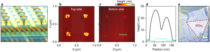
Our sample contains a monolayer of WSe2, synthesized by chemical vapor deposition and encapsulated in hBN. In the top hBN layer, we incorporated a plasmonic gold nanodisk array by dry-etching air-holes into hBN and filling them with gold (details in Methods), with an illustration of the metasurface shown in Fig. 1a. Atomic force micrographs of the top and bottom sides of the hBN layer with the incorporated gold lattice are shown in Figs. 1b, c and linecuts of the height profiles in Fig. 1d, clearly indicating that the bottom side (roughness nm) is significantly smoother than the top side, with the additional advantage that it was not directly exposed to any processing. The hBN-gold layer was then transferred on top of the TMD monolayer, providing a flat and clean interface and immediate proximity to the near-field of the plasmonic SLRs. The robustness of the lattice allows consequent pickup of the TMD monolayer via the hot-pickup technique [11], with an optical micrograph of the heterostructure shown in Fig. 1e.
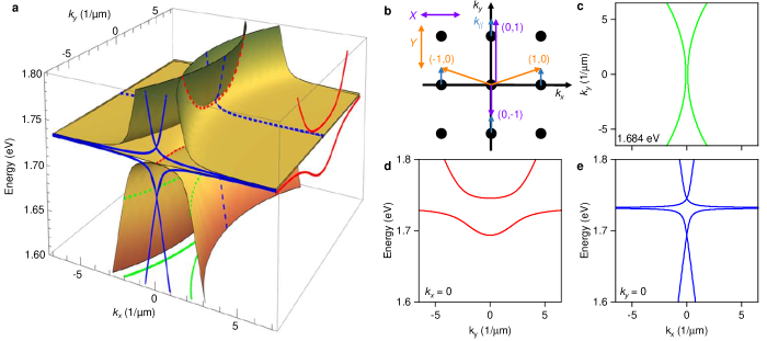
The SLR dispersions are described with a geometric model of the diffractive orders of the lattice [9], illustrated in Fig. 2b for momentum along the axis (see Methods for details). Strong coupling of the bright exciton X to the plasmonic SLRs gives rise to exciton-polaritons with the energy dispersion of the upper (E) and lower (E) polariton branches given as (see Methods for details):
| (1) |
where E (E) and () are the exciton (SLR) energy and half-width at half-maximum linewidth, respectively, and denotes the light-matter coupling strength. A three-dimensional (3D) plot of the upper and lower polariton branches formed by the -polarized () diffractive orders is shown in Fig. 2a, and the corresponding 2D projections in Figs. 2c – e.
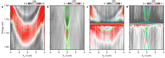
Using momentum-resolved differential reflectance (DR) spectroscopy, we first studied the SLRs on the bare lattice with -polarized broad-band excitation and detection along (), shown in Fig. 3a (Fig. 3b). The SLR dispersions, fitted with Eq. (2) in Methods, are degenerate hyperbolic (Fig. 3a) or non-degenerate linear (Fig. 3b), depending on the combination of excitation and detection axes, and show a linewidth of meV, much narrower than for localized surface plasmons at the same energy [37], corresponding to a Q factor of 32. In the metasurface region, we observe an avoided crossing and the formation of the upper and lower polariton branches (Figs. 3c, d). By fitting Eq. (1), we extracted meV and obtained a Rabi splitting of meV (see Methods for details), much larger than previously reported for polaritons in a TMD monolayer coupled to a dielectric metasurface [25]. Our sample clearly fulfills the common criteria for strong coupling, and [38, 39], with meV.
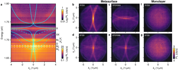
To probe the emission characteristics, we studied the sample in momentum-resolved photoluminescence (PL) spectroscopy (Fig. 4a). The WSe2 monolayer spectrum is known to be rich: in addition to X and its upper and lower polariton branches, we observe two dipolar transitions red-shifted from X by and meV, labeled as XX and D, which are the biexciton [40, 41, 42, 43] and spin-forbidden dark exciton [44, 45], respectively. A series of peaks labeled M1 through M3 also overlap in energy with the lower polariton branches. The assignment of M1 at meV red-shift remains ambiguous, with direct PL emission from momentum-indirect [46, 47, 48] or a phonon sideband of excitons [49] as possible origins. Around M1 is the negative trion doublet X and X with meV exchange splitting [50], visible in our sample due to residual doping. M2 and M3, at and meV red-shift have been assigned to phonon sidebands of momentum-indirect excitons [46, 47].
We chose a narrow energy range around M2 ( eV) because this phonon sideband does not have any oscillator strength, as it arises from exciton-phonon coupling without any direct absorption or emission of photons, and thus cannot couple to the SLRs, and performed polarization-resolved momentum-space imaging (Figs. 4b – g). Under linear excitation and co-polarized detection, we observe a linearly polarized, directional far-field emission profile from the metasurface (Fig. 4b), with part of the emission constrained to small angles (going from ° at up to ° at maximum ). For cross-polarized detection, we observe the same signature but rotated by 90° (Fig. 4c). Under circularly polarized excitation and detection, both sets of linear branches are observed simultaneously (Figs. 4d, e). In contrast, on a bare monolayer, the emission profile is Gaussian (Figs. 4f, g), as expected for excitons with out-of-plane dipolar emission profile [51]. The directional narrow-angle emission of the metasurface is a clear signature of the lower polariton branches (cf. Fig. 2c).
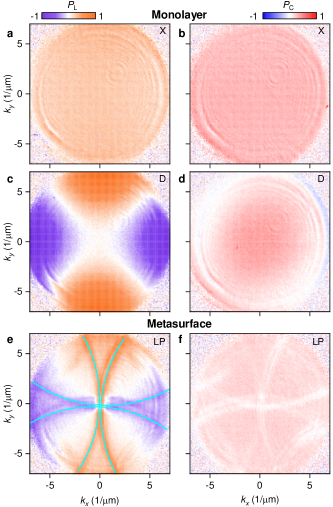
The degrees of linear () and circular () polarization, determined from polarization resolved PL as , where are the co/cross-polarized PL intensities, are shown in Fig. 5. The bright exciton X in monolayer WSe2 (Figs. 5a, b) shows both positive and due to valley-coherence and valley-polarization, respectively [52, 19, 53, 54]. The dark exciton D has an out-of-plane polarized optical dipole with in-plane emission [51], showing zero and finite at small and large and zero at large (Fig. 5c, d). In contrast, the lower polariton shows large up to and near zero along the branches of its dispersions (Figs. 5e, f), effectively imprinting the polarization of the plasmonic lattice onto the WSe2 monolayer via strong coupling.
In conclusion, we have demonstrated strong coupling and a linearly polarized emission profile in a TMD-based metasurface using a novel fabrication method. We integrated a gold plasmonic lattice directly into an hBN layer, preserving dielectric encapsulation of the TMD, while providing immediate proximity to the near-field of the plasmonic SLRs, resulting in enhanced coupling strength and good optical quality, characterized by narrow exciton linewidths. We demonstrated polaritons with a Rabi splitting of meV and a strongly modified emission profile. The far-field emission profile showed narrow-angle, directional, linearly-polarized lower polariton branches. The linear polarization of the square plasmonic lattice is imprinted onto the TMD via strong coupling, effectively quenching its intrinsic circular polarization. The polarization and emission profiles can be tuned by using different lattice geometries. Employing chiral nanostructres instead of disks would enhance the valley polarization of the TMD monolayer with applications in opto-valleytronics [55, 56, 57].
I Methods
I.1 Sample fabrication
High-quality WSe2 monolayers were synthesized by in-house chemical vapor deposition, and hBN flakes were exfoliated from bulk crystals (NIMS). We fabricated gold nanodisk arrays embedded in hBN by employing electron-beam lithography (EBL) and inductively-coupled plasma (ICP) etching. A square array of nm diameter nanodisks was defined via EBL using PMMA 950 K resist with a thickness of around nm and a dose of C/cm2. Air-holes were etched into the hBN via ICP. The plasma was fed by sccm of Ar and sccm of SF6 at a constant chamber pressure of mTorr. Setting the ICP power to W and the RF power to W yielded a controlled etch rate of nm/s. After etching, a gold film matching the thickness of the hBN layer was deposited via electron-beam evaporation. The hardened resist was lifted-off in acetone and isopropanol, and remaining residues were removed in an O2 asher.
A common figure of merit for etched nanostructures is the sidewall verticality, with efforts invested in achieving vertical nanostructures in hBN [58, 59, 60]. Reactive ion etching and electron-beam induced etching were used to create almost vertical sidewalls [59], while a single ICP step achieved etch verticality up to 80° in micron-scale structures with very high etch rates [58]. In this work, we achieved a sidewall angle of around 60° with a good control over the etch time, yielding nm diameter holes, and consequently nanodisks, with flat bottom sides. While the disk shape on the top side is influenced by the sidewall inclination, the bottom side showed a roughness below nm, as highlighted in Figs. 1b – d.
For the design of the gold nanodisk array, we used the finite-difference time-domain method (software Lumerical). The resonance width of SLRs does not depend strongly on the lattice geometry [61]. We designed the structures as gold disks organized on a square lattice with a lattice constant of nm, disk diameters of nm, and a height of nm (matching the hBN thickness). We then selected the thickness of the second hBN layer such that the simulated resonance energy matched the energy of the bright exciton X in monolayer WSe2.
For transfer, we used a dry stamping method with a polydimethylsiloxane (PDMS) droplet on a glass slide as stamp base, which we covered with a thin film of poly-bisphenol A-carbonate (PC, Sigma Aldrich) or polycaprolacton (PCL, Sigma Aldrich). We created the PC (PCL) film by dispersing a solution of polymer dissolved in chloroform (tetrahydrofurane, THF) at a mass percentage of 8 % (15 %). A nm bottom hBN flake was picked up with a PC stamp at °C, released onto a glass substrate at °C, and cleaned in chloroform, acetone, and isopropanol. For the pick-up of the hBN flake with the incorporated gold lattice, a PCL stamp was used. We started the process at 30∘C and heated up to 57∘C to cover the entire flake with the stamp. At this temperature just below its melting point (60∘C), PCL becomes viscous and highly sticky [62]. After cooling back down to 30∘C, we lifted the flake with embedded lattice off the substrate and released it onto a WSe2 monolayer at 75∘C, followed by cleaning in THF, acetone, and isopropanol. Then a PC stamp was used to pick up the stack at °C, followed by release onto the bottom hBN flake at °C. The sample was cleaned in chloroform, acetone, and isopropanol and annealed in ultrahigh vacuum for h at °C to remove trapped air and residues.
I.2 Optical spectroscopy
Cryogenic DR and PL spectroscopy were performed in back-scattering geometry in a closed-cycle cryostat (attocube systems, attoDRY800) with K base temperature. To position the sample with respect to a low temperature apochromatic objective (LT-APO/633-RAMAN/0.81), we used piezo-units (attocube systems, ANPx101, ANPz101, and ANSxy100). Angle-resolved DR and PL spectra were recorded with a lab-built Fourier imaging setup in 4f and telescope configuration employing four achromatic doublet lenses (Edmund Optics, VIS-NIR with focal lengths of , , and mm) and including a dove prism to rotate the Fourier image. The signal was dispersed by a monochromator (Teledyne Princeton Instruments, IsoPlane SCT320), with a 300 grooves/mm grating and detected by a Peltier-cooled (Teledyne Princeton Instruments, PIXIS 1024) charge-coupled device (CCD). Narrow-energy momentum-space images were recorded by turning two tunable filters (Semrock 790 nm VersaChrome Edge tunable Shortpass and Longpass Filters) and by moving the spectrometer grating to zero order and opening the slit. The conversion of camera pixel to wavevector in 1/m was obtained via the size of the illuminated area on the CCD and using the relation with the maximum angle given by the numerical aperture of the objective, and . For both DR and PL measurements, we used a pulsed supercontinuum laser (NKT Photonics, SuperK with Varia). DR was defined as , where was the reflactance from the sample and was the reference reflectance from a region containing only hBN. PL was excited near the WSe2 2s resonance (first higher excited state of X in the exciton Rydberg series [63]) at nm and W.
I.3 SLR and polariton dispersions
The SLR dispersions are described by a geometric model of the diffractive orders of the lattice [9], illustrated in Fig. 2b. The -vector of the SLRs is given by and their energy by:
| (2) |
with lattice constant , diffractive orders , and effective refractive index . At , . By fitting Eq. (2) to the dispersions measured at different positions on the uncoupled lattice over an area of m2, we determined an average , corresponding to eV at . We determined the SLR half-width at half-maximum linewidth as meV by fitting a Gaussian at in phase-corrected (with Kramers-Kronig relation) DR. Under linearly polarized excitation, light couples either to the or diffractive orders, which show degenerate hyperbolic or non-degenerate linear energy dispersions depending on the combination of linear polarization and -space detection axes.
In the metasurface region, we observe exciton-polariton formation. We fit a coupled oscillator model [64, 27] with the Hamiltonian:
| (3) |
Diagonalization yields the well-known energy relation for the upper and lower polariton branches given by Eq. (1) in the main text. By fitting Eq. (1) to the dispersions measured at different positions over an area of m2 of the metasurface with meV (determined by Lorentzian fitting of the phase-corrected DR on a monolayer region) and meV, we extracted meV, , and eV.
The Rabi splitting is defined as [39]:
| (4) |
and is meV. The linewidth of the lower polariton branch is given by [65]:
| (5) |
where and are the Hopfield coefficients [39]:
| (6) | ||||
| (7) |
and shown as dashed cyan lines in Figs. 3c and 4a for the hyperbolic polariton dispersion.
Author Information
Corresponding authors:
F. T.-V. (f.tabataba@lmu.de) and A. H. (alexander.hoegele@lmu.de).
Author Contributions:
F. T.-V. and L. K. contributed equally to this work.
Notes:
The authors declare no competing financial interest.
Acknowledgements: This research was funded by the European Research Council (ERC) under the Grant Agreement No. 772195 and the Deutsche Forschungsgemeinschaft (DFG, German Research Foundation) within Germany’s Excellence Strategy under grant No. EXC-2111-390814868. F. T.-V. acknowledges funding from the Munich Center for Quantum Science and Technology (MCQST) and the European Union’s Framework Programme for Research and Innovation Horizon Europe under the Marie Skłodowska-Curie Actions grant agreement No. 101058981. K. W. and T. T. acknowledge support from the JSPS KAKENHI (Grant Numbers 20H00354 and 23H02052) and World Premier International Research Center Initiative (WPI), MEXT, Japan.
References
- Yu and Capasso [2014] N. Yu and F. Capasso, Flat optics with designer metasurfaces, Nat. Mater. 13, 139 (2014).
- Meinzer et al. [2014] N. Meinzer, W. L. Barnes, and I. R. Hooper, Plasmonic meta-atoms and metasurfaces, Nat. Photonics 8, 889 (2014).
- Chen et al. [2016] H.-T. Chen, A. J. Taylor, and N. Yu, A review of metasurfaces: physics and applications, Rep. Prog. Phys. 79, 076401 (2016).
- Yu et al. [2011] N. Yu, P. Genevet, M. A. Kats, F. Aieta, J.-P. Tetienne, F. Capasso, and Z. Gaburro, Light propagation with phase discontinuities: generalized laws of reflection and refraction, Science 334, 333 (2011).
- Huang et al. [2013] L. Huang, X. Chen, H. Mühlenbernd, H. Zhang, S. Chen, B. Bai, Q. Tan, G. Jin, K.-W. Cheah, C.-W. Qiu, J. Li, T. Zentgraf, and S. Zhang, Three-dimensional optical holography using a plasmonic metasurface, Nat. Commun. 4, 2808 (2013).
- Aieta et al. [2012] F. Aieta, P. Genevet, M. A. Kats, N. Yu, R. Blanchard, Z. Gaburro, and F. Capasso, Aberration-free ultrathin flat lenses and axicons at telecom wavelengths based on plasmonic metasurfaces, Nano Lett. 12, 4932 (2012).
- Deng et al. [2020] S. Deng, R. Li, J.-E. Park, J. Guan, P. Choo, J. Hu, P. J. Smeets, and T. W. Odom, Ultranarrow plasmon resonances from annealed nanoparticle lattices, Proc. Natl. Acad. Sci. U.S.A. 117, 23380 (2020).
- Cherqui et al. [2019] C. Cherqui, M. R. Bourgeois, D. Wang, and G. C. Schatz, Plasmonic surface lattice resonances: Theory and computation, Acc. Chem. Res. 52, 2548 (2019).
- Guo et al. [2017] R. Guo, T. K. Hakala, and P. Törmä, Geometry dependence of surface lattice resonances in plasmonic nanoparticle arrays, Phys. Rev. B 95, 155423 (2017).
- Meng et al. [2023] Y. Meng, H. Zhong, Z. Xu, T. He, J. S. Kim, S. Han, S. Kim, S. Park, Y. Shen, M. Gong, Q. Xiao, and S.-H. Bae, Functionalizing nanophotonic structures with 2D van der Waals materials, Nanoscale Horiz. 8, 1345 (2023).
- Pizzocchero et al. [2016] F. Pizzocchero, L. Gammelgaard, B. S. Jessen, J. M. Caridad, L. Wang, J. Hone, P. Bøggild, and T. J. Booth, The hot pick-up technique for batch assembly of van der Waals heterostructures, Nat. Commun. 7, 11894 (2016).
- Splendiani et al. [2010] A. Splendiani, L. Sun, Y. Zhang, T. Li, J. Kim, C.-Y. Chim, G. Galli, and F. Wang, Emerging photoluminescence in monolayer MoS2, Nano Lett. 10, 1271 (2010).
- Mak et al. [2010] K. F. Mak, C. Lee, J. Hone, J. Shan, and T. F. Heinz, Atomically thin MoS2: a new direct-gap semiconductor, Phys. Rev. Lett. 105, 136805 (2010).
- He et al. [2014] K. He, N. Kumar, L. Zhao, Z. Wang, K. F. Mak, H. Zhao, and J. Shan, Tightly bound excitons in monolayer WSe2, Phys. Rev. Lett. 113, 026803 (2014).
- Chernikov et al. [2014] A. Chernikov, T. C. Berkelbach, H. M. Hill, A. Rigosi, Y. Li, B. Aslan, D. R. Reichman, M. S. Hybertsen, and T. F. Heinz, Exciton binding energy and nonhydrogenic Rydberg series in monolayer WS2, Phys. Rev. Lett. 113, 076802 (2014).
- Zhang et al. [2014] C. Zhang, H. Wang, W. Chan, C. Manolatou, and F. Rana, Absorption of light by excitons and trions in monolayers of metal dichalcogenide MoS2: Experiments and theory, Phys. Rev. B 89, 205436 (2014).
- Li et al. [2014] Y. Li, A. Chernikov, X. Zhang, A. Rigosi, H. M. Hill, A. M. Van Der Zande, D. A. Chenet, E.-M. Shih, J. Hone, and T. F. Heinz, Measurement of the optical dielectric function of monolayer transition-metal dichalcogenides: MoS2, MoSe2, WS2, and WSe2, Phys. Rev. B 90, 205422 (2014).
- Xiao et al. [2012] D. Xiao, G.-B. Liu, W. Feng, X. Xu, and W. Yao, Coupled spin and valley physics in monolayers of MoS2 and other group-VI dichalcogenides, Phys. Rev. Lett. 108, 196802 (2012).
- Mak et al. [2012] K. F. Mak, K. He, J. Shan, and T. F. Heinz, Control of valley polarization in monolayer MoS2 by optical helicity, Nat. Nanotechnol. 7, 494 (2012).
- Wang et al. [2018] G. Wang, A. Chernikov, M. M. Glazov, T. F. Heinz, X. Marie, T. Amand, and B. Urbaszek, Colloquium: Excitons in atomically thin transition metal dichalcogenides, Rev. Mod. Phys. 90, 021001 (2018).
- Van de Groep et al. [2020] J. Van de Groep, J.-H. Song, U. Celano, Q. Li, P. G. Kik, and M. L. Brongersma, Exciton resonance tuning of an atomically thin lens, Nat. Photonics 14, 426 (2020).
- Sun et al. [2019] L. Sun, C.-Y. Wang, A. Krasnok, J. Choi, J. Shi, J. S. Gomez-Diaz, A. Zepeda, S. Gwo, C.-K. Shih, A. Alù, and X. Li, Separation of valley excitons in a MoS2 monolayer using a subwavelength asymmetric groove array, Nat. Photonics 13, 180 (2019).
- Dufferwiel et al. [2015] S. Dufferwiel, S. Schwarz, F. Withers, A. Trichet, F. Li, M. Sich, O. Del Pozo-Zamudio, C. Clark, A. Nalitov, D. Solnyshkov, G. Malpuech, K. S. Novoselov, J. M. Smith, M. S. Skolnick, D. N. Krizhanovskii, and A. I. Tartakovskii, Exciton–polaritons in van der Waals heterostructures embedded in tunable microcavities, Nat. Commun. 6, 8579 (2015).
- Liu et al. [2015] X. Liu, T. Galfsky, Z. Sun, F. Xia, E.-c. Lin, Y.-H. Lee, S. Kéna-Cohen, and V. M. Menon, Strong light–matter coupling in two-dimensional atomic crystals, Nat. Photonics 9, 30 (2015).
- Chen et al. [2020] Y. Chen, S. Miao, T. Wang, D. Zhong, A. Saxena, C. Chow, J. Whitehead, D. Gerace, X. Xu, S.-F. Shi, and A. Majumdar, Metasurface integrated monolayer exciton polariton, Nano Lett. 20, 5292 (2020).
- Liu et al. [2016] W. Liu, B. Lee, C. H. Naylor, H.-S. Ee, J. Park, A. C. Johnson, and R. Agarwal, Strong exciton–plasmon coupling in MoS2 coupled with plasmonic lattice, Nano Lett. 16, 1262 (2016).
- Wang et al. [2019] S. Wang, Q. Le-Van, F. Vaianella, B. Maes, S. Eizagirre Barker, R. H. Godiksen, A. G. Curto, and J. Gomez Rivas, Limits to strong coupling of excitons in multilayer WS2 with collective plasmonic resonances, ACS Photonics 6, 286 (2019).
- Liu et al. [2019] W. Liu, Y. Wang, B. Zheng, M. Hwang, Z. Ji, G. Liu, Z. Li, V. J. Sorger, A. Pan, and R. Agarwal, Observation and active control of a collective polariton mode and polaritonic band gap in few-layer WS2 strongly coupled with plasmonic lattices, Nano Lett. 20, 790 (2019).
- Khatibi et al. [2018] Z. Khatibi, M. Feierabend, M. Selig, S. Brem, C. Linderälv, P. Erhart, and E. Malic, Impact of strain on the excitonic linewidth in transition metal dichalcogenides, 2D Mater. 6, 015015 (2018).
- Raja et al. [2019] A. Raja, L. Waldecker, J. Zipfel, Y. Cho, S. Brem, J. D. Ziegler, M. Kulig, T. Taniguchi, K. Watanabe, E. Malic, T. F. Heinz, T. C. Berkelbach, and A. Chernikov, Dielectric disorder in two-dimensional materials, Nat. Nanotechnol. 14, 832 (2019).
- Cadiz et al. [2017] F. Cadiz, E. Courtade, C. Robert, G. Wang, Y. Shen, H. Cai, T. Taniguchi, K. Watanabe, H. Carrere, D. Lagarde, M. Manca, T. Amand, P. Renucci, S. Tongay, X. Marie, and B. Urbaszek, Excitonic linewidth approaching the homogeneous limit in MoS2-based van der Waals heterostructures, Phys. Rev. X 7, 021026 (2017).
- Wang et al. [2016a] S. Wang, S. Li, T. Chervy, A. Shalabney, S. Azzini, E. Orgiu, J. A. Hutchison, C. Genet, P. Samorì, and T. W. Ebbesen, Coherent coupling of WS2 monolayers with metallic photonic nanostructures at room temperature, Nano Lett. 16, 4368 (2016a).
- Sun et al. [2021] J. Sun, Y. Li, H. Hu, W. Chen, D. Zheng, S. Zhang, and H. Xu, Strong plasmon–exciton coupling in transition metal dichalcogenides and plasmonic nanostructures, Nanoscale 13, 4408 (2021).
- Guo et al. [2023] C. Guo, J. Yu, and S. Deng, Hybrid metasurfaces of plasmonic lattices and 2D materials, Adv. Funct. Mater. 33, 2302265 (2023).
- Klein et al. [2019] M. Klein, B. H. Badada, R. Binder, A. Alfrey, M. McKie, M. R. Koehler, D. G. Mandrus, T. Taniguchi, K. Watanabe, B. J. LeRoy, and J. R. Schaibley, 2D semiconductor nonlinear plasmonic modulators, Nat. Commun. 10, 3264 (2019).
- Dibos et al. [2019] A. M. Dibos, Y. Zhou, L. A. Jauregui, G. Scuri, D. S. Wild, A. A. High, T. Taniguchi, K. Watanabe, M. D. Lukin, P. Kim, and H. Park, Electrically tunable exciton–plasmon coupling in a WSe2 monolayer embedded in a plasmonic crystal cavity, Nano Lett. 19, 3543 (2019).
- Vadia et al. [2023] S. Vadia, J. Scherzer, K. Watanabe, T. Taniguchi, and A. Högele, Magneto-optical chirality in a coherently coupled exciton–plasmon system, Nano Lett. 23, 614 (2023).
- Baranov et al. [2018] D. G. Baranov, M. Wersall, J. Cuadra, T. J. Antosiewicz, and T. Shegai, Novel nanostructures and materials for strong light–matter interactions, ACS Photonics 5, 24 (2018).
- Schneider et al. [2018] C. Schneider, M. M. Glazov, T. Korn, S. Höfling, and B. Urbaszek, Two-dimensional semiconductors in the regime of strong light-matter coupling, Nat. Commun. 9, 2695 (2018).
- You et al. [2015] Y. You, X.-X. Zhang, T. C. Berkelbach, M. S. Hybertsen, D. R. Reichman, and T. F. Heinz, Observation of biexcitons in monolayer WSe2, Nat. Phys. 11, 477 (2015).
- Barbone et al. [2018] M. Barbone, A. R.-P. Montblanch, D. M. Kara, C. Palacios-Berraquero, A. R. Cadore, D. De Fazio, B. Pingault, E. Mostaani, H. Li, B. Chen, K. Watanabe, T. Taniguchi, S. Tongay, G. W. amd Andrea C. Ferrari, and M. Atatüre, Charge-tuneable biexciton complexes in monolayer WSe2, Nat. Commun. 9, 3721 (2018).
- Li et al. [2018] Z. Li, T. Wang, Z. Lu, C. Jin, Y. Chen, Y. Meng, Z. Lian, T. Taniguchi, K. Watanabe, S. Zhang, D. Smirnov, and S.-F. Shi, Revealing the biexciton and trion-exciton complexes in BN encapsulated WSe2, Nat. Commun. 9, 3719 (2018).
- Steinhoff et al. [2018] A. Steinhoff, M. Florian, A. Singh, K. Tran, M. Kolarczik, S. Helmrich, A. W. Achtstein, U. Woggon, N. Owschimikow, F. Jahnke, and X. Li, Biexciton fine structure in monolayer transition metal dichalcogenides, Nat. Phys. 14, 1199 (2018).
- Zhang et al. [2015] X.-X. Zhang, Y. You, S. Y. F. Zhao, and T. F. Heinz, Experimental evidence for dark excitons in monolayer WSe2, Phys. Rev. Lett. 115, 257403 (2015).
- Robert et al. [2017] C. Robert, T. Amand, F. Cadiz, D. Lagarde, E. Courtade, M. Manca, T. Taniguchi, K. Watanabe, B. Urbaszek, and X. Marie, Fine structure and lifetime of dark excitons in transition metal dichalcogenide monolayers, Phys. Rev. B 96, 155423 (2017).
- He et al. [2020] M. He, P. Rivera, D. Van Tuan, N. P. Wilson, M. Yang, T. Taniguchi, K. Watanabe, J. Yan, D. G. Mandrus, H. Yu, H. Dery, W. Yao, and X. Xu, Valley phonons and exciton complexes in a monolayer semiconductor, Nat. Commun. 11, 618 (2020).
- Liu et al. [2020] E. Liu, J. van Baren, C.-T. Liang, T. Taniguchi, K. Watanabe, N. M. Gabor, Y.-C. Chang, and C. H. Lui, Multipath optical recombination of intervalley dark excitons and trions in monolayer WSe2, Phys. Rev. Lett. 124, 196802 (2020).
- Yang et al. [2022] M. Yang, L. Ren, C. Robert, D. Van Tuan, L. Lombez, B. Urbaszek, X. Marie, and H. Dery, Relaxation and darkening of excitonic complexes in electrostatically doped monolayer WSe2: Roles of exciton-electron and trion-electron interactions, Phys. Rev. B 105, 085302 (2022).
- Förste et al. [2020] J. Förste, N. V. Tepliakov, S. Y. Kruchinin, J. Lindlau, V. Funk, M. Förg, K. Watanabe, T. Taniguchi, A. S. Baimuratov, and A. Högele, Exciton g-factors in monolayer and bilayer WSe2 from experiment and theory, Nat. Commun. 11, 4539 (2020).
- Courtade et al. [2017] E. Courtade, M. Semina, M. Manca, M. Glazov, C. Robert, F. Cadiz, G. Wang, T. Taniguchi, K. Watanabe, M. Pierre, W. Escoffier, E. L. Ivchenko, P. Renucci, X. Marie, T. Amand, and B. Urbaszek, Charged excitons in monolayer WSe2: Experiment and theory, Phys. Rev. B 96, 085302 (2017).
- Wang et al. [2017] G. Wang, C. Robert, M. M. Glazov, F. Cadiz, E. Courtade, T. Amand, D. Lagarde, T. Taniguchi, K. Watanabe, B. Urbaszek, and X. Marie, In-plane propagation of light in transition metal dichalcogenide monolayers: optical selection rules, Phys. Rev. Lett. 119, 047401 (2017).
- Zeng et al. [2012] H. Zeng, J. Dai, W. Yao, D. Xiao, and X. Cui, Valley polarization in MoS2 monolayers by optical pumping, Nat. Nanotechnol. 7, 490 (2012).
- Jones et al. [2013] A. M. Jones, H. Yu, N. J. Ghimire, S. Wu, G. Aivazian, J. S. Ross, B. Zhao, J. Yan, D. G. Mandrus, D. Xiao, W. Yao, and X. Xu, Optical generation of excitonic valley coherence in monolayer WSe2, Nat. Nanotechnol. 8, 634 (2013).
- Wang et al. [2016b] G. Wang, X. Marie, B. Liu, T. Amand, C. Robert, F. Cadiz, P. Renucci, and B. Urbaszek, Control of exciton valley coherence in transition metal dichalcogenide monolayers, Phys. Rev. Lett. 117, 187401 (2016b).
- Gong et al. [2018] S.-H. Gong, F. Alpeggiani, B. Sciacca, E. C. Garnett, and L. Kuipers, Nanoscale chiral valley-photon interface through optical spin-orbit coupling, Science 359, 443 (2018).
- Hu et al. [2019] G. Hu, X. Hong, K. Wang, J. Wu, H.-X. Xu, W. Zhao, W. Liu, S. Zhang, F. Garcia-Vidal, B. Wang, P. Lu, and C.-W. Qiu, Coherent steering of nonlinear chiral valley photons with a synthetic Au–WS2 metasurface, Nat. Photonics 13, 467 (2019).
- Guddala et al. [2019] S. Guddala, R. Bushati, M. Li, A. Khanikaev, and V. Menon, Valley selective optical control of excitons in 2D semiconductors using a chiral metasurface, Opt. Mater. Express 9, 536 (2019).
- Grenadier et al. [2013] S. Grenadier, J. Li, J. Lin, and H. Jiang, Dry etching techniques for active devices based on hexagonal boron nitride epilayers, J. Vac. Sci. Technol. A 31 (2013).
- Fröch et al. [2019] J. E. Fröch, Y. Hwang, S. Kim, I. Aharonovich, and M. Toth, Photonic nanostructures from hexagonal boron nitride, Adv. Opt. Mater. 7, 1801344 (2019).
- Kühner et al. [2023] L. Kühner, L. Sortino, B. Tilmann, T. Weber, K. Watanabe, T. Taniguchi, S. A. Maier, and A. Tittl, High-Q nanophotonics over the full visible spectrum enabled by hexagonal boron nitride metasurfaces, Adv. Mater. 35, 2209688 (2023).
- Humphrey and Barnes [2014] A. D. Humphrey and W. L. Barnes, Plasmonic surface lattice resonances on arrays of different lattice symmetry, Phys. Rev. B 90, 075404 (2014).
- Son et al. [2020] S. Son, Y. J. Shin, K. Zhang, J. Shin, S. Lee, H. Idzuchi, M. J. Coak, H. Kim, J. Kim, J. H. Kim, M. Kim, D. Kim, P. Kim, and J.-G. Park, Strongly adhesive dry transfer technique for van der Waals heterostructure, 2D Mater. 7, 041005 (2020).
- Stier et al. [2018] A. V. Stier, N. P. Wilson, K. A. Velizhanin, J. Kono, X. Xu, and S. A. Crooker, Magnetooptics of exciton Rydberg states in a monolayer semiconductor, Phys. Rev. Lett. 120, 057405 (2018).
- Shi et al. [2014] L. Shi, T. Hakala, H. Rekola, J.-P. Martikainen, R. Moerland, and P. Törmä, Spatial coherence properties of organic molecules coupled to plasmonic surface lattice resonances in the weak and strong coupling regimes, Phys. Rev. Lett. 112, 153002 (2014).
- Deng et al. [2010] H. Deng, H. Haug, and Y. Yamamoto, Exciton-polariton Bose-Einstein condensation, Rev. Mod. Phys. 82, 1489 (2010).