Present address: ]Department of Applied Physics and Applied Mathematics,
Columbia University, New York, NY, USA
Striped Electronic Phases in an Incommensurately
Modulated van der Waals Superlattice
The electronic properties of crystalline materials can be manipulated by superimposing spatially periodic electric, magnetic, or structural modulations. Systems with long-wavelength modulations incommensurate with the atomic lattice are of particular interest [1], exemplified by recent advances with moiré patterned two-dimensional (2D) van der Waals (vdW) heterostructures [2, 3]. Bulk vdW superlattices [4, 5, 6, 7, 8] hosting 2D interfaces between minimally disordered layers represent scalable bulk analogs of artificial vdW heterostructures and present a complementary venue to explore incommensurately modulated 2D states. Here we report the bulk vdW superlattice \ceSrTa2S5 realizing an incommensurate one-dimensional (1D) structural modulation of 2D transition metal dichalcogenide (TMD) -\ceTaS2 layers. High-quality electronic transport in the -\ceTaS2 layers, evidenced by quantum oscillations, is made anisotropic by the modulation and exhibits commensurability oscillations [9] paralleling lithographically modulated 2D systems [10, 11, 12]. We also find unconventional, clean-limit superconductivity (SC) in \ceSrTa2S5 with a pronounced suppression of interlayer coherence relative to intralayer coherence. Such a hierarchy of energy scales can arise from pair-density wave (PDW) SC with mismatched spatial arrangement in adjacent superconducting layers [13, 14, 15]. Examining the in-plane magnetic field () dependence of interlayer critical current density , we observe anisotropy with respect to orientation: is maximized (minimized) when is perpendicular (parallel) to the stripes, consistent with 1D PDW SC [16, 17, 18]. Electron diffraction shows the structural stripe modulation is phase-shifted between adjacent -\ceTaS2 layers, suggesting mismatched 1D PDW is seeded by the striped structure. Hosting a high-mobility Fermi liquid in a coherently modulated structure, \ceSrTa2S5 is a promising venue for unusual phenomena anticipated in clean, striped metals and superconductors [19, 20, 21]. More broadly, \ceSrTa2S5 establishes bulk vdW superlattices as versatile platforms to address long-standing predictions surrounding modulated electronic phases in the form of macroscopic crystals [22, 23].
Incommensuration in crystals arises from the coexistence of two or more mutually incompatible periodicities [24]. Incommensuration can appear in forms spanning magnetic modulations in rare earth metals [25, 26], arrangement of ions and molecules in graphite intercalation compounds [27], and incommensurate charge density waves (CDWs) in metallic systems [28]. Another prominent class is structurally incommensurate materials where incommensuration appears as a spatial modulation of the crystal lattice. These materials, with mismatched periodicities of the lattice and incommensurate modulation, are beyond the usual description of crystals and motivated the formulation of superspace group methods to describe their structures [29]. If the incommensurate modulation is weak and has a longer wavelength compared to the lattice periodicity, it can act as a perturbation to the underlying crystal [30], presenting a means to manipulate their electronic behavior and design phases beyond those found in conventional crystals.
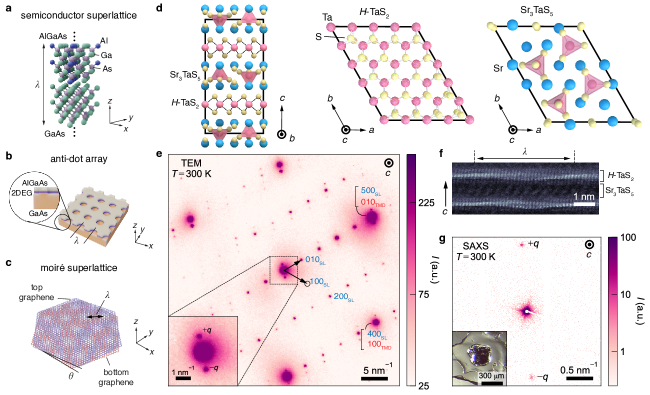
Semiconductor superlattices [31] are early examples of engineered incommensuration where one-dimensional (1D) periodic modulations along the growth direction (Fig. 1a) are created by varying the chemical composition, for example, periodic aluminum (Al) doping into gallium arsenide (GaAs). Incommensuration is achieved therein by engineering the modulation wavelength such that is irrational ( is the crystal lattice spacing). Lithographically patterned semiconductor heterostructures are another example (Fig. 1b) with incommensurate modulations superimposed on high-quality 2D electron gases (2DEGs). More recently, moiré patterns at lattice mismatched or rotationally faulted vdW heterointerfaces (Fig. 1c) have emerged as hosts for incommensurately modulated phases. Together, materials with engineered incommensuration have realized various intriguing electronic phenomena: semiconductor superlattices [30, 31, 32] feature electronic mini-bands with non-linear electronic and optical properties, patterned 2DEGs exhibit novel commensurabilty resonances [10, 11], and moiré patterned vdW heterostructures host an array of emergent correlated and topological phases [3, 33, 34]. A notable aspect of these existing platforms is their exceptionally low atomic-scale disorder, supporting high-mobility transport and fragile electronic ground states. Thermodynamically stable, incommensurately modulated bulk materials with comparable quality are desirable as readily accessible, complementary platforms to study modulated electronic states. Apart from fragile organic conductors [35], modulated bulk materials exhibit relatively low electronic mobilities (Sec. SIII).
Here we report a bulk vdW superlattice [4, 5, 7, 8] which naturally forms a macroscopically uniform incommensurate structural modulation with pronounced effects on its electronic behavior. The material \ceSrTa2S5 is composed of -\ceTaS2 TMD and \ceSr3TaS5 spacer layers stacked in an alternating fashion (see Fig. 1d, left). In the average structure, the latter has a 2-fold symmetric in-plane structure (monoclinic point group ) which forms a commensurate superstructure with 3-fold symmetric -\ceTaS2 (hexagonal point group ) (Fig. 1d, right and Sec. SIa). Figure 1e shows an electron diffraction pattern of the -plane structure where these features can be identified. We find dominant reflections from -\ceTaS2 (Fig. 1e, red) and superstructure reflections from monoclinic \ceSr3TaS5 (Fig. 1e, blue). We also observe satellite reflections at (Fig. 1e, inset) from a long-wavelength 1D modulation. Using we estimate nm. The -vector has an irrational relationship with the reciprocal lattice of the average structure, evidencing incommensuration (section SIb). High-resolution synchrotron powder x-ray diffraction (PXRD) shows the TMD layers are weakly strained towards commensuration with the spacers to form the superstructure (section SIb). This parallels misfit superlattices [36, 37] and in-plane TMD heterointerfaces [38] where translation symmetry mismatch gives rise to incommensurate structural modulations.
The 1D stripes are apparent in cross-section (Fig. 1f) and -plane (see Fig. S3a) transmission electron microscopy (TEM) images. We observe an out-of-plane distortion of the -\ceTaS2 layers with peak-to-valley amplitude Å and lateral periodicity of several nanometers, consistent with -plane electron diffraction. Cross-section electron diffraction indicates this structural modulation is phase-shifted between adjacent layers (Sec. SIb). Small-angle x-ray scattering (SAXS) at temperature K from the -plane of bulk crystals (Fig. 1g, sample in inset) shows the same pattern of satellite reflections with nm (Methods). Given the x-ray beam spot encompasses an area comparable to the measured crystals, the single pair of sharp reflections demonstrate the incommensurate structural modulation is macroscopically coherent. We hypothesize this large scale coherence is rooted in the low symmetry of the average structure and the 1D nature of the modulation which restricts the allowed modulation directions (section SIb).
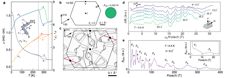
Turning to the electronic properties of \ceSrTa2S5, we examined the dependence of in-plane resistivity perpendicular () and parallel () to using a focused ion beam (FIB) patterned “L-bar” device (Fig. 2a, inset). Similar to the parent TMD 2-\ceTaS2, this system is a metal. Both (Fig. 2a, orange and red) and (Fig. 2a, blue and green) show prominent thermal hysteresis in the range signaling a first-order phase transition. While synchrotron PXRD, SAXS, and electron diffraction do not evidence a structural transition, we find similar thermal hysteresis in torque magnetometry which points to an electronic origin (section SII). Additionally, first-principles calculations (Fig. 2c) reveal Fermi surface (FS) segments centered at B which are well-nested by the modulation -vector (Fig. 2c, red). Together, these point to a first-order lock-in CDW transition as the source of the thermal hysteresis (section SII). At lower the in-plane transport anisotropy (Fig. 2a, gray and purple) increases and reaches at K. Comparable is found in the high-field nematic phase of 2DEGs [39], some stripe-phase cuprates [40], and misfit superlattices [41], suggesting the stripe modulation acts like a perturbation; the in-plane anisotropy is markedly less than that of TMDs such as -\ceWTe2 with quasi-1D intralayer structures [42, 43].
We also observe quantum oscillations in \ceSrTa2S5 that allow us to map its fermiology. Figure 2d shows de Haas-van Alphen (dHvA) oscillations in torque magnetization (section SIII) at K versus the magnetic field component perpendicular to the -plane, ; is the total field and is measured from the -axis (Fig. 2d, inset). Alignment of across various fixed indicates the FSs are cylindrical and aligned along due to weak interlayer coupling. The complex oscillatory behavior of is due to interference amongst numerous oscillation frequencies and corresponding FSs. We extract the individual frequency components from the Fast Fourier Transform (FFT) of . The FFT spectrum for and K is shown in Fig. 2e, exhibiting numerous components spanning T to T (see Sec. SIII), reflecting the complex electronic structure of \ceSrTa2S5 (Fig. 2c). We also find weaker contributions (Fig. 2e, starred) which we ascribe to magnetic breakdown between closely spaced Fermi surfaces (Sec. SIII [44]), further consistent with the complex electronic structure (Fig. 2c).
Using Onsager’s relation (Methods) [45] we find the largest FS of \ceSrTa2S5 encloses an area Å-2 (Fig. 2b) in the Brillouin zone (BZ), smaller than anticipated for -\ceTaS2 (section SIII). This is consistent with zone-folding of the -\ceTaS2 FSs into a nearly smaller Brillouin zone (BZ) of \ceSrTa2S5 due to the superlattice periodicity imposed by the spacer. More broadly, the appearance of quantum oscillations in this incommensurately modulated material is remarkable. From their onset field T (Fig. 2d, black triangle) we estimate a quantum mobility 3,000 cm2/Vs, markedly larger than mobilities seen in 2-\ceTaS2 ( cm2/Vs [46]) and -\ceTaS2 containing misfit-layer compounds ( cm2/Vs [47], Sec SIII). Beyond presenting a bulk platform for exploring phase-coherent electrons in incommensurate potentials [48], the high quality of \ceSrTa2S5 may support exotic but fragile modulated states. Notably, this mobility enhancement parallels that found in the related -\ceNbS2 containing superlattice \ceBa6Nb11S28 relative to 2-\ceNbS2 [5], which suggests this growing family of superlattices generically hosts clean TMD layers.
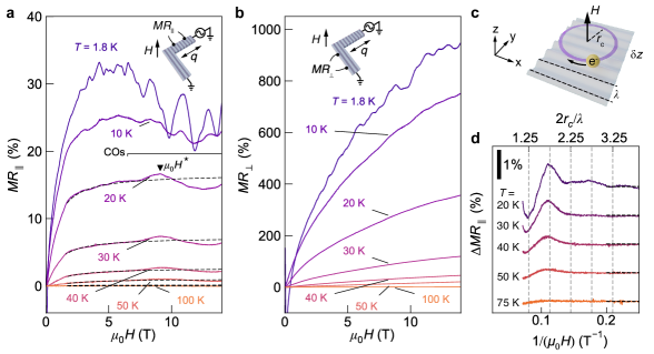
The stripe modulation in \ceSrTa2S5 leads to additional transport features characteristic of modulated 2DEGs. Figures 3a and 3b show magnetoresistance of the L-bar device measured parallel and perpendicular to , and , respectively (Methods). Together with Shubnikov-de Haas (SdH) oscillations paralleling dHvA oscillations in , we find a low frequency T oscillation in that is absent in (section SIV). Further, this oscillation persists to K unlike dHvA oscillations which are suppressed by K (Fig. S5). The absence of these oscillations in indicates of the stripes is relevant to their observation. The overall phenomenology parallels commensurability oscillations (COs) in stripe-patterned 2DEGs due to matching of the cyclotron diameter and modulation (see Fig. 3c) with frequency where is the Fermi wavevector [9, 10]. Using the observed and nm from SAXS we find Å-1, in nominal agreement with Å-1 of the smallest pocket observed in dHvA oscillations (see Sec. SIII). Moreover, these oscillations exhibit the characteristic period phase shift anticipated for commensurability oscillations (Fig. 3d) [49, 50] and distinct from conventional quantum oscillations [45].
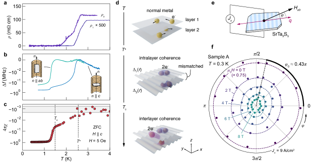
At low superconductivity (SC) emerges from the stripe-modulated metallic state. Comparing the dependence of intralayer (perpendicular to ) and interlayer resistivity, and respectively, we find reaches zero at lower relative to (Fig. 4a), suggesting suppressed interlayer coupling in the superconducting state. We also performed tunnel diode oscillator (TDO) measurements in this low regime, wherein the oscillator frequency reflects changes in screening supercurrents [51, 52] (Methods). The variation of below = 2.5 K, for crystals oriented with their -axis or -plane parallel to the coil axis , sensing the intralayer or interlayer supercurrent response, respectively, exhibit a similar hierarchy of scales (Fig. 4b). For the same sample, we observe that intralayer screening onsets near 2.3 K (Fig. 4b, blue) whereas interlayer screening onsets near 1.4 K (Fig. 4b, green). Similar separation of scales is observed in zero-field cooled (ZFC) magnetic susceptibility for . Below K where crosses ( and denote the mean and standard deviation, respectively), we observe weak diamagnetism consistent with the appearance of intralayer supercurrents (Fig. 4c). This is followed by a Meissner transition at K with a shielding fraction near unity, characteristic of bulk superconductivity (Sec. SVa).
Together these observations establish that intralayer superconducting coherence appears at followed by interlayer coherence at (i.e. superconducting coupling between the layers is frustrated). This sequence of transitions parallels the phenomenology of striped cuprate superconductors such as La1.875Ba0.125CuO4 [13, 15]. In these cuprates, interlayer coherence is thought to be suppressed by pair-density wave (PDW) SC with spatially modulated superconducting order parameter that is mismatched between adjacent \ceCuO2 layers [14, 53]. Recent scanning tunneling microscopy (STM) experiments [54, 55, 56] indicate PDW order is a generic feature of SC emerging from modulated metals, raising \ceSrTa2S5 as a host for 1D PDW SC with . A natural hypothesis is that the inequivalence of the structural modulation in adjacent layers (Sec. SIb) seeds similarly inequivalent . Therefrom, numerous configurations of 1D PDW order mismatched between neighboring layers can suppress interlayer coherence (Sec. SVb) and potentially lead to the observed separation of energy scales (Fig. 4d).
To test this hypothesis, we study the interlayer critical current density versus in-plane magnetic field strength and orientation relative to (Fig. 4e). For finite oriented along , suppression of by mismatched PDW order is partially compensated by the Lorentz boost of Cooper pairs from , which is a global phase-sensitive consequence of PDW SC [16, 17] (Sec. SVc). Correspondingly, takes a characteristic, anisotropic form with enhanced relative to (Sec. SVc) [17, 16, 18]. Figure 4f shows at K for various fixed ; with increasing field, a pronounced 2-fold anisotropy develops. Quantitatively, least-squares fits (Fig. 4f, dashed lines) to (the second term captures partial restoration of by ) reveals . Similar behavior is also observed in a second sample (Sec. SVc). The observed is consistent with anticipated for 1D PDW SC seeded by the structural stripe modulation.
SrTa2S5 is in the clean-limit of superconductivity (Sec. SVa), raising it as a host for various unconventional phases anticipated in clean PDW superconductors [20, 57]. Further, the homogeneity of the incommensurate modulation suggests the PDW is macroscopically uniform which is advantageous for further examination. Also, unlike the cuprates, PDW SC in \ceSrTa2S5 emerges from a high-mobility, stripe-modulated Fermi liquid, making \ceSrTa2S5 a potential model system to study this phase. Signatures of PDW SC in \ceSrTa2S5 also lends further support to the notion that PDWs are a generic feature of SC in modulated metals [54, 55, 56]. Beyond addressing long-standing questions surrounding unconventional, modulated superconductivity, this growing family of bulk vdW superlattices [5, 7] may chart a path towards scaling moiré heterostructures and their analogs up to macroscopic scales.
I Methods
Single crystal synthesis Single crystals of \ceSrTa2S5 were obtained from a high-temperature reaction of SrS, Ta, and S in the presence of \ceSrCl2 (all powders with purities ). Thin, lustrous black plates with typical dimension mm3 (length width thickness) were extracted from the product. The crystal structure was analyzed by powder x-ray diffraction (PXRD), electron diffraction, and high-angle annular dark-field scanning transmission electron microscopy (HAADF-STEM). In-house PXRD was performed using a commercial diffractometer with a Cu source. High-resolution synchrotron PXRD data was collected at beamline 11-BM at the Advanced Photon Source (APS), Argonne National Laboratory at an average Å. Samples for in-house and synchrotron PXRD were prepared by grinding crystals together with amorphous silica to mitigate preferred orientation effects and reduce absorption by the heavy constituent elements.
Small-angle x-ray scattering (SAXS) SAXS experiments in transmission geometry were performed using a commercial SAXSLAB system equipped with a variable temperature sample holder ( K to K). Samples were affixed to thin mica membranes using GE varnish. We used an x-ray beam spot approximately 250 m in diameter for all measurements. The uncertainty in computing is due to misalignment of the sample -axis with respect to the incoming beam that makes .
Scanning transmission electron microscopy (STEM) STEM experiments were conducted at a CEOS Cs probe corrected cold emission gun JEOL JEM-ARM200F STEM operated at 200 kV acceleration voltage. HAADF-STEM images were acquired with 75 mrad convergence semi-angle and 2D Wiener filter applied to reduce the noise. Samples were prepared by a FEI Helios focused ion beam, operated at 30 kV acceleration voltage for the gallium beam during lift-out and 2 kV during polishing. Additional polishing was performed at 0.5 kV with a Fischione NanoMill for 10 minutes on each side at a milling angle of .
Focused ion beam (FIB) sample preparation “L-bar” devices for transport anisotropy measurements were prepared using an FEI Helios focused ion beam system (gallium ion source) operating at 30 kV. Coarse milling was performed using a 10 nA beam current followed by side-wall polishing using a 1 nA beam current.
Transport measurements Longitudinal and transverse resistivity were measured using standard AC lock-in techniques. Longitudinal (transverse) voltages were (anti-)symmetrized to correct for contact misalignment. We compute and in the superconducting state for K using and in the normal state at K. Current-voltage characteristics were measured in a 4-probe configuration. The sample was voltage biased (Yokogawa GS200) and the resulting current was measured using a current pre-amplifier (DL Instruments Model 1211). The longitudinal voltage was simultaneously measured using a Keithley 2182A nanovoltmeter. Up- and down-sweep traces were coincident, indicating Joule heating is minimal. The in-plane magnetic field dependence of interlayer was examined at the National High Magnetic Field Lab using a 3He cryostat equipped with a -axis rotator probe and superconducting solenoid magnet.
Torque and SQUID magnetometry Torque magnetometry measurements were performed using commercial, piezoresistive silicon cantilevers (Seiko PRC-400 and SCL Sensortech PRSA-L300). The piezoresistive elements, one with sample mounted and one empty for reference, were incorporated into a Wheatstone bridge and balanced at zero-field. The torque signal was detected using standard AC lock-in techniques with excitations below 20 mV across the bridge. A co-mounted Hall sensor is used to calibrate the rotation angle. Magnetization down to 0.39 K was measured with a SQUID magnetometer in a commercial magnetic property measurement system (Quantum Design MPMS3) equipped with a 3He refrigerator. We perform a demagnetization correction to account for the plate-like habit of the samples (see Sec. SVa).
Tunnel diode oscillator measurements Tunnel diode oscillator (TDO) measurements were performed with an \ceSrTa2S5 crystal placed within the inductive coil of an tank circuit, driven at its resonant frequency by a tunnel diode based bias circuit (see [58, 59]). The inductive coil was constructed from 30 turns of 50 AWG (0.025 mm diameter) copper wire. The TDO circuit was biased at a current = 10 mA and operated at a resonant frequency MHz. A heterodyne circuit was used to down-convert to the (1 MHz) range and detect .
Density functional theory calculations We performed electronic structure calculations implemented in the Vienna ab initio simulation package [60, 61] using the projector augmented wave pseudo-potential method [62] and exchange–correlation functional within the generalized gradient approximation parametrized by Perdew–Burke–Ernzerhof [63].
Acknowledgments We are grateful to E. Kaxiras, S. Y. F. Zhao, and J. P. Wakefield for fruitful discussions. This work was funded, in part, by the Gordon and Betty Moore Foundation FPiOS Initiative, Grant No. GBMF9070 to J.G.C (instrumentation development, DFT calculations), the US Department of Energy (DOE) Office of Science, Basic Energy Sciences, under award DE-SC0022028 (material development), and the Office of Naval Research (ONR) under award N00014-21-1-2591 (advanced characterization). A.D. acknowledges support from the Simons Foundation, Society of Fellows program (grant No. 855186). D.C.B. acknowledges support from the STC Center for Integrated Quantum Materials (NSF grant DMR-1231319). A portion of this work was performed at the National High Magnetic Field Laboratory, which is supported by the National Science Foundation Cooperative Agreement no. DMR-1644779, the State of Florida and the DOE. Use of the Advanced Photon Source at Argonne National Laboratory was supported by the DOE under Contract No. DE-AC02-06CH11357.
Author contributions A.D. synthesized and characterized single crystals and fabricated FIB devices. A.D. and D.G. performed the electrical transport and torque magnetometry experiments. A.D., A.C., and D.G. performed tunnel diode oscillator characterization. M.K. performed the SQUID magnetization experiments. A.J.K. and D.C.B. performed the electron microscopy experiments. A.D. performed analytical calculations and S.F. performed electronic structure calculations. A.D. and J.G.C wrote the manuscript with contributions and discussions from all authors. J.G.C. supervised the project.
References
- [1] Cummins, H. Z. Experimental studies of structurally incommensurate crystal phases. Phys. Rep. 185, 211–409 (1990).
- [2] Bistritzer, R. and MacDonald, A. H. Moiré bands in twisted double-layer graphene. Proc. Natl. Acad. Sci. 108, 12233–12237 (2011).
- [3] Cao, Y., Fatemi, V., Demir, A., Fang, S., Tomarken, S. L., Luo, J. Y., Sanchez-Yamagishi, J. D., Watanabe, K., Taniguchi, T., Kaxiras, E., Ashoori, R. C., and Jarillo-Herrero, P. Correlated insulator behaviour at half-filling in magic-angle graphene superlattices. Nature 556, 80–84 (2018).
- [4] Hu, C., Gordon, K. N., Liu, P., Liu, J., Zhou, X., Hao, P., Narayan, D., Emmanouilidou, E., Sun, H., Liu, Y., Brawer, H., Ramirez, A. P., Ding, L., Cao, H., Liu, Q., Dessau, D., and Ni, N. A van der Waals antiferromagnetic topological insulator with weak interlayer magnetic coupling. Nat. Commun. 11, 97 (2020).
- [5] Devarakonda, A., Inoue, H., Fang, S., Ozsoy-Keskinbora, C., Suzuki, T., Kriener, M., Fu, L., Kaxiras, E., Bell, D. C., and Checkelsky, J. G. Clean 2D superconductivity in a bulk van der Waals superlattice. Science 370, 231–236 (2020).
- [6] Devarakonda, A., Suzuki, T., Fang, S., Zhu, J., Graf, D., Kriener, M., Fu, L., Kaxiras, E., and Checkelsky, J. G. Signatures of bosonic Landau levels in a finite-momentum superconductor. Nature 599, 51–56 (2021).
- [7] Ma, K., Jin, S., Meng, F., Zhang, Q., Sun, R., Deng, J., Chen, L., Gu, L., Li, G., and Zhang, Z. Two-dimensional superconductivity in a bulk superlattice van der Waals material Ba6Nb11Se28. Phys. Rev. Materials 6, 044806 (2022).
- [8] Persky, E., Bjørlig, A. V., Feldman, I., Almoalem, A., Altman, E., Berg, E., Kimchi, I., Ruhman, J., Kanigel, A., and Kalisky, B. Magnetic memory and spontaneous vortices in a van der Waals superconductor. Nature 607, 692–696 (2022).
- [9] Beenakker, C. W. J. Guiding-center-drift resonance in a periodically modulated two-dimensional electron gas. Phys. Rev. Lett. 62, 2020–2023 (1989).
- [10] Gerhardts, R. R., Weiss, D., and von Klitzing, K. Novel magnetoresistance oscillations in a periodically modulated two-dimensional electron gas. Phys. Rev. Lett. 62, 1173–1176 (1989).
- [11] Ensslin, K. and Petroff, P. M. Magnetotransport through an antidot lattice in GaAs-AlxGa1-x As heterostructures. Phys. Rev. B 41, 12307–12310 (1990).
- [12] Huber, R., Steffen, M.-N., Drienovsky, M., Sandner, A., Watanabe, K., Taniguchi, T., Pfannkuche, D., Weiss, D., and Eroms, J. Band conductivity oscillations in a gate-tunable graphene superlattice. Nat. Commun. 13, 2856 (2022).
- [13] Li, Q., Hücker, M., Gu, G. D., Tsvelik, A. M., and Tranquada, J. M. Two-dimensional superconducting fluctuations in stripe-ordered La1.875Ba0.125CuO4. Phys. Rev. Lett. 99, 067001 (2007).
- [14] Berg, E., Fradkin, E., Kim, E.-A., Kivelson, S. A., Oganesyan, V., Tranquada, J. M., and Zhang, S. C. Dynamical layer decoupling in a stripe-ordered high-Tc superconductor. Phys. Rev. Lett. 99, 127003 (2007).
- [15] Tranquada, J. M. Cuprate superconductors as viewed through a striped lens. Adv. Phys. 69, 437–509 (2020).
- [16] Yang, K. Detection of striped superconductors using magnetic field modulated Josephson effect. J. Supercond. Nov. Magn. 26, 2741–2742 (2013).
- [17] Yang, K. and Agterberg, D. F. Josephson effect in Fulde-Ferrell-Larkin-Ovchinnikov superconductors. Phys. Rev. Lett. 84, 4970–4973 (2000).
- [18] Lozano, P. M., Ren, T., Gu, G. D., Tsvelik, A. M., Tranquada, J. M., and Li, Q. Testing for pair density wave order in La1.875Ba0.125CuO4. Phys. Rev. B 106, 174510 (2022).
- [19] Neils, W. K. and Van Harlingen, D. J. Experimental test for subdominant superconducting phases with complex order parameters in cuprate grain boundary junctions. Phys. Rev. Lett. 88, 047001 (2002).
- [20] Agterberg, D. F. and Tsunetsugu, H. Dislocations and vortices in pair-density-wave superconductors. Nat. Phys. 4, 639–642 (2008).
- [21] Berg, E., Fradkin, E., and Kivelson, S. A. Charge-4e superconductivity from pair-density-wave order in certain high-temperature superconductors. Nat. Phys. 5, 830–833 (2009).
- [22] Tranquada, J. M., Sternlieb, B. J., Axe, J. D., Nakamura, Y., and Uchida, S. Evidence for stripe correlations of spins and holes in copper oxide superconductors. Nature 375, 561–563 (1995).
- [23] Valla, T., Fedorov, A. V., Lee, J., Davis, J. C., and Gu, G. D. The ground state of the pseudogap in cuprate superconductors. Science 314, 1914–1916 (2006).
- [24] Axe, J. D., Mason, R., Mitchell, E. W. J., and White, J. W. Incommensurate structures. Philos. Trans. R. Soc. Lond. B Biol. Sci. 290, 593–603 (1980).
- [25] Overhauser, A. W. Exchange and correlation instabilities of simple metals. Phys. Rev. 167, 691–698 (1968).
- [26] Izyumov, Y. A. Modulated, or long-periodic, magnetic structures of crystals. Sov. Phys. Usp. 27, 845–867 (1984).
- [27] Dresselhaus, M. S., editor. Intercalation in Layered Materials. Springer Science+Business Media, New York, (1986).
- [28] Monceau, P. Electronic crystals: An experimental overview. Adv. Phys. 61, 325–581 (2012).
- [29] de Wolff, P. M., Janssen, T., and Janner, A. The superspace groups for incommensurate crystal structures with a one-dimensional modulation. Acta. Cryst. A 37, 625–636 (1981).
- [30] Esaki, L. and Tsu, R. Superlattice and negative differential conductivity in semiconductors. IBM J. Res. Dev. 14, 61–65 (1970).
- [31] Chang, L. L., Esaki, L., Howard, W. E., and Ludeke, R. The growth of a GaAs–GaAlAs superlattice. J. Vac. Sci. Technol. 10, 11–16 (1973).
- [32] Esaki, L. and Chang, L. L. New transport phenomenon in a semiconductor “superlattice”. Phys. Rev. Lett. 33, 495–498 (1974).
- [33] Serlin, M., Tschirhart, C. L., Polshyn, H., Zhang, Y., Zhu, J., Watanabe, K., Taniguchi, T., Balents, L., and Young, A. F. Intrinsic quantized anomalous Hall effect in a moiré heterostructure. Science 367, 900–903 (2020).
- [34] Li, T., Jiang, S., Shen, B., Zhang, Y., Li, L., Tao, Z., Devakul, T., Watanabe, K., Taniguchi, T., Fu, L., Shan, J., and Mak, K. F. Quantum anomalous Hall effect from intertwined moiré bands. Nature 600, 641–646 (2021).
- [35] Kawamoto, T. and Takimiya, K. Organic superconductors with an incommensurate anion structure. Sci. Technol. Adv. Mater. 10, 024303 (2009).
- [36] Wiegers, G. A. Misfit layer compounds: Structures and physical properties. Prog. Solid. State Ch. 24, 1–139 (1996).
- [37] Kuypers, S., Van Tendeloo, G., Van Landuyt, J., and Amelinckx, S. The incommensurate misfit layer structure of (SnS)1.17NbS2, ‘SnNbS3’. II. A study by means of electron microscopy. Acta Crystallogr. A 45, 291–296 (1989).
- [38] Xie, S., Tu, L., Han, Y., Huang, L., Kang, K., Lao, K. U., Poddar, P., Park, C., Muller, D. A., DiStasio, R. A., and Park, J. Coherent, atomically thin transition-metal dichalcogenide superlattices with engineered strain. Science 359, 1131–1136 (2018).
- [39] Fradkin, E., Kivelson, S. A., Manousakis, E., and Nho, K. Nematic phase of the two-dimensional electron gas in a magnetic field. Phys. Rev. Lett. 84, 1982–1985 (2000).
- [40] Ando, Y., Segawa, K., Komiya, S., and Lavrov, A. N. Electrical resistivity anisotropy from self-organized one dimensionality in high-temperature superconductors. Phys. Rev. Lett. 88, 137005 (2002).
- [41] Sakabayashi, H. and Okazaki, R. Crossover from itinerant to localized states in the thermoelectric oxide [Ca2CoO3]0.62[CoO2]. Phys. Rev. B 103, 125119 (2021).
- [42] Ho, C. H., Huang, Y. S., and Tiong, K. K. In-plane anisotropy of the optical and electrical properties of ReS2 and ReSe2 layered crystals. J. Alloys Compd. 317–318, 222–226 (2001).
- [43] Jha, R., Onishi, S., Higashinaka, R., Matsuda, T. D., Ribeiro, R. A., and Aoki, Y. Anisotropy in the electronic transport properties of Weyl semimetal WTe2 single crystals. AIP Adv. 8, 101332 (2018).
- [44] Falicov, L. M. and Sievert, P. R. Magnetoresistance and magnetic breakdown. Phys. Rev. Lett. 12, 558–561 (1964).
- [45] Shoenberg, D. Magnetic Oscillations in Metals. Cambridge Monographs on Physics. Cambridge University Press, Cambridge, (1984).
- [46] Naito, M. and Tanaka, S. Electrical transport properties in 2H-NbS2, -NbSe2 , -TaS2 and -TaSe2. J. Phys. Soc. Jpn. 51, 219–227 (1982).
- [47] Suzuki, K., Enoki, T., and Tajima, H. Optical reflectivity and carrier localization in incommensurate misfit layer compounds (MS)xTaS2 (M=rare-earth metal, Pb, Sn). Phys. Rev. B 52, 16400–16409 (1995).
- [48] Spurrier, S. and Cooper, N. R. Theory of quantum oscillations in quasicrystals: Quantizing spiral Fermi surfaces. Phys. Rev. B 100, 081405 (2019).
- [49] Winkler, R. W., Kotthaus, J. P., and Ploog, K. Landau band conductivity in a two-dimensional electron system modulated by an artificial one-dimensional superlattice potential. Phys. Rev. Lett. 62, 1177 (1989).
- [50] Raichev, O. E. Effect of Landau quantization on linear magnetoresistance of a periodically modulated two-dimensional electron gas. Phys. Rev. B 97, 245310 (2018).
- [51] Schawlow, A. L. and Devlin, G. E. Effect of the energy gap on the penetration depth of superconductors. Phys. Rev. 113, 120–126 (1959).
- [52] Giannetta, R., Carrington, A., and Prozorov, R. London penetration depth measurements using tunnel diode resonators. J Low Temp Phys 208, 119–146 (2022).
- [53] Himeda, A., Kato, T., and Ogata, M. Stripe states with spatially oscillating d-wave superconductivity in the two-dimensional t-t’-J model. Phys. Rev. Lett. 88, 117001 (2002).
- [54] Liu, X., Chong, Y. X., Sharma, R., and Davis, J. C. S. Discovery of a Cooper-pair density wave state in a transition-metal dichalcogenide. Science 372, 1447–1452 (2021).
- [55] Gu, Q., Carroll, J. P., Wang, S., Ran, S., Broyles, C., Siddiquee, H., Butch, N. P., Saha, S. R., Paglione, J., Davis, J. C. S., and Liu, X. Detection of a pair density wave state in UTe2. Nature 618, 921–927 (2023).
- [56] Liu, Y., Wei, T., He, G., Zhang, Y., Wang, Z., and Wang, J. Pair density wave state in a monolayer high-Tc iron-based superconductor. Nature 618, 934–939 (2023).
- [57] Smidman, M., Salamon, M. B., Yuan, H. Q., and Agterberg, D. F. Superconductivity and spin–orbit coupling in non-centrosymmetric materials: A review. Rep. Prog. Phys. 80, 036501 (2017).
- [58] Van Degrift, C. T. Tunnel diode oscillator for 0.001 ppm measurements at low temperatures. Rev. Sci. Instrum. 46, 599–607 (1975).
- [59] Coffey, T., Bayindir, Z., DeCarolis, J. F., Bennett, M., Esper, G., and Agosta, C. C. Measuring radio frequency properties of materials in pulsed magnetic fields with a tunnel diode oscillator. Review of Scientific Instruments 71, 4600–4606 (2000).
- [60] Kresse, G. and Furthmüller, J. Efficiency of ab-initio total energy calculations for metals and semiconductors using a plane-wave basis set. Comput. Mater. Sci. 6, 15–50 (1996).
- [61] Kresse, G. and Furthmüller, J. Efficient iterative schemes for ab initio total-energy calculations using a plane-wave basis set. Phys. Rev. B 54, 11169–11186 (1996).
- [62] Blöchl, P. E. Projector augmented-wave method. Phys. Rev. B 50, 17953–17979 (1994).
- [63] Perdew, J. P., Burke, K., and Ernzerhof, M. Generalized gradient approximation made simple. Phys. Rev. Lett. 77, 3865–3868 (1996).
Periodically modulated crystals and a structurally modulated bulk superlattice
a AlGaAs semiconductor superlattice with Al composition modulated with wavelength along the -axis. b 2DEG at AlGaAs-GaAs interface patterned with anti-dot array. c Graphene layers rotationally misaligned by angle form a moiré pattern. d (left) Inversion symmetric stacking of \ceSr3TaS5 and -\ceTaS2 in \ceSrTa2S5 (average structure). In-plane structures of (middle) -\ceTaS2 TMD and (right) \ceSr3TaS5 spacer layers. e Electron diffraction pattern of the -plane at K shows reflections from -\ceTaS2 (red), \ceSr3TaS5 spacer layers (blue), and satellite reflections from a 1D structural modulation (inset). f Real-space TEM cross-section showing out-of-plane structural modulation of -\ceTaS2 layers. g SAXS diffraction pattern in the -plane at K shows satellite reflections from the structural modulation.
Transport anisotropy and fermiology of SrTa2S5
a (warming (red) and cooling (orange)), (warming (green) and cooling (blue)), and (warming (purple) and cooling (gray)) measured in a “L-bar” device (inset schematic). b Brillouin zone (BZ) of \ceSrTa2S5 with the Fermi surface cross-section area of drawn to scale as a circle. c First-principles calculation of the Fermi surfaces in the first BZ (dashed outline). The pocket centered at B is well-nested by the -vector (red) of the structural modulation. d () with inclined at various angles relative to the -axis (inset schematic) exhibit prominent dHvA quantum oscillations. e FFT spectrum of (1/) at K and . Frequencies consistent with magnetic breakdown orbits are marked by stars. (inset) Expanded view of FFT spectrum at low .
Commensurability oscillations in a stripe-modulated superlattice
a and b measured parallel and perpendicular to , respectively, in a FIB patterned “L-bar” device at various fixed showing periodic oscillations. Oscillations persist in to K which are absent in , consistent with commensurability oscillations (COs). c Schematic depiction of COs, which arise due to commensuration between the cyclotron diameter and the modulation wavelength . d at high , extracted by subtracting a monotonic background from (dashed lines in a), showing commensurability oscillations with a characteristic period phase shift.
Superconductivity with suppressed interlayer coherence and in-plane anisotropy
a Intralayer resistivity measured perpendicular to the modulation and interlayer resistivity show a separation in where they reach zero. b Temperature dependence of tunnel diode oscillator frequency shift with -axis (blue) and -plane (green) aligned with the coil axis , respectively. Screening supercurrents, which are probed by , onset at distinct . c Zero-field cooled magnetic susceptibility measured for Oe aligned with the -axis exhibits weak screening for , followed by a bulk Meissner state for . The gray box delineates the mean and standard deviation of the normal state susceptibility, . d Depiction of separation of corresponding energy scales between intralayer and interlayer coherence due to mismatched 1D PDW SC. e Experimental configuration and f polar plot of interlayer critical current density (sample A) versus in-plane magnetic field orientation exhibiting prominent two-fold anisotropy.