Inherent photocurrent of infrared diode under negative illumination
Abstract
We investigate inherent photovoltaic power generation of narrow gap p-n junction diodes under negative illumination condition, which has been expected to power source in the nighttime with terrestrial radiation to outer space. To reveal factors restricting the energy conversion efficiency under negative illumination, we improve measurement method using sufficiently cold surface cooled by liquid nitrogen. Since the diode faces the cold surface in a vacuum chamber, we can avoid the effect of the atmosphere absorptions of the real cold sky, and maximize the photovoltage or photocurrent, which is an inherent property of each diode. We reveal that the temperature dependence on the inherent photovoltage and photocurrent. We analyze the experimental data with a single homo junction model and find that the ratio between the diffusion length of the minority carriers and the light penetration length plays an important role for the limitation of the power generation efficiency.
A p-n junction generates photocurrent not only when it is irradiated by photons from a light source but also when the diode emits thermoradiative photons. The situation is called "negative illumination". The photovoltaic effect under negative illumination has been expected to be applied a new method of energy harvesting from the terrestrial mid-infrared radiation of the Earth in the nighttime. The Earth’s surface at about temperature of 300 K always radiates infrared light to the outer space (at the temperature of 3 K fills all space [2]) for Earth’s energy budget. For the nighttime power generation, the outer space is as an enormous-large-scaled cold bath for heat engines on the hot Earth’s surface [1]. Several approaches of energy harvesting using the terrestrial radiation have been proposed and examined, such as a radiative cooling refrigerator [3], a radiative thermoelectric generator [4], and the negative illumination thermoradiative photovoltaic cells [5, 6, 7, 8].
The measurement of the negative illumination photovoltaic effect has been performed with infrared diodes based on HgTe [5, 6, 7], and junction-free strained Bi2Te3 thin films with the bulk-photovoltaic effect [8]. In their demonstrations, the output powers were only less than of the terrestrial radiation (estimated to be approximately by the Stefan-Boltzmann law). Such low efficiency must not be thermodynamical limitation because the similar experiment of thermoelectric power generation with radiation cooling in the nighttime demonstrated an output power of [4]. While maximum output power was theoretically expected to [5] and [9], no one has achieved experimentally. Thus, the power generation of p-n junctions under negative illumination is not fully utilized by some reasons.
In this work, we investigate inherent negative illumination photovoltaic power generation of infrared p-n junction diodes experimentally with a sufficiently cold bath cooled by liquid nitrogen. In our experimental setup, we can neglect atmosphere absorption, and control both temperature of the cold bath and that of diodes. We find that the maximum photovoltaic current under negative illumination inherently depends on the diode and its temperature. We analyze the diode-temperature dependence of the photocurrent with the single homo junction model considering two parameters; diffusion length and light penetration depth, which have never been treated explicitly in the previous theoretical approaches [5, 10, 11, 9, 12, 13]. Our analysis reveals that elongation of the diffusion length of the minority carriers in the diode is necessary to improve the efficiency of the power generation under negative illumination.
The conventional solar cells under positive illumination and the mid infrared diode under negative illumination are two sides of same physics. The photocurrent across a p-n junction of area is determined by the diffusion current at the junction interface, given by [14]
| (1) |
where is electron charge. is the generation rate per unit volume and per unit time for electron hole pairs by absorption of a photon from outside. is introduced as the radiative recombination rate by emitting a photon to outside. The recombination occurs spontaneously due to the quantum fluctuation. For simplification, they are assumed to be constant in both the p-type and n-type regions. and are diffusion length of the holes in the n-type semiconductor region and the electrons in the p-type semiconductor region, respectively, where is diffusion constant of minority carriers and is the lifetime. Here and are assumed to be substantially longer than the width of the depletion layer.
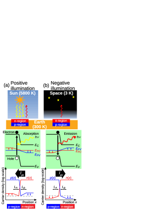
In the daytime (Fig. 1 (a)), positive illumination of light from the sun is dominant, then . The minority carriers (electrons in p-type region and holes in n-type region) increases from each equilibrium densities, respectively. The changes of the majority carriers are assumed to be negligible since the majority carrier density is much larger than the minority carrier density. Then the increment of the minority carriers makes a separation of quasi-Fermi levels for electrons in the conduction band and for holes in the valence band, while the quasi-Fermi levels of the majority carriers are almost same with the equilibrium Fermi level. The excess minority carriers diffuse to another region across the depletion layer each other. The diffusion current flowing along the n-type region to the p-type region is the photocurrent expressed by equation (1).
In the nighttime (Fig. 1 (b)), recombination rate is greater than . Under the negative illumination, electron and hole pairs disappear, and photons are emitted. To recover the decrease of the minority carriers, the majority carriers diffuse to another region across the depletion layer each other. Then the diffusion current flows along the p-type region to the n-type region. The photocurrent under negative illumination flows reverse direction to that under positive illumination.
The Wien displacement law indicates that peak of the Planck law (distribution of the photon radiation energy) of the blackbody at 300 K is at wavelength of , which is corresponding to a bandgap energy of and is in the transparent atmospheric spectral window. Therefore, an Indium Arsenide Antimonide (InAsSb) far-infrared photovoltaic device (Hamamatsu Photonics, P13894-011NA) and another mid-infrared diode (Hamamatsu Photonics, L13201-0430M) are selected for our experiment. We call former "Diode A" and later "Diode B", respectively. They are assumed to be a single p-n homo junction of a narrow direct bandgap semiconductor [15, 16]. The bandgap energy is estimated to be for Diode A, and to be for Diode B, respectively, from the maker data sheets. Area of the p-n junction is and , respectively.
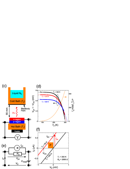
Figure 1 (c) is schematics of our experimental setup to measure the inherent photovoltaic effect under negative illumination. The infrared diodes are mounted on the Cu stage (hot bath) and its temperature is controlled by an electric heater. To avoid wavelength-dependent atmosphere absorption, we use a cold bath of Cu block cooled down by liquid nitrogen instead of real cold sky. The surface of the cold bath is coated by the blackbody painting to maximize its optical absorptance. The liquid nitrogen temperature 77 K is sufficiently cold to neglect rather than according to the Stefan-Boltzmann law (see Fig. 1 (d)). The temperature of the Diode stage and cold bathes ( and , respectively) are measured by Pt100 resistance thermometers. The diodes and the cold bath are separated in the distance of 55 mm. All of them are set in a vacuum chamber to avoid frosting on the cold bath and air convection. We measure dc voltage of the diode with a digital multimeter (Keithley 2000) or a nanovoltmeter (Keithley 2182A). Our experimental system can measure the photovoltaic effect over a wide temperature range of the diodes and that of the cold surface rather than the previous experimental researches [5, 6, 7, 8].
and are expressed as
| (2) |
and
| (3) |
respectively. Here , and are the Planck constant, the speed of light in vacuum and the Boltzmann constant, respectively. is the chemical potential of photon in emitted from nonequilibrium semiconductors [17]. The absorptivity of the semiconductor is equal to the emissivity of that according to the Kirchhoff law of thermal radiation. represents the light penetration depth of the semiconductor, and the depletion layer is assumed to be near the surface. The reason why the integrand of is proportional is that only thermal radiative photons generated inside the depth from the surface can escape outside of the semiconductor.
Figure 1 (d) shows photovoltage of Diode A at the open-circuit condition (, ) as a function of , while is kept constant. As decreases increases and is saturated to be constant because becomes negligibly small below 100 K. Furthermore. we realize that the saturated voltages for is larger than that for . This is contrary to our expectation because of a hotter object is expected to be larger than that of a colder object.
Figure 1 (e) shows the equivalent circuit of the diode. Thus the diode consists of a current source and a parallel resistance . Here the series resistance is neglected. In our measurement range, both diodes show linear I-V characteristics, as shown in Fig. 1 (f). In thermal equilibrium (), the linear curve passes through the origin. On the other hand, under the negative illumination (), the linear I-V curve moves up due to the photocurrent generation . The photocurrent and the maximum electric power generation are given by
| (4) |
where the factor 1/4 of is introduced by the maximum power transfer theorem.
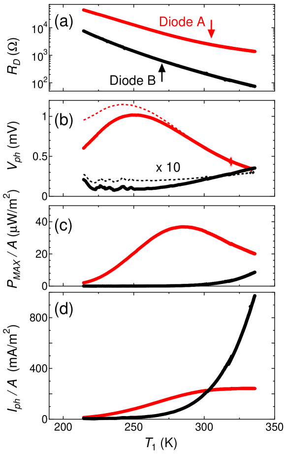
The inherent photovoltaic effect can be measured when the diode faces to a sufficiently cold bath. We keep at to , and control the diode temperature from to using an electrical heater and introducing heat exchange gas. Temperature dependences of the zero-bias resistance and the photovoltage are shown in Fig. 2 (a) and (b), respectively. is measured with the standard dc current reversal method. We note that we do not use the optical chopper [5, 6, 7], because there is difficulty to install it in our vacuum chamber. Thus the thermal electromotive force induced in the measurement circuit (see Fig. 1 (e)) by temperature difference between the diode and the voltmeter should be corrected as , where is obtained as a function of by the dark measurement (the diodes are shaded by a metal cover and performed the same cooling and heating cycle). - curve of Diode A has the maximum value (about 1 mV) at 250 K, which is consistent with the observation in Fig. 1 (d).
The maximum electrical power generation per unit area and the photocurrent per unit area are calculated by equations (4) and shown in figure 2(c) and (d), respectively. For Diode A, , and have one peak at different temperatures (indicated by red arrows in Fig. 2 (b)-(d)), although curves of both diodes show monotonically decreasing by temperature increasing. The maximum power generation of Diode A is 37 at 280 K, which is same order of the previous researches in HgTe based diodes [5, 6, 8, 7]. On the other hand, that of the Diode B shows monotonically increasing by temperature increasing. - curves of Diode B is greater than that of Diode A above 300 K, and it seems that of Diode A is suppressed above 250 K. It can be understood that the origin of the peaks of and is the suppression of .
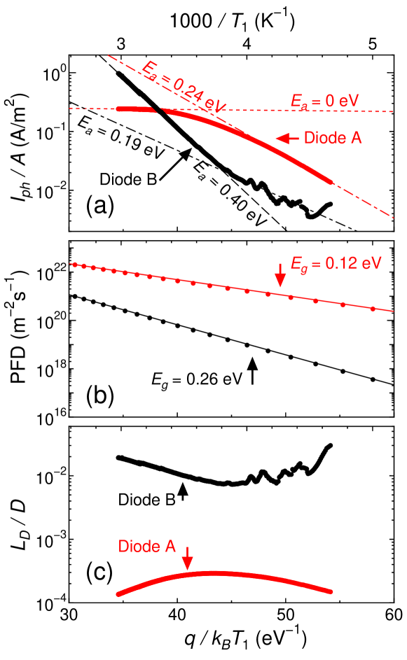
- curves of each diode are analyzed with the Arrhenius plot as shown in Fig. 3 (a). We find that both diodes have two effective activation energies depending on . The crossover temperature is 272 K for Diode A and 263 K for Diode B. Moreover, the effective activation energy of Diode A in the higher temperature range is lesser than that in the lower temperature range, however of Diode B in the higher temperature range is greater than that in the lower temperature range.
The temperature dependence of cannot be explained by temperature dependence of photon flux density (PFD), because PFD estimated by a numerical calculation with equation (3) shows monotonically increase as temperature increase [see in Fig. 3 (b)]. The curve of bandgap (the red circles and solid fitting curve) and that of (the black circles and solid fitting curve) are the models of Diode A and B, respectively. In the calculation, we assume that both and have no dependence, and for simplicity. Furthermore, the chemical potential of photon is not considered in the calculation because must be sufficiently smaller than the bandgap . Then PDF is obtained by . Both curves seem Arrhenius curves with single effective activation energy for the red curve and that with for the black curve respectively, in the temperature range of the experiment.
Finally, due to equations (1) and (3), it is found that the temperature dependence of the photocurrent depends on the diffusion length and the light penetration depth. Fig. 3 (c) indicates ratio between the diffusion length and the light penetration depth . of Diode A has a maximum at around . On the other hand, that of Diode B has minimum at around . Moreover, the ratio of Diode B is 2 order greater than that of Diode A. The difference may be determined by their device structures, such as length of light emitting layer and semiconductor materials. The light penetration depth of InAsSb is order of 10 to 100 for photon energy just above bandgap energy [18]. For , the diffusion length of Diode A is estimated to order of 10 to 100 nm. The temperature dependence of would be associated with that of the minority carrier lifetime ( and ) modified by the Auger recombination and other non-radiative recombination/excitation processes [19]. We note that the fundamental limitation due to and for the photocurrent under negative illumination has never been treated explicitly in the previous researches [10, 11, 9, 12, 13]. Their discussions treated an ideal situation that is longer than and overestimated the output power under negative illumination.
In conclusion, we investigate photovoltaic power generation of two mid-infrared diodes with different bandgap energy faced to a sufficiently cold surface. We show temperature dependence of photocurrent under negative illumination, which is inherent property in each diode. We also indicate that ratio between diffusion length of minority carriers and light penetration depth is a key parameter to increase efficiency under negative illumination. Our qualitative insight will provide a guide for development of heat-electricity conversion devices based on narrow gap semiconductors, such as near-field thermophotovoltaic energy conversion [20]. For quantitative analysis, position dependence of photon and minority carrier densities, frequency dependence of emissivity and light penetration depth, contribution of nonradiative recombination processes, and exact device structures should be considered.
Acknowledgements.
We thank M. Arakawa for fruitful discussions.References
- [1] S. J. Byrnes, R. Blanchard and F. Capasso, Harvesting renewable energy from Earth’s mid-infrared emissions PNAS, 111, 11, 3927–3932 (2014).
- [2] A. A. Penzias and R. W. Wilson, A Measurement of Excess Antenna Temperature at 4080 Mc/s, Astrophysics Journal 142, 419 (1965).
- [3] B. Bhatia, A. Leroy, Y. Shen, L. Zhao, M. Gianello, D. Li, T. Gu, J. Hu, M. Soljačić and E. N. Wang, Passive directional sub-ambient daytime radiative cooling, Nature commun., 9, 5001 (2018).
- [4] S. Assawaworrarit, Z. Omair and S. Fan, Nighttime electric power generation at a density of 50 mW/m2 via radiative cooling of a photovoltaic cell, Appl. Phys. Lett. 120, 143901 (2022).
- [5] P. Santhanam and S. Fan, Thermal-to-Electrical Energy Conversion by Diodes Under Negative Illumination, Phys. Rev. B 93, 161410(R).
- [6] M. Ono, P. Santhanam, W. Li, B. Zhao and S. Fan, Experimental demonstration of energy harvesting from the sky using the negative illumination effect of a semiconductor photodiode, Appl. Phys. Lett. 114, 161102 (2019).
- [7] M. P. Nielsen, A. Pusch, M. H. Sazzad, P. M. Pearce, P. J. Reece and N. J. Ekins-Daukes, Thermoradiative Power Conversion from HgCdTe Photodiodes and Their Current-Voltage Characteristics, ACS Photonics 9, 1535-1540 (2022).
- [8] B. Lorenzi, Y. Tsurimaki, A. Kobayashi, M. Takashiri and S. V. Boriskina, Self-powered broadband photo-detection and persistent energy generation with junction-free strained Bi2Te3 thin films Optics Express 28, 19, 27644 (2020).
- [9] X. Zhang, J. Du, J. Chen, L. K. Ang, and Y. S. Ang, Designing high-performance nighttime thermoradiative systems for harvesting energy from outer space Opt. Lett. 45, 21 (2020).
- [10] R. Strandberg, Theoretical efficiency limits for thermoradiative energy conversion J. App. Phys. 117, 055105 (2015).
- [11] C. Lin, B. Wang, K. H. Teo and Z. Zhang, Performance comparison between photovoltaic and thermoradiative devices J. Appl. Phys. 122, 243103 (2017).
- [12] W. A. Callahan, D. Feng, Z. M. Zhang, E. S. Toberer, A. J. Ferguson and E. J. Tervo, Coupled Charge and Radiation Transport Processes in Thermophotovoltaic and Thermoradiative Cells Phys. Rev. Applied 15, 054035 (2021).
- [13] H. Shibuya, N. Nagumo, K. Kugamai and A. Sakurai, Fundamental study on thermoradiative energy conversion for space applications J. Therm. Sci. and Tech. 17, 2, 22-00051 (2022).
- [14] A. S. Grove, Physics and technology of semiconductor devices, John Wiley and Sons, Hoboken, 1967.
- [15] P. K. Chiang and S. M. Bedair, p-n junction formation in InSb and InAs1-xSbx by metalorganic chemical vapor deposition, Appl. Phys. Lett. 46, 4, (1985).
- [16] K. Murawski, E. Gomółka, M. Kopytko, K. Grodecki, K. Michalczewski, Ł. Kubiszyn, W. Gawron, P. Martyniuk, A. Rogalski and J. Piotrowski, Bandgap energy determination of InAsSb epilayers grown by molecular beam epitaxy on GaAs substrates, Progress in Natural Science: Materials International 29, 472-476 (2019).
- [17] P. Würfel, The chemical potential of radiation, J. Phys. C: Solid State Phys. 15, 3967-3985 (1982).
- [18] Y. Lin, D. Donetsky, D. Wang, D. Westerfeld, G. Kipshidze, L. Shterngas, W. L. Sarney, S. P. Svensson, and G. Belenly, Development of bulk InAsSb alloys and barrier heterostructures for long-wave infrared detectors, J. Elec. Mat. 44, 10 (2015).
- [19] L. K. Casias, C. P. Morath, E. H. Steenbergen, G. A. Umana-Membreno, P. T. Webster, J. V. Logan, J. K. Kim, G. Balakrishnan, L. Faraone and S. Krishna, Vertical carrier transport in strain-balanced InAs/InAsSb type-II superlattice material Appl. Phys. Lett. 116, 182109 (2020).
- [20] R. Mittapally, A. Majumder, P. Reddy, and E. Meyhofer, Near-Field Thermophotovoltaic Energy Conversion: Progress and Opportunities, Phys. Rev. Appl. 19, 037002 (2023).