Genuine and faux single G centers in carbon-implanted silicon
Abstract
Among the wide variety of single fluorescent defects investigated in silicon, numerous studies have focused on color centers with a zero-phonon line around m and identified to a common carbon-complex in silicon, namely the G center.
However, inconsistent estimates regarding their quantum efficiency cast doubt on the correct identification of these individual emitters.
Through a comparative analysis of their single-photon emission properties, we demonstrate that these single color centers are split in two distinct families of point defects.
A first family consists of the genuine single G centers with a well-identified microscopic structure and whose photoluminescence has been investigated on ensemble measurements since the 60’s.
The remaining defects belong to a new color center, which we will refer to as G⋆ center, whose atomic configuration has yet to be determined.
These results provide a safeguard against future defect misidentifications, which is crucial for further development of quantum technologies relying on G or G⋆ center quantum properties.
The recent observation of single color centers in silicon has opened a new exploration path for silicon-based quantum technologies [1, 2, 3, 4, 5, 6, 7, 8, 9, 10, 11, 12, 13, 14, 15]. In less than three years, advanced single-defect spectroscopy has fueled the detection of more than 10 families of individual defects in silicon, able to emit non-classical, antibunched radiation in the near infrared [1, 2, 3, 4, 5, 6, 7, 9]. Surprisingly, some of these defects were not previously referenced in the extensive literature about spectroscopic measurements on defect ensembles in silicon, likely because of their relative scarcity [3]. In view of applications in the fields of single photon sources or spin-photon interfaces, it is highly desirable for a color center to possess a high radiative quantum efficiency . This value is defined as the probability after excitation to relax through photon emission rather than through a non-radiative channel. In this context, seemingly contradictory reports have been published for the G center in carbon-implanted silicon [1, 3, 8, 10, 11, 12], a defect with a zero-phonon line (ZPL) close to 1.28 µm [16, 17, 18, 19]. A remarkably high quantum efficiency has been reported in [1], while other investigations at the single defect level [8, 11] or on ensembles of G centers in optical cavities [20] point at a much smaller in the few percents range at most.
In this paper, we show that low- and high- color centers correspond to two different point defects, hereafter called G and G⋆ centers, respectively. Based on optical experiments at the single defect level, we establish the specific fingerprints of the G and G⋆ centers, and provide simple guidelines to identify them unambiguously among the wide variety of carbon-based color centers in silicon.
The experimental setup is a home-made low-temperature confocal microscope built up in a He closed-cycle cryostat (MyCryoFirm). Optical excitation of the sample is performed using a continuous laser at 532 nm and with a microscope objective (Olympus, LCPLN100XIR) mounted inside the cryostat vacuum chamber. The sample photoluminescence (PL) is collected by the same objective and measured by superconducting nanowire single-photon detectors with a detection efficiency of 78% at 1.3 m (SingleQuantum). Unless otherwise indicated, all measurements were conducted at 30K.
Single defects are investigated in two different silicon-on-insulator (SOI) samples. The first sample (#1) underwent a carbon-implantation over its entire surface at a fluence of cm-2, followed by a rapid thermal annealing during 20 s at 1,000∘C [1]. The second sample (#2) was locally implanted with carbon ions, then annealed with the same parameters as Sample #1, and at last locally irradiated with protons [6]. In Sample #2, only the lowest doses, typically cm-2 for both carbon atoms and protons, lead to densities compatible with single color center isolation [6]. Both SOI samples have a (001)-oriented top surface. The silicon top layer has a thickness of 220 nm for Sample #1 and 60 nm for Sample #2.
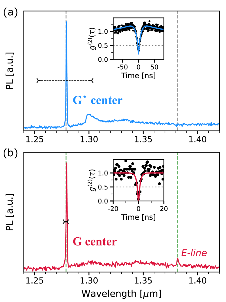
We start by examining the photoluminescence (PL) spectra of single defects evidenced by antibunching g (see Fig. 1 Insets). The spectral emission of a single color center from Sample #1 is shown in Figure 1(a). It displays a strong ZPL at 1279 nm, corresponding to the 969.45 meV referenced ZPL energy of the G center in silicon [17, 19]. A broad phonon replica with an energy of meV is also found in the PL spectrum [3]. This type of color center manifests a strong wavelength dispersion between defects: the ZPL position fluctuates in the range [1253-1303] nm (horizontal dashed line in Fig. 1(a), for a set of 41 defects, with an average value of 1273 nm and a standard deviation of 12 nm. It should be noted that, although predominant, this family of fluorescent defects coexists with other unidentified single color centers in the Sample #1 [3]. On the contrary in Sample #2, 98% of the fluorescent defects belong to the same family, connected to the typical spectrum displayed in Figure 1(b) (the remaining 2% have a broad spectrum with no detectable ZPL, similar to SD-6 defects in [3]). This emission from an individual defect also shows an intense ZPL at the reference wavelength of the G center. However, here the zero-phonon line variations between centers are much smaller. Indeed, for 39 defects, the ZPL is only found between 1277 and 1280 nm, with a mean value of 1279 nm and a standard deviation of 0.5 nm. Furthermore, an extra line is visible in the PL spectrum at 1382 nm, hence 72 meV lower than the ZPL energy. This emission line matches the E-line from the G center in silicon, associated to a local vibration mode (LVM) with a phonon energy of 71.9 meV reported in PL spectra on G-ensembles [16, 17]. It can be seen on Figure 1(a) that this E-line is not present in the PL spectrum of the individual defect from Sample #1. As a consequence, we can conclude that single color centers from Sample #2 are genuine single G centers in silicon (Fig. 1(b)). Because of their markedly different spectral signatures, namely a strong ZPL dispersion and the lack of an E-line, single defects from Sample #1 are not genuine G centers, and will be called G⋆ centers instead (Fig. 1(a)).
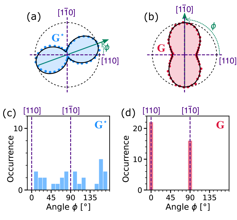
Another way to identify if a single emitter is a G or a G⋆ center is to analyze the polarization of its single photons. To this end, the emission signal of single centers is measured versus the angle of a polarizer installed before the PL collection fiber. As shown on Figure 2, two notable differences are seen on the emission polarization diagrams recorded on single G and G⋆ defects. First, the visibility of the G⋆ diagram is close to unity [1], while the one of the G diagram is typically of (Fig. 2 (a,b)). Consequently the PL of G⋆ centers comes from a single emission dipole [1], whereas the one from G centers is a result of the combination of several emission dipoles [22]. Secondly, a statistical analysis performed on individual G defects reveals that the maximum intensity is always oriented along either or crystal directions (Fig. 2 (d)). These findings are in line with former spectroscopic reports from the 80’s predicting an electric dipole along the axis [23, 16]. On the contrary, a similar study carried out on single G⋆ centers shows that their emission dipole can point in a large number of directions, except crystal axes and (Fig. 2 (c)) [1]. The orientation distribution of the emission polarization diagrams of G and G⋆ defects are thus non-overlapping, allowing to directly associate the emitters to one or the other types of defect.
Measuring the excited-state lifetime is an additional way to discriminate between G and G⋆ defects. Time-resolved measurements on single G centers show that they relax with a short timescale of roughly ns (Fig. 3(a)). This lifetime is very close to that reported on various ensembles of G centers in silicon [19, 6]. On the contrary, single G⋆ centers exhibit a much longer lifetime, typically ns, as shown in Figure 3(b) (see also Ref. [1]).
Almost one order of magnitude is also observed in the single-photon count rates between the two types of color centers. Figure 3 (b) displays the typical saturation curves recorded under continuous pumping for single G and G⋆ defects. While the G⋆ center count rate reaches 65 kcounts.s-1 for our experimental setup, the G center saturates around 7 kcounts.s-1. In spite of their longer lifetime, single G⋆ defects are thus almost 10 times brighter at saturation than the genuine single G centers. We also note that the saturation powers follow the same trend. Indeed, the signal of the G center starts to saturate for an excitation power W, while for the G⋆ defect, this occurs at W (Fig. 3 (b)).
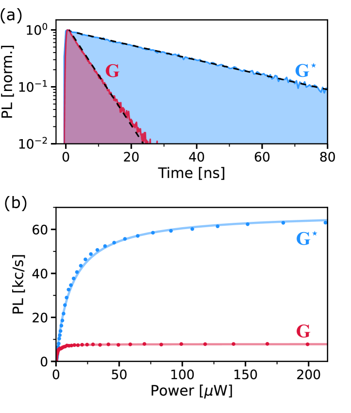
Comparing excited state lifetimes and photon count rates at saturation enables to assess the ratio of quantum efficiencies of individual G and G⋆ centers. By assuming that under continuous excitation at saturation all populations are prepared in the excited state for both defects, their respective quantum efficiencies, and , are related by the formula:
| (1) |
where are intensities at saturation and , collection efficiencies for single G and G⋆ centers, respectively (Fig. 3(b)). For a maximally collected dipole in the (001) plane, the collection efficiency varies with depth between 0.5% and 2% for the 220-nm silicon layer of Sample #1 [1] [2.5% and 4 % for the 60-nm silicon layer of Sample #2]. Considering that the brightest single defects have been selected in our experiments, the maximal value of the collection efficiency can be taken in both cases. Since the quantum efficiency of a single emitter cannot exceed 100 by definition, hence , it follows immediately that the quantum efficiency of G centers is not greater than . This low value is in agreement with previous studies [20, 8] and explains the difficulty to observe a lifetime reduction induced by the Purcell effect for these emitters [20, 11]. The quantum efficiency of single G⋆ centers is much greater. It has indeed been estimated to be at least [1].
In conclusion, we have highlighted the existence of two families of single fluorescent defects in carbon-implanted silicon that emit with a ZPL around 1.28 m. A first family consists of genuine single G centers in silicon, associated with the atomic configuration -- [24, 25, 26]. Individual G centers are unambiguously identifiable by (i) an emission spectrum containing the E-line at 1382 nm, (ii) a short excited state lifetime of 5 ns, (iii) a low quantum efficiency and (iv) a partial linear polarization but with well defined main polarization axis oriented either along or crystal axes. On the other hand, individual G⋆ centers are characterized by (i) no E-line in their PL spectrum, (ii) an excited state lifetime typically above 30 ns, (iii) a bright emission connected to a high quantum efficiency and (iv) a single emission dipole whose orientation deviates from or . Following these criteria, the single emitters investigated in [1, 2, 3, 12] are likely G⋆ centers, whereas the genuine G centers are observed in Ref. [6, 7, 10, 8, 11]. Note that the fingerprints given here for G and G⋆ centers can vary depending on their environment. For instance, a thicker top silicon layer can reduce the inhomogeneous linewidth of G⋆ centers [2] compared to our findings, and cavity integration can favor one emission dipole of the G centers as in [11].
The G center has a head start since its microscopic structure has been identified [24, 25, 26] and it can be selectively fabricated at single-defect scale through ion implantation [6, 7]. Moreover, it could host a spin qubit since a spin resonance linked to a metastable spin triplet has been detected optically on ensembles of G centers in silicon [27, 24]. In contrast, the atomic configuration of the G⋆ center is currently unknown, as well as its spin properties, and no selective fabrication method is known to date for such centers [3]. Nevertheless, its high quantum efficiency combined with single-dipole emission makes it a very promising color center to fabricate deterministic telecom single-photon sources integrated in silicon. Further investigations, including defect engineering to look for isotope shifts and ab initio calculations, are required to elucidate the G⋆ center origin and its potential connection to the G center in silicon.
Acknowledgments
We acknowledge funding from the French National Research Agency (ANR) through the projects OCTOPUS (No. ANR-18-CE47-0013-01) and QUASSIC (No. ANR-18-ERC2-0005-01), the Plan France 2030 through the project OQuLuS ANR-22-PETQ-0013, the Occitanie region through the SITEQ contract and the European Research Council (ERC) under the European Union’s Horizon 2020 research and innovation programme (project SILEQS, Grant No. 101042075). A. Durand acknowledges support from the French DGA.
References
- Redjem et al. [2020] W. Redjem, A. Durand, T. Herzig, A. Benali, S. Pezzagna, J. Meijer, A. Y. Kuznetsov, H. S. Nguyen, S. Cueff, J.-M. Gérard, I. Robert-Philip, B. Gil, D. Caliste, P. Pochet, M. Abbarchi, V. Jacques, A. Dréau, and G. Cassabois, Nature Electronics 3, 738 (2020).
- Hollenbach et al. [2020] M. Hollenbach, Y. Berencén, U. Kentsch, M. Helm, and G. V. Astakhov, Optics Express 28, 26111 (2020).
- Durand et al. [2021] A. Durand, Y. Baron, W. Redjem, T. Herzig, A. Benali, S. Pezzagna, J. Meijer, A. Kuznetsov, J.-M. Gérard, I. Robert-Philip, M. Abbarchi, V. Jacques, G. Cassabois, and A. Dréau, Physical Review Letters 126, 083602 (2021).
- Baron et al. [2022a] Y. Baron, A. Durand, P. Udvarhelyi, T. Herzig, M. Khoury, S. Pezzagna, J. Meijer, I. Robert-Philip, M. Abbarchi, J.-M. Hartmann, V. Mazzocchi, J.-M. Gérard, A. Gali, V. Jacques, G. Cassabois, and A. Dréau, ACS Photonics 9, 2337 (2022a).
- Higginbottom et al. [2022] D. B. Higginbottom, A. T. K. Kurkjian, C. Chartrand, M. Kazemi, N. A. Brunelle, E. R. MacQuarrie, J. R. Klein, N. R. Lee-Hone, J. Stacho, M. Ruether, C. Bowness, L. Bergeron, A. DeAbreu, S. R. Harrigan, J. Kanaganayagam, D. W. Marsden, T. S. Richards, L. A. Stott, S. Roorda, K. J. Morse, M. L. W. Thewalt, and S. Simmons, Nature 607, 266 (2022).
- Baron et al. [2022b] Y. Baron, A. Durand, T. Herzig, M. Khoury, S. Pezzagna, J. Meijer, I. Robert-Philip, M. Abbarchi, J.-M. Hartmann, S. Reboh, J.-M. Gérard, V. Jacques, G. Cassabois, and A. Dréau, Applied Physics Letters 121, 084003 (2022b).
- Hollenbach et al. [2022] M. Hollenbach, N. Klingner, N. S. Jagtap, L. Bischoff, C. Fowley, U. Kentsch, G. Hlawacek, A. Erbe, N. V. Abrosimov, M. Helm, Y. Berencén, and G. V. Astakhov, Nature Communications 13, 7683 (2022).
- Komza et al. [2022] L. Komza, P. Samutpraphoot, M. Odeh, Y.-L. Tang, M. Mathew, J. Chang, H. Song, M.-K. Kim, Y. Xiong, G. Hautier, and A. Sipahigil, Indistinguishable photons from an artificial atom in silicon photonics (2022), arXiv:2211.09305 [cond-mat, physics:physics, physics:quant-ph].
- Gritsch et al. [2023] A. Gritsch, A. Ulanowski, and A. Reiserer, Optica 10, 783 (2023).
- Prabhu et al. [2023] M. Prabhu, C. Errando-Herranz, L. De Santis, I. Christen, C. Chen, C. Gerlach, and D. Englund, Nature Communications 14, 2380 (2023).
- Saggio et al. [2023] V. Saggio, C. Errando-Herranz, S. Gyger, C. Panuski, M. Prabhu, L. De Santis, I. Christen, D. Ornelas-Huerta, H. Raniwala, C. Gerlach, M. Colangelo, and D. Englund, Cavity-enhanced single artificial atoms in silicon (2023), arXiv:2302.10230 [physics, physics:quant-ph].
- Redjem et al. [2023] W. Redjem, Y. Zhiyenbayev, W. Qarony, V. Ivanov, C. Papapanos, W. Liu, K. Jhuria, Z. Y. Al Balushi, S. Dhuey, A. Schwartzberg, L. Z. Tan, T. Schenkel, and B. Kanté, Nature Communications 14, 3321 (2023).
- Islam et al. [2024] F. Islam, C.-M. Lee, S. Harper, M. H. Rahaman, Y. Zhao, N. K. Vij, and E. Waks, Nano Letters 24, 319 (2024).
- Johnston et al. [2023] A. Johnston, U. Felix-Rendon, Y.-E. Wong, and S. Chen, Cavity-coupled telecom atomic source in silicon (2023), arXiv:2310.20014 [physics, physics:quant-ph].
- Lee et al. [2023] C.-M. Lee, F. Islam, S. Harper, M. A. Buyukkaya, D. Higginbottom, S. Simmons, and E. Waks, ACS Photonics 10, 3844 (2023).
- Thonke et al. [1981] K. Thonke, H. Klemisch, J. Weber, and R. Sauer, Physical Review B 24, 5874 (1981).
- Davies et al. [1983] G. Davies, E. C. Lightowlers, and M. d. Carmo, Journal of Physics C: Solid State Physics 16, 5503 (1983).
- Davies [1989] G. Davies, Physics Reports 176, 83 (1989).
- Beaufils et al. [2018] C. Beaufils, W. Redjem, E. Rousseau, V. Jacques, A. Y. Kuznetsov, C. Raynaud, C. Voisin, A. Benali, T. Herzig, S. Pezzagna, J. Meijer, M. Abbarchi, and G. Cassabois, Physical Review B 97, 035303 (2018).
- Lefaucher et al. [2023] B. Lefaucher, J.-B. Jager, V. Calvo, A. Durand, Y. Baron, F. Cache, V. Jacques, I. Robert-Philip, G. Cassabois, T. Herzig, J. Meijer, S. Pezzagna, M. Khoury, M. Abbarchi, A. Dréau, and J.-M. Gérard, Applied Physics Letters 122, 061109 (2023).
- Beveratos et al. [2002] A. Beveratos, S. Kühn, R. Brouri, T. Gacoin, J.-P. Poizat, and P. Grangier, The European Physical Journal D 18, 191 (2002).
- Durand et al. [2024] A. Durand, Y. Baron, and et al. In preparation., (2024).
- Foy et al. [1981] C. P. Foy, M. C. d. Carmo, G. Davies, and E. C. Lightowlers, Journal of Physics C: Solid State Physics 14, L7 (1981), publisher: IOP Publishing.
- O’Donnell et al. [1983] K. P. O’Donnell, K. M. Lee, and G. D. Watkins, Physica B+C 116, 258 (1983).
- Song et al. [1990] L. W. Song, X. D. Zhan, B. W. Benson, and G. D. Watkins, Physical Review B 42, 5765 (1990).
- Udvarhelyi et al. [2021] P. Udvarhelyi, B. Somogyi, G. Thiering, and A. Gali, Physical Review Letters 127, 196402 (2021).
- Lee et al. [1982] K. M. Lee, K. P. O’Donnell, J. Weber, B. C. Cavenett, and G. D. Watkins, Physical Review Letters 48, 37 (1982).