A Precision-Optimized Fixed-Point Near-Memory Digital Processing Unit for Analog In-Memory Computing
Abstract
Analog In-Memory Computing (AIMC) is an emerging technology for fast and energy-efficient Deep Learning (DL) inference. However, a certain amount of digital post-processing is required to deal with circuit mismatches and non-idealities associated with the memory devices. Efficient near-memory digital logic is critical to retain the high area/energy efficiency and low latency of AIMC. Existing systems adopt Floating Point 16 (FP16) arithmetic with limited parallelization capability and high latency. To overcome these limitations, we propose a Near-Memory digital Processing Unit (NMPU) based on fixed-point arithmetic. It achieves competitive accuracy and higher computing throughput than previous approaches while minimizing the area overhead. Moreover, the NMPU supports standard DL activation steps, such as ReLU and Batch Normalization. We perform a physical implementation of the NMPU design in a 14 nm CMOS technology and provide detailed performance, power, and area assessments. We validate the efficacy of the NMPU by using data from an AIMC chip and demonstrate that a simulated AIMC system with the proposed NMPU outperforms existing FP16-based implementations, providing 139 speed-up, 7.8 smaller area, and a competitive power consumption. Additionally, our approach achieves an inference accuracy of 86.65 %/65.06 %, with an accuracy drop of just 0.12 %/0.4 % compared to the FP16 baseline when benchmarked with ResNet9/ResNet32 networks trained on the CIFAR10/CIFAR100 datasets, respectively.
Index Terms:
Near-memory processing, Fixed-point computing, Analog in-memory computing, Deep learning, AII Introduction
The recent growth in the Artificial Intelligence (AI) domain has been driven by the shift from compute-centric systems to data-centric computing systems [1]. However, conventional von Neumann architectures exploiting data-level parallelism are bound by the memory-wall, as well as the microarchitectural challenges imposed by the increasing degree of concurrency required, which affect latency and energy efficiency [2, 3, 4]. To overcome these limitations, a promising alternative leverages non-von Neumann architectures, which perform computational tasks within the memory itself. This paradigm, known as In-Memory Computing (IMC), tackles the von Neumann bottleneck, leading to significant improvements in both energy efficiency and latency. A promising realization of IMC is Analog In-Memory Computing (AIMC), with recent works showcasing its potential [5, 6, 7]. The Matrix-Vector-Multiplication (MVM) operation, which dominates the computations (95 %) of Deep Neural Network (DNN) inference, can be performed by mapping offline-trained network weights onto AIMC tiles. Consequently, AIMC is a very promising approach for accelerating these workloads [8]. For example, a single 256256 Phase Change Memory (PCM) tile has been shown to achieve a peak energy efficiency of 10 TOPS/W [5, 6] while innovative design approaches are aiming for 100 TOPS/W [9].
A typical AIMC-tile comprises a crossbar array of memristive devices, such as PCM. The synaptic weights are programmed as the conductance value of these devices. The digital input to the tile is converted to voltage or pulse duration values using Digital-to-Analog Converters (DACs) or pulse-width modulation units, respectively, and the output from the array is converted to digital values using Analog-to-Digital Converters (ADCs). However, one key challenge is that there is substantial non-uniformity in the ADCs’ conversion behavior (or transfer curves). To address this, AIMC tiles require additional data post-processing per column through an affine correction procedure computed as:
| (1) |
where is the output of the ADC, and and are the affine correction parameters. These parameters can also be leveraged to perform any subsequent scaling and offset operation on . For instance, PCM devices exhibit significant temporal conductance drift and the conductance values also vary with temperature. These effects can be partially compensated by using correction factors [10, 11]. Moreover, the affine correction parameters can also realize Batch Normalization (BN) when implementing DNNs such as Convolutional Neural Networks (CNNs). Hence, by providing additional support for the Rectified Linear Unit (ReLU) activation function, the AIMC tile periphery provides compatibility with CNN auxiliary operations. Therefore, we formulate the operations to be performed by near-memory processing block targeting CNN implementations as follows:
| (2) |
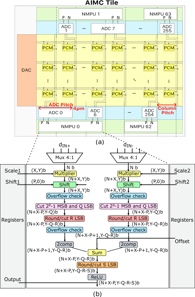
Clearly, near-memory digital processing is an indispensable part of an AIMC tile. To achieve high computational efficiency and low latency in AIMC systems, it is desirable to integrate the custom near-memory digital logic circuitry for each crossbar column. However, maximizing the area efficiency of the tile (TOPS/mm2), as well as complying with the small pitch of the AIMC columns and the ADCs (for instance, 4 m in [5]), heavily constraints the available area budget and the physical implementation of this block (Fig. 1a). Therefore, a flexible solution maintaining high energy efficiency and accuracy while being compact and fast is required. Designs using Floating Point 16 (FP16) datatypes were explored in prior works [5, 6]. However, these approaches incur a relatively large area and power consumption. This leads to a large digital block shared across multiple columns (e.g., 256 columns in [6]), which limits parallelization and requires serial pipelined processing for all outputs. An alternative is the adoption of standard integer types, which reduce the area overhead and enable multiplexing across 8 [12] or 16 [13] crossbar columns.
In this paper, we address the limitations of existing solutions by proposing a flexible Near-Memory digital Processing Unit (NMPU) that leverages fixed-point precision computation to perform accurate affine correction and auxiliary operations while minimizing its area footprint. Our design can be multiplexed across just 4 memristive crossbar array columns and, compared to [12, 13], adopts truncation and rounding schemes, significantly reducing the size of intermediate representations for a more compact design. We experimentally validate the effectiveness of our approach using ADC data from a PCM-based AIMC chip [5].
II NMPU microarchitecture and design space exploration
The NMPU microarchitecture implementing the computations of (2) is shown in Fig. 1b. The design consists of two identical branches, which apply different scale parameters to the digitized values of positive and negative currents coming from one ADC as distinct paths [5, 6]. The block consumes two 10-bit unsigned integer inputs and produces an 8-bit signed output. In addition, the unit implements rounding and truncation steps to reduce intermediate precision and mitigate precision loss during the computations. The design is fully parameterizable in terms of the inputs, scale, shift and offset factors, intermediate truncation formats, and output format. In the following, we explore optimal parameters for the proposed block. For this analysis, we set the input and output formats as 10-bit unsigned (integer) and 8-bit signed (2’s complement), respectively. The choice of the input format is based on the adoption of a 10-bit ADCs’ design, while 8-bit outputs for activations are widely adopted for Deep Learning (DL) inference acceleration [14, 4, 15, 16, 17].
First, we determine the optimal data formats for scale and offset constants by analyzing the ADC transfer curves, which are experimentally acquired from circuit measurements of [5] and shown in Fig. 2.
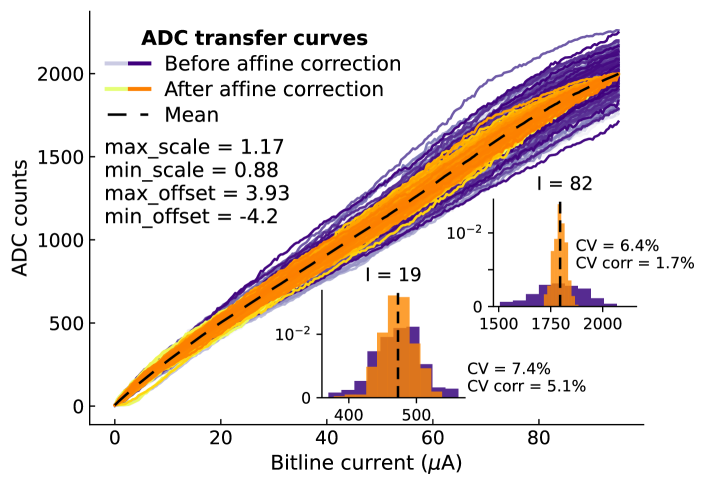
They are obtained for a set of 256 distinct ADCs after being properly calibrated [5]. The individual trajectories highlight the variations across individual ADCs, and the relationship between the bit-line current and the converted ADC counts is observed to be nonlinear. The affine correction (see (1)) minimizes the variation of the curves with respect to their mean, i.e., tuning the slope with a certain precision granularity. We estimate the maximum and minimum scaling factors for the affine correction as 0.88 and 1.17, respectively. Hence, 1-bit for the integer part is sufficient in the corresponding fixed-point number. On the other hand, the fractional part depends on the desired precision for the tuning, which is targeted to be higher than the precision of the Coefficient of Variation (CV) in the set of 256 ADCs transfer curves. Since the CV is observed to be 7 % of the mean, we retain a granularity of 1 %, which corresponds to , i.e., 7-bit. Thus, we need 1-bit and 7-bit to represent the integer and fractional part of the scale parameter, respectively, i.e., (1,7) bit unsigned. For the offset parameter, we observe that (4,0) bit signed is sufficient to account for the measured offset. However, we allocate more bits to accommodate for any further requirement associated with the BN operation and propose using (7,1) bit signed.
To perform the scaling in high precision and to ensure that the scaled values fit the output range, we introduce a right shift operation after the scale (see Fig. 1b). Given that the ADCs’ output precision is 10-bit unsigned, the scale is 1-bit precision for the integer part, and the output is 8-bit signed, the maximum value needed for the right shift is three, which can be represented with 2 bits. In addition, since the shift operation ensures the range fits 8-bit, we reduce the integer bits by cutting the unused Most Significant Bits (MSBs), i.e., () MSBs. Furthermore, since a high degree of precision is unnecessary when determining the methodology for conducting the rounding operation, we truncate the Least Significant Bits (LSBs) up to and including .
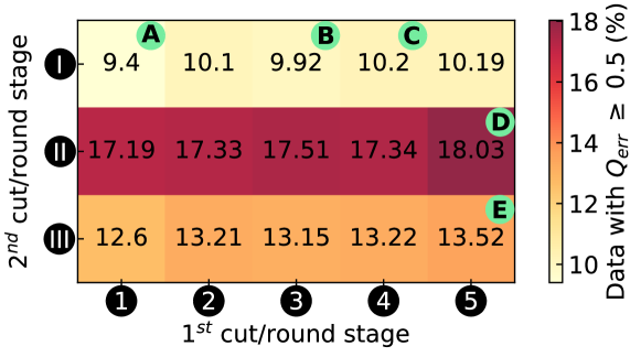
To evaluate the influence of cut and round operations on the overall precision loss, we consider 15 distinct architectures leveraging a different combination of cut/round methods after the scaling (first cut/round stage) and the sum (second cut/round stage). We denote as guard (G) and round (R) the bits that determine whether a truncation or rounding should occur, respectively, and as x the bits not affecting the decision. For the first cut/round stage, we consider five methods: cut 3 LSBs up to (excluded) and round only looking at the bit at position (x.xxRxx); cut 3 LSBs up to (excluded) and if the bit at position is 1 then we cut; otherwise, we round looking at the bits at position or (if at least one is 1) (x.xGRRx); cut 3 LSBs up to (excluded) and if the bit at position is 1 then we cut; otherwise, we round looking at the bit at position (x.xGRxx); cut 3 LSBs up to (excluded) and if the bit at position is 1 then we cut; otherwise, we round looking at the bit at position or or (x.xGRRR); cut 3 LSBs up to (excluded) (x.xxxxx).
For each of these methods, we consider three ways of performing the second cut/round stage: cutting the LSB for both positive and negative values; rounding the LSB for positive and cutting LSB for negative values; and rounding LSB for both positive and negative values.
III Evaluating precision of the proposed datapath
To evaluate the impact of the two cut/round stages on the precision loss, we evaluate the architectures with a cycle-accurate Register Transfer Level (RTL) simulator, using randomly generated data from a univariate normal Gaussian distribution with mean 0 and variance 1 for the inputs. As an evaluation metric for the precision loss, we compute the quantization error against a software-based (FP32) baseline:
| (3) |
Being the output integer, the best architectures provide the lowest percentage of data with , as shown in Fig. 3. We observe that is mainly affected by the method adopted for the second cut/round stage. In particular, the architectures implemented with have less than 11 % of data (over a range of 10,000 data points) with . We continue the analysis by selecting the two most performant architectures (A and B), as well as the least performant for each method in the second cut/round stage (C, D and E), as shown in Fig. 3.
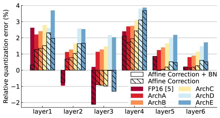
Next, we implement Python models for the selected architectures and evaluate them using ADC data from the chip presented in [5]. Data is extracted during inference on a modified ResNet9 model [18]. We compare the relative quantization error on a layer-by-layer basis (i.e., without any layer propagation) with the software baseline. More specifically, the error per layer is evaluated as follows. First, we compute the MVM and, where applicable, the BN, all in FP32, to serve as a software baseline. Second, we estimate the hardware operation error (“hw_op_err”) resulting from performing both MVM and analog-to-digital conversion on chip when the affine correction and BN are performed in FP32 (AIMC-baseline). This hardware operation error is computed as the root-mean-squared (L2) error between the AIMC-baseline and the software baseline results. Then, we estimate the L2-error between the software baseline and the proposed implementations (referred to as “impl_err”), where the MVM is performed on-chip and the affine correction and BN are performed with the selected NMPU variants. Finally, the relative quantization error is calculated as:
| (4) |
Fig. 4 shows that the NMPU block incurs a relative quantization error 4 % and 2 % compared to the AIMC-baseline and to the FP16-based post-processing implementation from [5] for all layers, respectively. When including BN, increases for both the NMPU and the FP16 compared to the AIMC-baseline. In both situations, NMPU’s varies with a trend similar to that of Fig. 3. In the best case, i.e., ArchA, the NMPU achieves a 1 % compared to FP16. Consequently, in circuit applications, where the absolute value on the output is crucial, exploring different cut/round methods is important to identifying the architecture with the lowest output error. However, when targeting DL applications, the final goal is the accuracy assessment rather than comparing absolute output values. Therefore, in the following, we investigate the impact of the quantization error on the accuracy evaluation, building towards a more comprehensive application study.
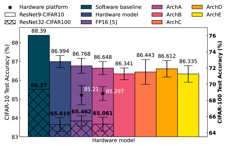
Besides the previous evaluation, we feed the output of the near-memory post-processing block to the AIMC tile containing the weights of the subsequent layer. For this study, we simulate the hardware using statistical models extracted from chip measurements [6] and explore both ResNet9 and a deeper ResNet32 [19] on the CIFAR10 and CIFAR100 datasets, respectively. Fig. 5 shows the results obtained via simulations. We observe an accuracy degradation from the software baseline (similar to that of Fig. 4) when the hardware model is used. The hardware model employs statistical models of the chip to simulate the MVM and data converters, while the affine correction and BN are performed in FP32. In the other implementations from Fig. 5, the hardware model is revised to perform the affine correction and BN using FP16 [5] or the proposed NMPUs. For ResNet9 on the CIFAR10 dataset, the selected architectures show an inference accuracy drop 2.1 % compared to the software baseline, 0.7 % compared to the hardware model with an FP32 periphery, and 0.5 % compared to the FP16 [5] model. Overall, independently of the observed , the fixed-point-based NMPUs do not significantly affect the inference accuracy, whose degradation is instead dominated by the MVM non-idealities.
Since the accuracy of the explored architectures is similar, for ResNet32 on the CIFAR100 dataset and for the following explorations, we consider only the architecture with the highest inference accuracy mean, i.e. 86.648 %, referred to as ArchA. Fig. 5 shows that, ArchA, achieves an inference accuracy of 86.648 %/65.061 % on the CIFAR10/CIFAR100 dataset, with an accuracy drop of only 0.12 %/0.4 % compared to an FP16-based near-memory logic.
To enhance the consistency of our study, the NMPU based on ArchA has been integrated into the software stack of the hardware platform proposed by [5], enabling chip-in-the-loop simulation. The existing FP16-based near-memory logic has been disabled from the physical chip. The chip is linked with the software environment where the NMPU is implemented through a communication infrastructure that allows them to interact for the computation of subsequent layers. Fig. 5 shows the results for ResNet9 trained on CIFAR10 dataset when using a real hardware platform (marked with a star in the figure). As the previous simulations did not account for all chip non-idealities, the real-hardware experiments show an accuracy degradation compared to software simulations. Nonetheless, the proposed fixed-point NMPU implementation achieves competitive performance compared to the FP16-based system, consistent with the simulation results. To fully exploit the benefits of adopting a flexible fixed-point-based architecture, in the next section, we detail its physical implementation and power, performance and area (PPA) assessment.
IV Synthesis of NMPU in 14nm CMOS technology
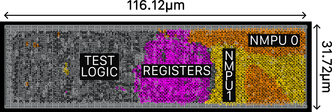
We synthesize ArchA using Cadence Genus 20.11 and perform physical implementation using Cadence Innovus 21.13 in a 14 nm CMOS technology. The resulting PPA estimations are shown in Table I. The NMPU results in a 505 area reduction compared to FP16 [5], whose area is estimated to be about 1.67 MGE (Gate Equivalent). The significant area reduction enables to time-multiplex the NMPU across 4 columns of architectures with an ADC pitch of 4 m, e.g. [5, 6]. Therefore, the lean design allows fitting 64 NMPUs operating in parallel in such systems. The resulting latency and power consumption for post-processing of an AIMC core [5] read 4 ns and 24.5 mW, respectively. This implies that the proposed approach is 139 faster than FP16 [5], which requires about 558 ns to process all the 256 outputs in a serial-pipelined fashion. The micrograph of the unit, including two fixed-point-based NMPUs, the configuration registers for the scale and offset parameters, and the test interface is shown in Fig. 6.
| System | Area (kGE) | Latency (ns) | Tot Latency (ns) | Power (mW) | |
| SS | FF | ||||
| ArchA | 3.3 | 1 | 256 | 0.383 | 0.524 |
| ArchA64 | 211 | 1 | 4 | 24.5 | 33.5 |
| FP16 [5] | 1666 | 46 | 558 | 27 (post-layout=32) | |
V Conclusion
In this paper, we proposed a fixed-point NMPU designed, simulated, and physically implemented using 14 nm CMOS technology. Our NMPU achieves competitive precision on both small and large networks, i.e., ResNet9 and ResNet32, with accuracy drops of only 0.12 % and 0.4 % compared to existing AIMC solutions adopting FP16 precision while minimizing the area overhead by 505 . Furthermore, due to NMPU’s compact form factor, we proved its high-parallelization capability by fitting 64 fixed-point based NMPUs in a 7.8 smaller area than the FP16-based implementation of [5]. This results in a 139 speed-up for the whole post-processing computation without increasing the power consumption.
VI Acknowledgments
We thank M. Ishii and M. Brändli for technical support. This work was supported by IBM Research AI Hardware Center, European Union’s Horizon Europe Research and Innovation Program (Grant 101070634), and Swiss State Secretariat for Education, Research and Innovation (SERI) (Grant 23.00205).
References
- [1] Siegl, Patrick & Buchty, Rainer & Berekovic, Mladen. (2016). “Data-Centric Computing Frontiers: A Survey On Processing-In-Memory.” 295-308.
- [2] S. W. Keckler, W. J. Dally, B. Khailany, M. Garland and D. Glasco, “GPUs and the Future of Parallel Computing,” in IEEE Micro, vol. 31, no. 5, pp. 7-17, Sept.-Oct. 2011.
- [3] Jouppi, Norman P., et al. “In-Datacenter Performance Analysis of a Tensor Processing Unit.” Proceedings of the 44th Annual International Symposium on Computer Architecture, June 2017. Crossref.
- [4] V. Sze, Y. -H. Chen, T. -J. Yang and J. S. Emer, “Efficient Processing of Deep Neural Networks: A Tutorial and Survey,” in Proceedings of the IEEE, vol. 105, no. 12, pp. 2295-2329, Dec. 2017.
- [5] R. Khaddam-Aljameh et al., “HERMES-Core—A 1.59-TOPS/mm2 PCM on 14-nm CMOS In-Memory Compute Core Using 300-ps/LSB Linearized CCO-Based ADCs,” in IEEE Journal of Solid-State Circuits, vol. 57, no. 4, pp. 1027-1038, April 2022.
- [6] Le Gallo, M., Khaddam-Aljameh, R., Stanisavljevic, M. et al. “A 64-core mixed-signal in-memory compute chip based on phase-change memory for deep neural network inference.” Nat Electron 6, 680–693 (2023).
- [7] Wan, W., Kubendran, R., Schaefer, C. et al. “A compute-in-memory chip based on resistive random-access memory.” Nature 608, 504–512 (2022). https://doi.org/10.1038/s41586-022-04992-8
- [8] Sebastian, A., Le Gallo, M., Khaddam-Aljameh, R. et al. “Memory devices and applications for in-memory computing.” Nat. Nanotechnol. 15, 529–544 (2020).
- [9] S. Jain et al., “A Heterogeneous and Programmable Compute-In-Memory Accelerator Architecture for Analog-AI Using Dense 2-D Mesh,” in IEEE Transactions on Very Large Scale Integration (VLSI) Systems, vol. 31, no. 1, pp. 114-127, Jan. 2023.
- [10] S.R., Nandakumar & Boybat, Irem & Han, Jin-Ping & Ambrogio, Stefano & Adusumilli, Praneet & Bruce, Robert & BrightSky, Matthew & Rasch, Malte & Gallo, Manuel & Sebastian, Abu. (2020). “Precision of synaptic weights programmed in phase-change memory devices for deep learning inference.” 29.4.1-29.4.4.
- [11] Boybat, Irem & Kersting, B. & Sarwat, S. & Timoneda, X. & Bruce, R. & BrightSky, M. & Gallo, M. & Sebastian, A.. (2021). “Temperature sensitivity of analog in-memory computing using phase-change memory.” 28.3.1-28.3.4.
- [12] H. Jia et al., “Scalable and Programmable Neural Network Inference Accelerator Based on In-Memory Computing,” in IEEE Journal of Solid-State Circuits, vol. 57, no. 1, pp. 198-211, Jan. 2022.
- [13] H. Jia, H. Valavi, Y. Tang, J. Zhang and N. Verma, “A Programmable Heterogeneous Microprocessor Based on Bit-Scalable In-Memory Computing,” in IEEE Journal of Solid-State Circuits, vol. 55, no. 9, pp. 2609-2621, Sept. 2020.
- [14] Jouppi, Norman & Borchers, Al & Boyle, Rick & Cantin, Pierre-luc & Chao, Clifford & Clark, Chris & Coriell, Jeremy & Daley, Mike & Dau, Matt & Dean, Jeffrey & Gelb, Ben & Young, Cliff & Ghaemmaghami, Tara & Gottipati, Rajendra & Gulland, William & Hagmann, Robert & Ho, C. & Hogberg, Doug & Hu, John & Boden, Nan. (2017). “In-Datacenter Performance Analysis of a Tensor Processing Unit.” 1-12.
- [15] Y. -H. Chen, T. -J. Yang, J. Emer and V. Sze, “Eyeriss v2: A Flexible Accelerator for Emerging Deep Neural Networks on Mobile Devices,” in IEEE Journal on Emerging and Selected Topics in Circuits and Systems, vol. 9, no. 2, pp. 292-308, June 2019.
- [16] The Next Platform, “Nvidia Pushes Deep Learning Inference With New Pascal GPUs”, Sept 2016, https://www.nextplatform.com/2016/09/13/nvidia-pushes-deep-learning-inference-new-pascal-gpus/
- [17] A. Reuther, P. Michaleas, M. Jones, V. Gadepally, S. Samsi and J. Kepner, “AI and ML Accelerator Survey and Trends,” 2022 IEEE High Performance Extreme Computing Conference (HPEC), Waltham, MA, USA, 2022, pp. 1-10.
- [18] J. Büchel et al., “Gradient descent-based programming of analog in-memory computing cores,” 2022 International Electron Devices Meeting (IEDM), San Francisco, CA, USA, 2022, pp. 33.1.1-33.1.4.
- [19] K. He, X. Zhang, S. Ren and J. Sun, “Deep Residual Learning for Image Recognition,” 2016 IEEE Conference on Computer Vision and Pattern Recognition (CVPR), Las Vegas, NV, USA, 2016, pp. 770-778.