Tuning proximity spin-orbit coupling in graphene/NbSe2 heterostructures via twist angle
Abstract
We investigate the effect of the twist angle on the proximity spin-orbit coupling (SOC) in graphene/NbSe2 heterostructures from first principles. The low-energy Dirac bands of several different commensurate twisted supercells are fitted to a model Hamiltonian, allowing us to study the twist-angle dependency of the SOC in detail. We predict that the magnitude of the Rashba SOC can triple, when going from to twist angle. Furthermore, at a twist angle of the in-plane spin texture acquires a large radial component, corresponding to a Rashba angle of up to . The twist-angle dependence of the extracted proximity SOC is explained by analyzing the orbital decomposition of the Dirac states to reveal with which NbSe2 bands they hybridize strongest. Finally, we employ a Kubo formula to evaluate the efficiency of conventional and unconventional charge-to-spin conversion in the studied heterostructures.
I Introduction
Combining different 2D materials into one heterostructure held together by van der Waals forces has become a well trodden path of engineering new physics Geim and Grigorieva (2013); Duong et al. (2017); in this approach, the materials can imprint some of their own properties onto another by proximity effects. Graphene has been the most researched material in this context, since it provides high electron mobility Bolotin et al. (2008); Du et al. (2008) and long spin-relaxation times Singh et al. (2016); Drögeler et al. (2016). Embedding it into a heterostructure can enhance its spin-orbit coupling Gmitra and Fabian (2015); Gmitra et al. (2016); Wang et al. (2015a); Avsar et al. (2014); Naimer et al. (2021); Naimer and Fabian (2023); Zollner et al. (2023) (e.g. graphene/WSe2), equip it with magnetic properties Karpiak et al. (2019); Wang et al. (2015b); Wei et al. (2016); Zhang et al. (2015); Zollner et al. (2018); Zhang et al. (2018) (e.g. graphene/Cr2Ge2Te6) or turn it into a superconductor Gani et al. (2019); Moriya et al. (2020); Zhang et al. (2020) (e.g. graphene/NbSe2).
Although graphene/NbSe2 is mostly studied in the context of superconducting graphene Wang et al. (2017); Xi et al. (2016); Khestanova et al. (2018); Gani et al. (2019); Moriya et al. (2020); Zhang et al. (2020), the spin-orbit coupling of graphene is expected to be enhanced in such heterostructures as well. This is because NbSe2 has a large spin-orbit coupling, similar to semiconducting transition-metal dichalcogenides (TMDCs). In heterostructures of graphene and semiconducting TMDCs (e.g., WSe2), the influence of the twist angle on the proximity SOC was found to be of great impact: Not only does the magnitude and type of SOC vary, but also a radial component is introduced to the in-plane spin structure for non-zero twist angles, as studied by tight binding models Li and Koshino (2019); David et al. (2019); Péterfalvi et al. (2022) and ab initio simulations Naimer et al. (2021); Lee et al. (2022); Zollner et al. (2023). Recently, the emergence of a radial component of the Rashba spin-orbit field was confirmed experimentally Yang et al. (2023). However, unlike graphene heterostructures based on semiconducting TMDCs which feature Dirac points within the semiconductor band gap, in graphene/NbSe2 the Dirac point lies within the metallic bands of NbSe2. This brings certain challenges for deciphering the proximity effects, making their first-principles investigations useful for understanding the interplay between SOC and superconductivity Gani et al. (2019); Moriya et al. (2020); Zhang et al. (2020) and for charge-to-spin conversion in graphene/NbSe2 heterostructures Ingla-Aynés et al. (2022). Particularly the collinear charge-to-spin conversion (unconventional Rashba Edelstein effect, UREE Ingla-Aynés et al. (2022); Péterfalvi et al. (2022); Veneri et al. (2022); Lee et al. (2022); Camosi et al. (2022); Ontoso et al. (2023); Yang et al. (2023)) as opposed to the more usual perpendicular charge-to-spin conversion (Rashba Edelstein effect, REE Ghiasi et al. (2017); Offidani et al. (2017); Dyrdał et al. (2014); Edelstein (1990)) has a high potential for being realized in these heterostructures. Since all SOC parameters (and especially the Rashba phase angle , linked to collinear charge-to-spin conversion) can vary strongly with the twist angle as shown for graphene/TMDCs Naimer et al. (2021); Lee et al. (2022); Zollner et al. (2023); Li and Koshino (2019); David et al. (2019); Péterfalvi et al. (2022); Yang et al. (2023); Kiemle et al. (2022) and graphene/topological insulators Zhang et al. (2014); Song et al. (2018); Naimer and Fabian (2023) , it is important to uncover such dependencies for graphene/NbSe2 heterostructures as well.
To predict twist-angle dependence of proximity SOC, we perform density functional theory (DFT) calculations on several commensurate graphene/NbSe2 supercells. We fit the obtained band structures around the Dirac points to a model Hamiltonian which comprises different SOC terms. The main result of the paper are the extracted SOC values depending on the twist angle . More specifically, we find that valley Zeeman and Rashba SOC both have a magnitude of just under 1 meV for twist angles . Then, for , the Rashba SOC steadily increases reaching a maximum of about 2.5 meV at , while the valley Zeeman SOC steadily decreases to zero magnitude at . At , the Rashba phase angle has a maximum with a value of .
Furthermore, we explicitly investigate the potential of the different graphene/NbSe2 supercells for charge-to-spin conversion. By using the Kubo formula in the Smrcka-Streda formulation, we evaluate at what twist angles the potential for measuring REE or UREE is the highest. Our findings support the intuitive picture following from the SOC parameters: the highest yield for REE is possible for (maximal Rashba SOC, minimal valley-Zeeman SOC). The highest yield for UREE is possible for (maximal Rashba phase angle , high Rashba SOC).
The paper is structured as follows: In Sec. II we show the supercells used for the DFT calculations and the model Hamiltonian used for the fitting. Sec. III discusses the band alignments and the challenges linked to the metallic nature of the NbSe2. In Sec. IV, the twist-angle dependence of the proximity SOC parameters is presented. The potential for charge-to-spin conversion is explored in Sec. V within linear response theory. In App. A and App. B the effects of an external electric field and relaxation are discussed respectively. Finally, in App. C we present some details on the calculations done in Sec. V.
II Structures and methods
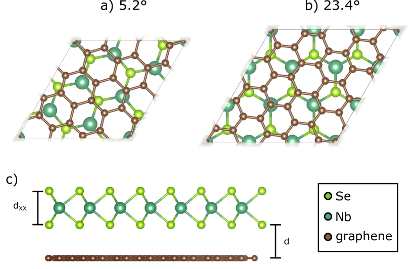
Combining monolayer graphene (lattice constant Å) and a monolayer of NbSe2 (lattice constant Å Ding et al. (2011) and thickness Å Gani et al. (2019)), we construct the supercells listed in Tab. 1 implementing the coincidence lattice method (Koda et al., 2016; Carr et al., 2020). The chosen interlayer distance (we study the effects of structural relaxation in App. B) is Å. The integer attributes determine the lattice vectors of the (graphene or NbSe2) supercell
| (1) | ||||
| (2) |
where and are the primitive lattice vectors (of graphene or NbSe2). These new supercell lattice vectors in turn determine the twist angle and strain of the heterostructure (for details on this notation, see Naimer et al. (2021)). Two examples of such heterostructures are shown in Fig. 1. Assuming that the lateral degree of shifting plays a minor role for larger supercells (see Ref. Naimer et al. (2021); Naimer and Fabian (2023)), we use the convention of a shifting position where at the corner of the supercell a Nb atom sits on top of a C atom. In order to achieve a commensurate heterostructure suitable for DFT calculations, we need to introduce the strain in either the NbSe2 or the graphene. Since graphene’s electronic structure is less affected by strain, we choose to put all the strain on graphene and leave the NbSe2 unstrained. Finally, we add a vacuum of 20 Å to avoid interactions between periodic images in our slab geometry. Electronic structure calculations are then performed by density functional theory (DFT) (Hohenberg and Kohn, 1964) with Quantum ESPRESSO (Giannozzi and et al., 2009).
| [%] | ||||
|---|---|---|---|---|
| 0.00000 | ( 0 4 ) | ( 0 3 ) | 6.0976 | 59 |
| 0.00000 | ( 7 0 ) | ( 5 0 ) | 1.0453 | 173 |
| 1.87177 | ( 3 4 ) | ( 2 3 ) | 1.3725 | 131 |
| 3.30431 | ( 6 1 ) | ( 4 1 ) | -1.1402 | 149 |
| 5.20872 | ( 3 1 ) | ( 2 1 ) | 3.8058 | 47 |
| 5.20872 | ( 2 4 ) | ( 1 3 ) | -3.6090 | 95 |
| 8.94828 | ( 1 5 ) | ( 0 4 ) | 1.6303 | 110 |
| 10.89339 | ( 2 1 ) | ( 1 1 ) | -7.3905 | 23 |
| 11.30178 | ( 4 3 ) | ( 2 3 ) | 1.3725 | 131 |
| 12.51983 | ( 7 1 )* | ( 4 2 ) | -0.8516 | 198 |
| 13.89789 | ( 2 6 ) | ( 0 5 ) | -1.9128 | 179 |
| 13.89789 | ( 5 0 ) | ( 3 1 ) | 2.0107 | 89 |
| 16.10211 | ( 6 2 ) | ( 3 3 ) | 1.9352 | 185 |
| 16.10211 | ( 3 3 )* | ( 1 3 ) | -1.8401 | 93 |
| 19.10661 | ( 4 0 ) | ( 2 1 ) | -6.4308 | 53 |
| 19.10661 | ( 1 2 ) | ( 0 2 ) | 6.9363 | 26 |
| 20.48466 | ( 5 2 )* | ( 2 3 ) | -1.2610 | 135 |
| 23.41322 | ( 2 3 ) | ( 0 3 ) | -2.6382 | 65 |
| 26.99551 | ( 4 2 ) | ( 1 3 ) | -3.6089 | 95 |
| 26.99551 | ( 3 1 ) | ( 1 2 ) | 3.8058 | 47 |
| 30.00000 | ( 5 0 ) | ( 2 2 ) | -1.9913 | 86 |
| 30.00000 | ( 4 4 )* | ( 0 5 ) | 2.0924 | 171 |
To quantify the proximity induced SOC in graphene’s Dirac bands due to the coupling with the NbSe2 monolayer, we fit the DFT band structures at the Dirac points to a model Hamiltonian (Gmitra and Fabian, 2015). The Hamiltonian comprises the orbital part and the spin-orbit part . The latter is composed of the intrinsic spin-orbit coupling and the Rashba coupling :
| (3) |
The orbital part describes the dispersion of the graphene Dirac cone; it is linearized around the /-point, therefore is the electron wave vector measured from /. It also includes a staggered potential , taking into account any asymmetrical influence of the NbSe2 substrate on the graphene A- and B-sublattice:
| (4) |
Here, is the Fermi velocity of the Dirac electrons and and are the Pauli matrices operating on the sublattice (A/B) space. The parameter determines, whether the Hamiltonian describes the band structure near K or K’ ( for and for ).
The intrinsic spin-orbit Hamiltonian
| (5) |
and the Rashba spin-orbit Hamiltonian
| (6) |
both include spin Pauli matrices and acting on the spin space; and are the valley-Zeeman (Gmitra and Fabian, 2015; Wang et al., 2015a) SOC (sublattice-odd) and the Kane-Mele (Kane and Mele, 2005) SOC (sublattice-even) respectively. The Rashba SOC term is defined by two parameters: the magnitude and the phase angle . The latter is present in symmetric structures (Li and Koshino, 2019; David et al., 2019; Naimer et al., 2021) and rotates the spin texture about the -axis, adding a radial component to the Rashba field.
We only construct heterostructures with angles between 0° and 30°. The parameters for all other twist angles can be obtained by the following symmetry rules:
| (7) | ||||
| (8) | ||||
| (9) | ||||
| (10) | ||||
| (11) | ||||
| (12) | ||||
| (13) | ||||
| (14) |
We note that NbSe2 exhibits charge density wave (CDW) Ugeda et al. (2016); Xi et al. (2015); Lian et al. (2018). In App. B, we discuss a typical CDW in NbSe2 with the same atomic rearrangement in the heterostructure with graphene. Since the CDW does not significantly influence the proximity SOC in graphene, in the main text we perform simulations on unrelaxed structures to facilitate systematic comparison between different twist angles.
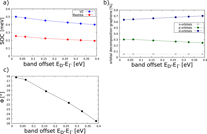
For DFT calculations of heterostructures, the varying band offsets induced by strain (see Sec. III) can be relevant for the extracted SOC parameters. In Refs. Naimer et al. (2021); Naimer and Fabian (2023) we used electric fields to correct for the strain-induced band offsets. However, in this paper we use only supercells with built-in strain for the determination of the SOC parameters. Therefore, we find a much lower variance in band offsets and hence rather follow the approach of Refs. Lee et al. (2022); Zollner et al. (2023) and deem these corrections unnecessary. In App. A we explore how a transverse electric field can influence the SOC parameters and orbital contributions for one particular example. Our findings indicate that the electric field’s main effect is a change of the Rashba phase angle .
III Energetic alignments
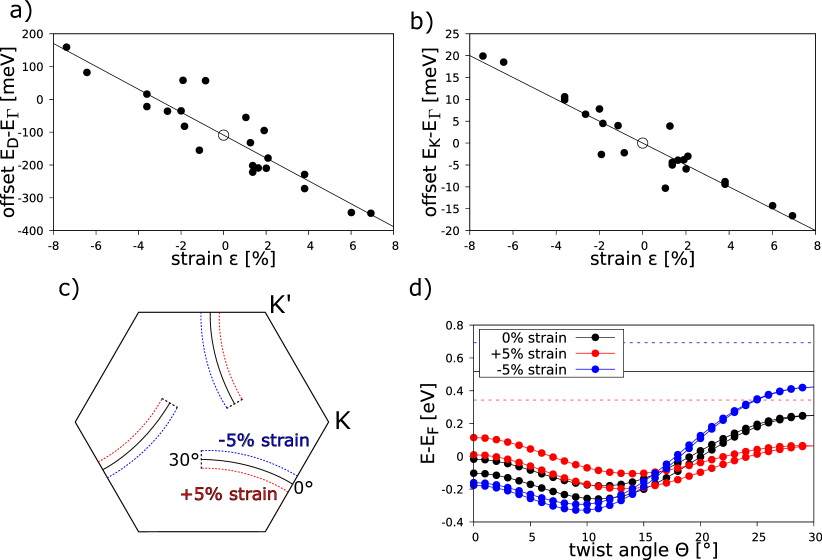
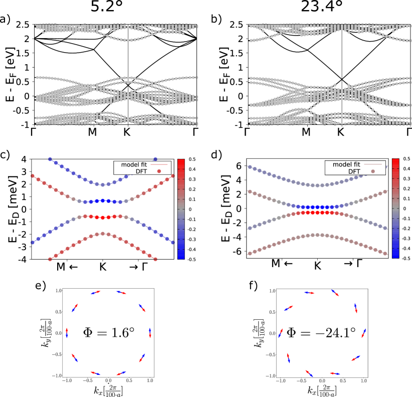
We calculate the band structures of our supercell graphene/NbSe2 heterostructures using DFT. Two examples can be seen in Fig. 3 a) and b). In contrast to semiconducting graphene/TMDC heterostructures (Ref. Naimer et al. (2021); Gmitra and Fabian (2015)) the graphene Dirac cone (solid black lines) lies buried within the NbSe2 bands (grey bands) for most cases. However, in some cases the Dirac cone lies above these bands. To better describe the energetic alignments we define the band offsets as follows: and are the band edges of the NbSe2 states near the Fermi level at and respectively. is the energy level of the Dirac cone. In Fig. 2 a) we show the (approximately linear) relation between the strain in graphene and the band offset . If this band offset is positive, the Dirac cone lies above the NbSe2 bands. By applying a linear fit we can extract a zero-strain band offset meV. Defining the band offset as would yield very similar results. Nevertheless, we need to distinguish between and because the NbSe2 band structure also changes by the proximity of the graphene. In fact, we see a similar behaviour (linear with strain , see Fig. 2 b)) of the internal band offset . Depending on , this band offset can also be negative or positive. This can be interpreted in the following way: Compressing the graphene () creates a more dense barrier of graphene orbitals pushing the (out-of-plane orbital dominated) NbSe2 bands further down in energy than the (more in-plane) bands.
Although for most of the heterostructure supercells the Dirac cone lies within the NbSe2 bands, this does not necessarily mean that the Dirac cone hybridizes with NbSe2 bands in a way that makes it impossible to describe the Dirac cone with our model Hamiltonian. The reason for this is that the NbSe2 bands, which are energetically close to the Dirac cone, hardly interact with it. Following the theory of generalized Umklapp processes Koshino (2015) the bands interacting the most with the Dirac cone are energetically well separated from it. This is illustrated in Fig. 2 c) and d): Depending on strain and twist angle, the Dirac cone interacts with a different point in the first Brillouin zone of the primitive NbSe2 (shown in Fig. 2 c)). We are now concerned with the NbSe2 bands at this -point, which are energetically closest to the Dirac point; their energies are shown in Fig. 2 d). The Dirac cone energy resides between the blue and red dotted line (depending on ) and is always at least 200 meV away from the relevant NbSe2 state. Another factor changing by the same mechanism is the orbital composition of the relevant NbSe2 states. This is shown in Fig. 4 d) and discussed in Sec. IV.
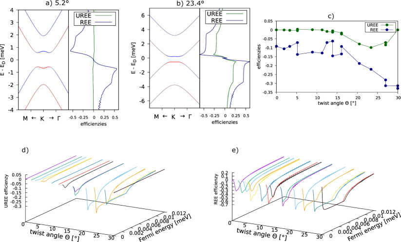
While we showed why there are only crossings (instead of anti-crossings) between the Dirac cone and any nearby NbSe2 bands, there is still the issue of distinguishing proximitized graphene transport properties from NbSe2 transport properties in experiments. For example, in a charge-to-spin conversion experiment, this distinction can be made by shifting the Fermi level by gating. A sign change of the signal, which is expected for the Dirac cone (see Fig. 5 a)), is a clear indicator that the signal is coming from the proximitized graphene rather than the NbSe2.
IV Proximity SOC
Fitting the low energy Dirac bands to the model Hamiltonian (see Eq. 3) gives the SOC parameters listed in Tab. 2 and shown in Fig. 4. As for other unrelaxed TMDC/graphene heterostructures (with semiconducting TMDCs, see Ref. Naimer et al. (2021)), the Kane-Mele SOC and the staggered potential are negligibly small. Starting at twist angle, both Rashba SOC () and valley-Zeeman SOC () have very similar size of about 0.5 meV to 1 meV. They stay at this level, until at starts to increase up to a value of meV at . Simultaneously decreases and vanishes at , which is a feature also seen in TMDC/graphene heterostructures with semiconducting TMDCs. Moreover, at roughly the same mark of , the Rashba phase angle increases as well, peaking at about with a value of . After this peak, rapidly decreases to at , which is demanded by symmetry.
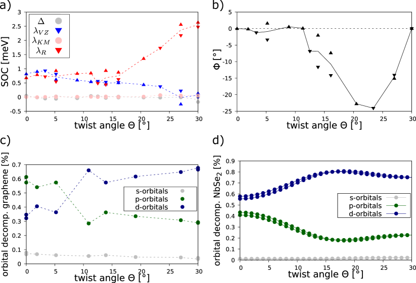
We argue that the main contribution of the proximity effect comes from the bands depicted in Fig. 2 d). This seems plausible since they are the energetically closest bands coupled to the Dirac cone through generalized Umklapp processes (see Ref. Koshino (2015)). Additionally, an orbital analysis shows that the orbital composition of these bands (Fig. 4 d)) compares well to the orbital composition of the NbSe2 orbitals found in the proximitized graphene’s Dirac cone (Fig. 4 c). Note that although both in Fig. 4 c) and Fig. 4 d) the twist-angle dependence is depicted, the data points in Fig. 4 c) come from the heterostructure calculations and the data points in Fig. 4 d) come from calculations of a NbSe2 monolayer along the black path depicted in Fig. 2 c). The twist-angle dependence takes the following form in both cases: While s-orbital contribution is negligible, p- and d-orbitals contribute similarly, with p-orbitals more dominant at twist angles near . There is one notable difference between the orbital composition of NbSe2 along the twist angle path and the orbital composition found in the actual heterostructures. Namely, that the ratio of p- and d-orbitals is slightly shifted in favour of the p-orbitals for the latter case for all twist angles. This can be attributed to the fact that the NbSe2 d-orbitals come exclusively from the Nb atoms and are therefore located farther away from the graphene.
Assuming these bands are responsible for the proximity SOC in the Dirac cone leads us to a plausible explanation for the twist-angle dependence seen in Fig. 4 a): For moderate strain (see black curve in Fig. 2 d)) the relevant contributing bands move towards the Dirac cone in energy, when going from to . At the same time, the splitting between the two spin-split subbands decreases and finally vanishes for . The general increase of the proximity SOC, while twisting from to can be seen as a consequence of the first point; if the contributing states are closer in energy, their influence and therefore the proximity SOC is expected to grow. Nevertheless, the decrease of the spin-splitting causes a decrease of the valley Zeeman SOC. This is to be expected, as the proximity valley-Zeeman SOC is mainly driven by a spin split in the NbSe2 substrate bands. However, this explanation is not complete, since it does not fully account for a possible change of orbital overlap between the Dirac cone and the NbSe2 bands. Especially, the large increase in Rashba SOC exceeds the expectation one might have from this simple picture. Also, the increase of the Rashba phase angle , which arises from a rather complex interference of phases, cannot be explained by such a handwaving argument. This underlines the need for the full DFT treatments, as done in this paper.
| [%] | [°] | [meV] | [meV] | [meV] | [meV] | [eV] | |
| 0.0 | 6.10 | 0 | 0.081 | -0.001 | -0.913 | 0.846 | -0.345 |
| 0.0 | 1.05 | 0 | 0.045 | 0.002 | 0.817 | 0.681 | -0.055 |
| 1.9 | 1.37 | 0 | -0.013 | -0.005 | 0.902 | 0.791 | -0.202 |
| 3.3 | -1.14 | -1 | -0.049 | 0.003 | 0.925 | 0.716 | -0.155 |
| 5.2 | -3.61 | -3 | 0.021 | 0.002 | 0.807 | 0.538 | -0.022 |
| 5.2 | 3.81 | 2 | -0.060 | 0.019 | 0.619 | 0.934 | -0.272 |
| 8.9 | 1.63 | 1 | -0.039 | 0.010 | 0.601 | 0.833 | -0.209 |
| 10.9 | -7.39 | -19 | -0.016 | 0.003 | 0.452 | 0.225 | 0.159 |
| 11.3 | 1.37 | 0 | 0.036 | 0.012 | 0.542 | 0.848 | -0.222 |
| 12.5 | -0.85 | -7 | 0.023 | 0.002 | 0.555 | 0.481 | 0.057 |
| 13.9 | -1.91 | -12 | -0.019 | 0.003 | 0.524 | 0.433 | 0.058 |
| 13.9 | 2.01 | -2 | -0.028 | 0.021 | 0.460 | 0.937 | -0.210 |
| 16.1 | 1.94 | -7 | 0.017 | 0.010 | 0.507 | 0.877 | -0.095 |
| 16.1 | -1.84 | -14 | -0.015 | 0.004 | 0.516 | 0.619 | -0.082 |
| 19.1 | 6.93 | -10 | -0.002 | 0.035 | -0.438 | 1.973 | -0.347 |
| 19.1 | -6.43 | -33 | 0.009 | 0.006 | 0.315 | 0.467 | 0.082 |
| 20.5 | -1.26 | -23 | -0.014 | 0.015 | 0.438 | 1.361 | -0.132 |
| 23.4 | -2.64 | -24 | -0.018 | 0.067 | 0.366 | 1.726 | -0.036 |
| 27.0 | -3.61 | -14 | -0.009 | 0.043 | 0.214 | 2.17 | 0.016 |
| 27.0 | 3.81 | -15 | 0.019 | 0.054 | -0.249 | 2.562 | -0.229 |
| 30.0 | -2.00 | 0 | 0.000 | 0.053 | 0.000 | 2.468 | -0.035 |
| 30.0 | 2.09 | 0 | -0.173 | 0.052 | 0.134 | 2.638 | -0.179 |
V Charge-to-spin conversion efficiencies
The Rashba SOC (and the resulting in-plane spin structure) in graphene based heterostructures enables the Rashba Edelstein effect Ghiasi et al. (2017); Offidani et al. (2017); Dyrdał et al. (2014); Edelstein (1990) (REE) and unconventional Rashba Edelstein effect Ingla-Aynés et al. (2022); Péterfalvi et al. (2022); Veneri et al. (2022); Lee et al. (2022); Camosi et al. (2022); Ontoso et al. (2023); Yang et al. (2023) (UREE) as efficient ways for charge-to-spin conversion. In the REE, the accumulated spins are perpendicular to the charge current, while they are collinear to it in the UREE. We analyze the potential of graphene proximitized by NbSe2 for this kind of charge-to-spin conversion. By using the Kubo formula Kubo (1956, 1957) in the Smrcka-Streda Smrcka and Streda (1977); Crépieux and Bruno (2001); Bonbien and Manchon (2020) formulation, we calculate the REE and UREE.
We assume weak disorder scattering describe by phenomenological parameter Freimuth et al. (2014); Železný et al. (2017); Bonbien and Manchon (2020); Lee et al. (2022). The change in the observable is given by
| (15) |
with the electric field strength and Fermi sea and Fermi surface susceptibilities and . Writing the formula in this form assumes that the electric field points only in one direction (in our case -direction). In a more general form the susceptibilities need an additional index, effectively forming a susceptibility tensor.
The integral is performed around and points ensuring to cover all the relevant states (151151 square grid with a side length of ). The integrands and are given by:
| (16) |
and
| (17) |
Here, and are the eigenenergy and eigenstate of band as represented by the model Hamiltonian Eq. (3) at . We set the broadening of the states to meV and the electronic temperature of the Fermi functions to meV. In our setup, the perturbation is always given by an electric field in the -direction, hence we used in the second matrix element for and . The physical observables are either for spin accumulation in - or -direction, with
| (18) |
or for the charge density response, with
| (19) |
As in Ref. Lee et al. (2022), we calculate the efficiency of the REE (or UREE) as the spin-y (or spin-x) accumulation normalized by the charge density response, so:
| (20) |
Fig. 5 a) and b) show the Fermi-energy dependent charge-to-spin efficiencies (REE and UREE) for two twist angles. Since for both cases Rashba SOC is dominating, the pattern (in accordance with Ref. Lee et al. (2022)) is the following: First, we note that as reported by other groups Lee et al. (2022); Dyrdał et al. (2014) both REE and UREE are anti-symmetric with respect to the Fermi level position. This means, that if the Fermi level lies in the Dirac cone valence bands, the sign of the charge-to-spin conversion is opposite compared to the case where the Fermi level lies in the conduction bands (see Fig. 5 a) and b)). Hence, the charge-to-spin conversion in the middle of the small band gap is zero. However, as soon as the Fermi level coincides with one of the inner bands, there is a peak in the charge-to-spin conversion. After this initial peak the efficiencies plateau, only to decrease again after the Fermi level touches the second band. The reason for the initial peak is the flatness of the bands at this energy, which comes from the presence of the valley-Zeeman SOC. In the plateau region the slope of the bands is constant and although increase (with increasing radius of the relevant contributing band), since increases at the same rate, the total charge-to-spin efficiencies stay constant. As soon as the second band starts contributing, the total efficiencies decay, because contributions from the two bands are of opposite sign. From this point on, the finite difference in contribution from the two bands stops the growth of . Therefore the charge-to-spin conversion vanishes in the limit of , since keeps increasing. This pattern is the same for both REE and UREE. While a) presents a case where the Rashba phase angle is very small, b) shows a case where . Therefore there is almost no sign of UREE in a), while in b) UREE and REE are comparable in size.
Fig. 5 d) and e) show UREE and REE respectively for all different investigated angles with strains . From these plots, one can already see the two main observations:
-
1.
UREE peaks at , the same twist angle that peaks at. This is very natural, since enables the radial in-plane spin structure and therefore UREE.
-
2.
Although the maximum value for the REE does not change drastically throughout all twist angles, the length of the plateau between the two conduction bands grows after and is largest at . This will lead to larger charge-to-spin yields, since in experiment the Fermi level cannot be fine tuned with the precision needed to exactly meet the peak.
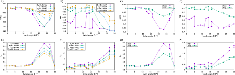
We visualize both points by plotting the (U)REE efficiencies averaged over 12 meV ( to meV) in Fig. 5 c). Using the peak efficiency instead of the average efficiency will give different results. We show those along with the results of an alternative (U)REE calculation (using Ref. Veneri et al. (2022)) in App. C.
VI Summary
We performed DFT calculations on several twisted graphene/NbSe2 supercells and extracted SOC parameters using a model Hamiltonian. Based on those fittings we additionally performed Kubo formula calculations giving us spin responses to an electric field and therefore (collinear and perpendicular) charge-to-spin conversion efficiencies. Since the heterostructure supercells have different twist angles , we can establish a twist-angle dependence for all SOC parameters and charge-to-spin conversion efficiencies. We find Rashba SOC to increase by a factor of 3 going from to . Furthermore, the Rashba phase angle peaks at . Consequently the perpendicular (REE) and collinear (UREE) charge-to-spin conversion efficiencies are also maximal at and respectively.
Additional investigations on the effect of external electric field and relaxation were performed on sample heterostructures. They indicate that the main effect of the electric field is an increase of the Rashba phase angle , while the main effect of relaxation is the change of interlayer distance and the resulting increase in general SOC strength. The typical rearrangement (linked to a CDW state) is observed, but does not change the proximity SOC significantly.
Acknowledgements.
All authors acknowledge support by the FLAG ERA JTC 2021 project 2DSOTECH. T. N. and J. F. were also supported by the European Union Horizon 2020 Research and Innovation Program 881603 (Graphene Flagship). M.G. acknowledges additional financial support provided by the Slovak Research and Development Agency provided under Contract No. APVV-SK-CZ-RD-21-0114 and Slovak Academy of Sciences project IMPULZ IM-2021-42.Appendix A Effects of electric field
The exact position of the Dirac cone with respect to the NbSe2 bands can have a very relevant influence on the proximity SOC. In order to study the band offset effect (as defined in Sec. III), we apply a transverse electrical field. The resulting SOC parameters are shown in Fig. 6 a) and c). While the Dirac cone is moved from very close vicinity to the NbSe2 bands ( eV) to well within the band gap ( eV), the Rashba SOC and valley-Zeeman SOC are decaying slightly. This decay seems to be rather weak since the lower bound for the band offset is almost zero (Dirac cone nearly touching the NbSe2 states). However, this is more understandable considering that those very close NbSe2 states do not interact with the Dirac cone. The nearest states actually interacting with the Dirac cone are 800 meV lower in energy. Contrary to the rather small change of and , the Rashba phase angle nearly doubles in magnitude, while the Dirac cone is being shifted further into the band gap. Fig. 6 b) shows which NbSe2 bands contribute to the Dirac cone. Except for a slight shift towards -orbitals, the orbital composition stays roughly constant.
Appendix B Effects of relaxation
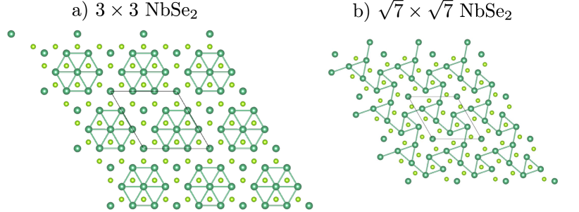
All results in the main paper are concerned with idealized structures with a fixed interlayer distance and unrelaxed structures of both graphene and NbSe2. The results of Ref. Naimer et al. (2021) indicate that the relaxation of graphene/transition-metal dichalcogenide heterostructures has little direct effect on the proximity SOC. Instead it enhances the unwanted effects (such as an increase of the staggered potential ) of the strain necessary to construct the commensurate supercell. However, NbSe2 is known to exhibit a periodic lattice distortion with charge density wave for 3 supercells Ugeda et al. (2016); Xi et al. (2015); Lian et al. (2018), where the atoms rearrange in a triangular or possibly other Guster et al. (2019) structure. Since this might introduce relevant changes in electronic structure, we performed additional relaxation calculations on and larger heterostructures. The results of these relaxations are shown in Fig. 7, where we plot the most prevalent Nb-Nb bonds (bond lengths must be bigger than the unrelaxed Nb-Nb distance of 3.48 Å). By doing this, we show the rearrangement of the 3 supercell into filled hexagons. It is the same pattern, which arises, if we perform the relaxation calculations without the graphene layer. This shows that (at least regarding the rearrangement) the CDW phase is unchanged by the nearby layer of graphene. The other supercell for comparison shows another pattern, which is most likely caused by the nearby graphene layer. Its maximal difference in Nb-Nb bond length is much smaller (about mÅ) than the one of the supercell (about mÅ).
Naturally, the question arises: Does this rearranging change the proximity SOC in either of the two heterostructures? For both heterostructures and decrease by about 35% (see Tab. 3). However, this can be attributed to the change of the interlayer distance between graphene and NbSe2, which we apparently slightly underestimated in the calculations of the main paper. The equilibrium interlayer distance as determined by the relaxation calculations is about 3.5% larger than the one we assumed. According to the interlayer distance study presented in Ref. Gmitra et al. (2016) the decrease in SOC is roughly what can be expected for such an increased interlayer distance. Additionally, as expected, through the relaxation there is an increase in the parameters and , which are suppressed in the idealized structures. Based on our limited relaxation calculations, we estimate that the formation of the rearranged triangular pattern typical for CDW can largely be considered not relevant for the proximity SOC effects.
| relaxed | |||||||||
|---|---|---|---|---|---|---|---|---|---|
| [∘] | [ | [∘] | [meV] | [meV] | [meV] | [meV] | |||
| (0,4) | (0,3) | 0.0 | 6.10 | no | 0 | 0.081 | -0.001 | -0.913 | 0.846 |
| (0,4) | (0,3) | 0.0 | 6.10 | yes | 0 | -0.649 | -0.018 | -0.559 | 0.571 |
| (3,1) | (2,1) | 5.2 | 3.81 | no | 2 | -0.060 | 0.019 | 0.619 | 0.934 |
| (3,1) | (2,1) | 5.2 | 3.81 | yes | 2 | 0.491 | -0.091 | 0.409 | 0.604 |
Appendix C Details of Charge-to-spin calculations
In Sec. V we calculated efficiencies for the Rashba Edelstein effect (REE) and the unconventional Rashba Edelstein effect (UREE) using a Kubo formula approach. Since these efficiencies depend on both the twist angle and the Fermi energy, we plotted the data in a fenceplot (see Fig. 5 d) and e)). Here, we present alternative presentation forms. Fig. 8 a) and b) show the data as cuts of different Fermi levels through the fence plot data. In Fig. 8 c) and d) we plot two different measures for the total (U)REE (more precise: the value with maximal absolute value) of the (U)REE and the value averaged over 12 meV ( to meV). The latter is the same as shown in Fig. 5 c). For the UREE (Fig. 8 c)) both measures convey the same message, since the total value is far from being capped by the maximally possible value. Taking into account only Rashba SOC, which is the source of both UREE and REE, this maximally possible value is . Other terms like can bend the band structure in a way that flat bands give rise to a local maximum surpassing a certain Fermi level, while diminishing it for other Fermi levels. This can give a distorted picture of the truth, since in reality, fine tuning the Fermi level this precise might be impossible. Hence, for the REE (Fig. 8 d)), the averaged curve gives a better overall picture of the true physics, as realizing an efficient REE device is easier with the broad high plateau of the 30∘ case. The drawback of plotting the averaged efficiency is that a range has to be specified over which the average has been taken. We assume that at meV the (U)REE has decayed enough and no new physics will emerge. Therefore this is the measure we use in the main paper.
We additionally use a different formula, which was given in Ref. Veneri et al. (2022), to calculate a measure for the charge-to-spin response of the system. It is derived within linear response theory as well and has an easy analytical form. It takes the same parameters, i.e. the parameters of the model Hamiltonian plus the Fermi level. The resulting quantities and can broadly be compared to the charge-to-spin conversion efficiencies ( and ) we calculate. However, they are not normalized by the charge density responses. The figure of merit given in Ref. Veneri et al. (2022) is more adequate to compare to and also has the correct sign. But since this would require information about the charge density response, we opt to use and instead. By showing the results in arbitrary units, we avoid the problem of having to give estimates for the other parameters of their model, which represent impurity strength and impurity density. Since we only want to compare the values of different twist angle, we deem this approach valid. We use the same set of parameters (determined by our fittings) as we used for the numerical approach. The results are shown in Fig. 8 e)-h). Because the analytical formula is only valid for a Fermi level, where both subbands are already occupied, we change the range of Fermi levels to fulfil this condition for all twist angles (6 meV meV). For our set of parameter data we can conclude that both models qualitatively give the same intuitive results. However, there are two differences we can see:
-
1.
the analytical formula estimates the peak of the UREE to be slightly (about 3∘) to the right of the one determined by our numerical approach.
-
2.
the overall twist-angle tuneability is enhanced compared to the predictions of the numerical approach.
References
- Geim and Grigorieva (2013) A. K. Geim and I. V. Grigorieva, “Van der Waals heterostructures,” Nature 499, 419 (2013).
- Duong et al. (2017) Dinh Loc Duong, Seok Joon Yun, and Young Hee Lee, “Van der Waals Layered Materials: Opportunities and Challenges,” ACS Nano 11, 11803 (2017).
- Bolotin et al. (2008) K.I. Bolotin, K.J. Sikes, Z. Jiang, M. Klima, G. Fudenberg, J. Hone, P. Kim, and H.L. Stormer, “Ultrahigh electron mobility in suspended graphene,” Solid State Communications 146, 351–355 (2008).
- Du et al. (2008) Xu Du, Ivan Skachko, Anthony Barker, and Eva Y. Andrei, “Approaching ballistic transport in suspended graphene,” Nature Nanotechnology 3, 491–495 (2008).
- Singh et al. (2016) Simranjeet Singh, Jyoti Katoch, Jinsong Xu, Cheng Tan, Tiancong Zhu, Walid Amamou, James Hone, and Roland Kawakami, “Nanosecond spin relaxation times in single layer graphene spin valves with hexagonal boron nitride tunnel barriers,” Appl. Phys. Lett. 109, 122411 (2016).
- Drögeler et al. (2016) Marc Drögeler, Christopher Franzen, Frank Volmer, Tobias Pohlmann, Luca Banszerus, Maik Wolter, Kenji Watanabe, Takashi Taniguchi, Christoph Stampfer, and Bernd Beschoten, “Spin Lifetimes Exceeding 12 ns in Graphene Nonlocal Spin Valve Devices,” Nano Lett. 16, 3533 (2016).
- Gmitra and Fabian (2015) Martin Gmitra and Jaroslav Fabian, “Graphene on transition-metal dichalcogenides: A platform for proximity spin-orbit physics and optospintronics,” Phys. Rev. B 92, 155403 (2015).
- Gmitra et al. (2016) Martin Gmitra, Denis Kochan, Petra Högl, and Jaroslav Fabian, “Trivial and inverted dirac bands and the emergence of quantum spin hall states in graphene on transition-metal dichalcogenides,” Phys. Rev. B 93, 155104 (2016).
- Wang et al. (2015a) Zhe Wang, Dong-Keun Ki, Hua Chen, Helmuth Berger, Allan H MacDonald, and Alberto F Morpurgo, “Strong interface-induced spin-orbit interaction in graphene on WS2,” Nat. Commun. 6, 8339 (2015a).
- Avsar et al. (2014) A Avsar, J Y Tan, T Taychatanapat, J Balakrishnan, G. K. W. Koon, Y Yeo, J Lahiri, A Carvalho, A S Rodin, E. C. T. O’Farrell, G Eda, A H Castro Neto, and B. Özyilmaz, “Spin–orbit proximity effect in graphene,” Nat. Commun. 5, 4875 (2014).
- Naimer et al. (2021) Thomas Naimer, Klaus Zollner, Martin Gmitra, and Jaroslav Fabian, “Twist-angle dependent proximity induced spin-orbit coupling in graphene/transition metal dichalcogenide heterostructures,” Phys. Rev. B 104, 195156 (2021).
- Naimer and Fabian (2023) Thomas Naimer and Jaroslav Fabian, “Twist-angle dependent proximity induced spin-orbit coupling in graphene/topological insulator heterostructures,” Phys. Rev. B 107, 195144 (2023).
- Zollner et al. (2023) Klaus Zollner, Simão M. João, Branislav K. Nikolić, and Jaroslav Fabian, “Twist- and gate-tunable proximity spin-orbit coupling, spin relaxation anisotropy, and charge-to-spin conversion in heterostructures of graphene and transition metal dichalcogenides,” Phys. Rev. B 108, 235166 (2023).
- Karpiak et al. (2019) Bogdan Karpiak, Aron W Cummings, Klaus Zollner, Marc Vila, Dmitrii Khokhriakov, Anamul Md Hoque, André Dankert, Peter Svedlindh, Jaroslav Fabian, Stephan Roche, and Saroj P Dash, “Magnetic proximity in a van der waals heterostructure of magnetic insulator and graphene,” 2D Materials 7, 015026 (2019).
- Wang et al. (2015b) Zhiyong Wang, Chi Tang, Raymond Sachs, Yafis Barlas, and Jing Shi, “Proximity-induced ferromagnetism in graphene revealed by the anomalous hall effect,” Phys. Rev. Lett. 114, 016603 (2015b).
- Wei et al. (2016) Peng Wei, Sunwoo Lee, Florian Lemaitre, Lucas Pinel, Davide Cutaia, Wujoon Cha, Ferhat Katmis, Yu Zhu, Donald Heiman, James Hone, Jagadeesh S. Moodera, and Ching-Tzu Chen, “Strong interfacial exchange field in the graphene/EuS heterostructure,” Nat. Mater. 15, 711 (2016).
- Zhang et al. (2015) Jiayong Zhang, Bao Zhao, Yugui Yao, and Zhongqin Yang, “Robust quantum anomalous hall effect in graphene-based van der waals heterostructures,” Phys. Rev. B 92, 165418 (2015).
- Zollner et al. (2018) Klaus Zollner, Martin Gmitra, and Jaroslav Fabian, “Electrically tunable exchange splitting in bilayer graphene on monolayer Cr 2 X 2 Te 6 with X = Ge, Si, and Sn,” New J. Phys. 20, 073007 (2018).
- Zhang et al. (2018) Jiayong Zhang, Bao Zhao, Tong Zhou, Yang Xue, Chunlan Ma, and Zhongqin Yang, “Strong magnetization and Chern insulators in compressed graphene/CrI3 van der Waals heterostructures,” Phys. Rev. B 97, 085401 (2018).
- Gani et al. (2019) Yohanes S. Gani, Hadar Steinberg, and Enrico Rossi, “Superconductivity in twisted graphene heterostructures,” Phys. Rev. B 99, 235404 (2019).
- Moriya et al. (2020) Rai Moriya, Naoto Yabuki, and Tomoki Machida, “Superconducting proximity effect in a van der waals junction,” Phys. Rev. B 101, 054503 (2020).
- Zhang et al. (2020) Zhiming Zhang, Kenji Watanabe, Takashi Taniguchi, and Brian J. LeRoy, “Local characterization and engineering of proximitized correlated states in vertical heterostructures,” Phys. Rev. B 102, 085429 (2020).
- Wang et al. (2017) Hong Wang, Xiangwei Huang, Junhao Lin, Jian Cui, Yu Chen, Chao Zhu, Fucai Liu, Qingsheng Zeng, Jiadong Zhou, Peng Yu, Xuewen Wang, Haiyong He, Siu Hon Tsang, Weibo Gao, Kazu Suenaga, Fengcai Ma, Changli Yang, Li Lu, Ting Yu, Edwin Hang Tong Teo, Guangtong Liu, and Zheng Liu, “High-quality monolayer superconductor nbse2 grown by chemical vapour deposition,” Nature Communications 8, 394 (2017).
- Xi et al. (2016) Xiaoxiang Xi, Zefang Wang, Weiwei Zhao, Ju-Hyun Park, Kam Tuen Law, Helmuth Berger, László Forró, Jie Shan, and Kin Fai Mak, “Ising pairing in superconducting nbse2 atomic layers,” Nature Physics 12, 139–143 (2016).
- Khestanova et al. (2018) E. Khestanova, J. Birkbeck, M. Zhu, Y. Cao, G. L. Yu, D. Ghazaryan, J. Yin, H. Berger, L. Forró, T. Taniguchi, K. Watanabe, R. V. Gorbachev, A. Mishchenko, A. K. Geim, and I. V. Grigorieva, “Unusual suppression of the superconducting energy gap and critical temperature in atomically thin nbse2,” Nano Letters 18, 2623–2629 (2018), pMID: 29529377, https://doi.org/10.1021/acs.nanolett.8b00443 .
- Li and Koshino (2019) Yang Li and Mikito Koshino, “Twist-angle dependence of the proximity spin-orbit coupling in graphene on transition-metal dichalcogenides,” Phys. Rev. B 99, 075438 (2019).
- David et al. (2019) Alessandro David, Péter Rakyta, Andor Kormányos, and Guido Burkard, “Induced spin-orbit coupling in twisted graphene–transition metal dichalcogenide heterobilayers: Twistronics meets spintronics,” Phys. Rev. B 100, 085412 (2019).
- Péterfalvi et al. (2022) Csaba G. Péterfalvi, Alessandro David, Péter Rakyta, Guido Burkard, and Andor Kormányos, “Quantum interference tuning of spin-orbit coupling in twisted van der waals trilayers,” Phys. Rev. Research 4, L022049 (2022).
- Lee et al. (2022) Seungjun Lee, D. J. P. de Sousa, Young-Kyun Kwon, Fernando de Juan, Zhendong Chi, Fèlix Casanova, and Tony Low, “Charge-to-spin conversion in twisted heterostructures,” Phys. Rev. B 106, 165420 (2022).
- Yang et al. (2023) Haozhe Yang, Beatriz Martín-García, Jozef Kimák, Eva Schmoranzerová, Eoin Dolan, Zhendong Chi, Marco Gobbi, Petr Němec, Luis E. Hueso, and Fèlix Casanova, “Twist-angle tunable spin texture in wse2/graphene van der waals heterostructures,” (2023), arXiv:2312.10227 [cond-mat.mes-hall] .
- Ingla-Aynés et al. (2022) Josep Ingla-Aynés, Inge Groen, Franz Herling, Nerea Ontoso, C K Safeer, Fernando de Juan, Luis E Hueso, Marco Gobbi, and Fèlix Casanova, “Omnidirectional spin-to-charge conversion in graphene/NbSe2 van der waals heterostructures,” 2D Materials 9, 045001 (2022).
- Veneri et al. (2022) Alessandro Veneri, David T. S. Perkins, Csaba G. Péterfalvi, and Aires Ferreira, “Twist angle controlled collinear edelstein effect in van der waals heterostructures,” Phys. Rev. B 106, L081406 (2022).
- Camosi et al. (2022) Lorenzo Camosi, Josef Světlík, Marius V Costache, Williams Savero Torres, Iván Fernández Aguirre, Vera Marinova, Dimitre Dimitrov, Marin Gospodinov, Juan F Sierra, and Sergio O Valenzuela, “Resolving spin currents and spin densities generated by charge-spin interconversion in systems with reduced crystal symmetry,” 2D Materials 9, 035014 (2022).
- Ontoso et al. (2023) Nerea Ontoso, C. K. Safeer, Franz Herling, Josep Ingla-Aynés, Haozhe Yang, Zhendong Chi, Beatriz Martin-Garcia, Iñigo Robredo, Maia G. Vergniory, Fernando de Juan, M. Reyes Calvo, Luis E. Hueso, and Fèlix Casanova, “Unconventional charge-to-spin conversion in graphene/ van der waals heterostructures,” Phys. Rev. Appl. 19, 014053 (2023).
- Ghiasi et al. (2017) Talieh S. Ghiasi, Josep Ingla-Aynés, Alexey A. Kaverzin, and Bart J. Van Wees, “Large Proximity-Induced Spin Lifetime Anisotropy in Transition-Metal Dichalcogenide/Graphene Heterostructures,” Nano Lett. 17, 7528 (2017).
- Offidani et al. (2017) Manuel Offidani, Mirco Milletari, Roberto Raimondi, and Aires Ferreira, “Optimal charge-to-spin conversion in graphene on transition-metal dichalcogenides,” Phys. Rev. Lett. 119, 196801 (2017).
- Dyrdał et al. (2014) A. Dyrdał, J. Barnaś, and V. K. Dugaev, “Current-induced spin polarization in graphene due to rashba spin-orbit interaction,” Phys. Rev. B 89, 075422 (2014).
- Edelstein (1990) V.M. Edelstein, “Spin polarization of conduction electrons induced by electric current in two-dimensional asymmetric electron systems,” Solid State Communications 73, 233–235 (1990).
- Kiemle et al. (2022) Jonas Kiemle, Lukas Powalla, Katharina Polyudov, Lovish Gulati, Maanwinder Singh, Alexander W. Holleitner, Marko Burghard, and Christoph Kastl, “Gate-tunable helical currents in commensurate topological insulator/graphene heterostructures,” ACS Nano 16, 12338–12344 (2022), pMID: 35968692, https://doi.org/10.1021/acsnano.2c03370 .
- Zhang et al. (2014) Junhua Zhang, C. Triola, and E. Rossi, “Proximity effect in graphene–topological-insulator heterostructures,” Phys. Rev. Lett. 112, 096802 (2014).
- Song et al. (2018) Kenan Song, David Soriano, Aron W. Cummings, Roberto Robles, Pablo Ordejón, and Stephan Roche, “Spin Proximity Effects in Graphene/Topological Insulator Heterostructures,” Nano Lett. 18, 2033 (2018).
- Ding et al. (2011) Yi Ding, Yanli Wang, Jun Ni, Lin Shi, Siqi Shi, and Weihua Tang, “First principles study of structural, vibrational and electronic properties of graphene-like mx2 (m=mo, nb, w, ta; x=s, se, te) monolayers,” Physica B: Condensed Matter 406, 2254–2260 (2011).
- Koda et al. (2016) Daniel S Koda, Friedhelm Bechstedt, Marcelo Marques, and Lara K Teles, “Coincidence lattices of 2d crystals: heterostructure predictions and applications,” The Journal of Physical Chemistry C 120, 10895–10908 (2016).
- Carr et al. (2020) Stephen Carr, Shiang Fang, and Efthimios Kaxiras, “Electronic-structure methods for twisted moiré layers,” Nature Reviews Materials 5, 748–763 (2020).
- Hohenberg and Kohn (1964) P. Hohenberg and W. Kohn, “Inhomogeneous electron gas,” Phys. Rev. 136, B864 (1964).
- Giannozzi and et al. (2009) Paolo Giannozzi and et al., “Quantum espresso: a modular and open-source software project for quantum simulations of materials,” J. Phys.: Cond. Mat. 21, 395502 (2009).
- Kane and Mele (2005) C. L. Kane and E. J. Mele, “Quantum Spin hall effect in graphene,” Phys. Rev. Lett. 95, 226801 (2005).
- Ugeda et al. (2016) Miguel M. Ugeda, Aaron J. Bradley, Yi Zhang, Seita Onishi, Yi Chen, Wei Ruan, Claudia Ojeda-Aristizabal, Hyejin Ryu, Mark T. Edmonds, Hsin-Zon Tsai, Alexander Riss, Sung-Kwan Mo, Dunghai Lee, Alex Zettl, Zahid Hussain, Zhi-Xun Shen, and Michael F. Crommie, “Characterization of collective ground states in single-layer nbse2,” Nature Physics 12, 92–97 (2016).
- Xi et al. (2015) Xiaoxiang Xi, Liang Zhao, Zefang Wang, Helmuth Berger, László Forró, Jie Shan, and Kin Fai Mak, “Strongly enhanced charge-density-wave order in monolayer nbse2,” Nature Nanotechnology 10, 765–769 (2015).
- Lian et al. (2018) Chao-Sheng Lian, Chen Si, and Wenhui Duan, “Unveiling charge-density wave, superconductivity, and their competitive nature in two-dimensional nbse2,” Nano Letters 18, 2924–2929 (2018).
- Koshino (2015) Mikito Koshino, “Interlayer interaction in general incommensurate atomic layers,” New Journal of Physics 17, 015014 (2015).
- Kubo (1956) R. Kubo, “A general expression for the conductivity tensor,” Canadian Journal of Physics 34, 1274–1277 (1956), https://doi.org/10.1139/p56-140 .
- Kubo (1957) Ryogo Kubo, “Statistical-mechanical theory of irreversible processes. i. general theory and simple applications to magnetic and conduction problems,” Journal of the Physical Society of Japan 12, 570–586 (1957), https://doi.org/10.1143/JPSJ.12.570 .
- Smrcka and Streda (1977) L Smrcka and P Streda, “Transport coefficients in strong magnetic fields,” Journal of Physics C: Solid State Physics 10, 2153 (1977).
- Crépieux and Bruno (2001) A. Crépieux and P. Bruno, “Theory of the anomalous hall effect from the kubo formula and the dirac equation,” Phys. Rev. B 64, 014416 (2001).
- Bonbien and Manchon (2020) Varga Bonbien and Aurélien Manchon, “Symmetrized decomposition of the kubo-bastin formula,” Phys. Rev. B 102, 085113 (2020).
- Freimuth et al. (2014) Frank Freimuth, Stefan Blügel, and Yuriy Mokrousov, “Spin-orbit torques in co/pt(111) and mn/w(001) magnetic bilayers from first principles,” Phys. Rev. B 90, 174423 (2014).
- Železný et al. (2017) Jakub Železný, Yang Zhang, Claudia Felser, and Binghai Yan, “Spin-polarized current in noncollinear antiferromagnets,” Phys. Rev. Lett. 119, 187204 (2017).
- Guster et al. (2019) Bogdan Guster, Carmen Rubio-Verdú, Roberto Robles, Javier Zaldívar, Paul Dreher, Miguel Pruneda, José Ángel Silva-Guillén, Deung-Jang Choi, José I. Pascual, Miguel M. Ugeda, Pablo Ordejón, and Enric Canadell, “Coexistence of elastic modulations in the charge density wave state of 2h-nbse2,” Nano Letters 19, 3027–3032 (2019).