Fermi arcs mediated transport in inversion symmetry-broken Weyl semimetal nanowire and its hybrid junctions
Abstract
The emergence of gapless surface states, known as Fermi arcs (FAs), is one of the unique properties of the novel topological Weyl semimetal (WSM). However, extracting the signatures of FAs from the bulk states has always been a challenge as both of them are gapless in nature and connected to each other. We capture the signatures of FAs via transport in an inversion symmetry (IS)-broken WSM. We study the band structure and the properties of FAs like shape, spin polarization considering slab and nanowire (NW) geometry, and then compute the two-terminal conductance in WSM NW in terms of the scattering coefficients within the Landauer formalism. We find the FA-mediated conductance to be quantized in units of . We extend our study to the transport in WSM/Weyl superconductor (WSC) NW hybrid junction using the Blonder-Tinkham-Klapwijk (BTK) formalism. We show that due to the intricate spin textures, the signatures of the FAs can be captured via Andreev reflection process. We also show that our results of conductance are robust against delta-correlated quenched disorder and thus enhancing the experimental feasibility.
I Introduction
Over the past decade, Weyl semimetal (WSM) has emerged as a novel gapless topological phase in three dimensional (D) semimetals due to its nontrivial band structure and intriguing transport properties Armitage et al. (2018); Rao (2016); McCormick et al. (2017); Yan and Felser (2017); Burkov (2018). Weyl fermions were initially proposed as a solution of massless Dirac equation in 1929 Dirac and Fowler (1928); Weyl (1929). Later, these fermions as low energy excitations, have been theoretically proposed in D topological insulators at the transition phase between the trivial and nontrivial insulating phases by breaking either time reversal symmetry (TRS) or inversion symmetry (IS) Murakami (2007); Vazifeh and Franz (2013), topological insulator heterostructures Burkov and Balents (2011); Burkov et al. (2011); Zyuzin et al. (2012); Zyuzin and Burkov (2012); Halász and Balents (2012); Liu et al. (2013), pyrochlore iridates Wan et al. (2011); Bzdušek et al. (2015); Witczak-Krempa and Kim (2012) etc. The experimental realizations of WSM phase in real materials e.g., TaAs, TaP, NbAs, NbP, WTe2, magnetic Heusler materials etc. Lv et al. (2015a, b, c); Lu et al. (2015); Xu et al. (2015a, b, c); Soluyanov et al. (2015); Moll et al. (2016); Wang et al. (2016a); Xu et al. (2015d); Ojanen (2013); Sun et al. (2015a); Feng et al. (2016); Xu et al. (2016); Potter et al. (2014); Xu et al. (2015d, 2016) have opened up the opportunity for the plethora of research works for both theorists and experimentalists.
WSMs exhibit a unique bulk band structure where the valence and conduction bands intersect at an even number (minimum two for TRS-broken and four for IS-broken WSM) of isolated points in momentum space known as Weyl nodes (WNs). Around these WNs, the bulk bands disperse linearly with momentum, resembling the dispersion of D massless relativistic fermions. WNs are recognized as the monopoles of Berry curvature in momentum space, while their charge, termed chirality, determines their topological nature Armitage et al. (2018); Rao (2016); McCormick et al. (2017); Yan and Felser (2017); Burkov (2018). Importantly, WNs always apear pairwise with opposite chiralities, ensuring a net zero chiral charge over the entire Brillouin zone. Effects of both weak and strong disorder Altland and Bagrets (2016); Shapourian and Hughes (2016); Klier et al. (2019); Sbierski et al. (2014); Chen et al. (2015), and interactions Maciejko and Nandkishore (2014); Witczak-Krempa et al. (2014); Hosseini and Askari (2015); Jacobs et al. (2016); Laubach et al. (2016); Roy et al. (2017); Boettcher (2020) on the WSM phase have been investigated.
In addition to the nontrivial bulk bands, an intriguing and exotic aspect of WSMs is the presence of nontrivial surface states, known as Fermi arcs (FAs) Lv et al. (2015a, b, c); Moll et al. (2016); Xu et al. (2015c, a, b, 2011); Sun et al. (2015b, c); Wang et al. (2018); Chen et al. (2020); Li et al. (2015). When projected onto a surface Brillouin zone (sBZ), these surface states manifest as arcs with their endpoints located at the projection of the bulk WNs on the sBZ. Close to the projection of the WNs, FAs states can leak into the bulk and reappear at the opposite sBZ Armitage et al. (2018); Rao (2016); McCormick et al. (2017). Notably, both surface and bulk states of WSMs are gapless. This is in sharp contrast to the D topological insulators, where gapless surface states lie within the bulk gap and are exponentially localized near the surface. Signatures of these FAs in transport properties have been investigated both theoretically Baireuther et al. (2016); Gorbar et al. (2016); Igarashi and Koshino (2017); Breitkreiz and Brouwer (2019); Mukherjee et al. (2018); Kaladzhyan and Bardarson (2019) and experimentally Li et al. (2015); Wang et al. (2016a, 2018); Chen et al. (2020).
Due to the gaplessness nature, separating these surface states from the bulk and identifying the sole signatures of FAs in the transport measurement has always been a challenging task. Very recently, it has been shown that bulk states are gapped out in TRS-broken WSM nanowire (NW) due to its finite size effect. Within the bulk confinement gap, only surface states are present and their contributions to the conductance becomes quantized in units of in a two-terminal setup Kaladzhyan and Bardarson (2019). However, most of the WSM phases in reality are observed to be ISB because of the plenty of crystal structure asymmetries found in nature.
In recent years, investigation of transport properties in superconducting hybrid junctions of WSMs have attracted significant attention due to the interplay of superconductivity and the non-trivial topology of WSMs Meng and Balents (2012); Cho et al. (2012); Uchida et al. (2014); Khanna et al. (2016); Mukherjee et al. (2017); Zhang et al. (2018a, b); Saxena et al. (2023); Dutta et al. (2020); Saxena et al. (2023); Chatterjee and Dutta . Most of these studies concern the bulk properties of WSM. Transport phenomena become much more subtle and fascinating when the role of surface states are also taken into account Khanna et al. (2014); Bednik et al. (2015); Chen and Franz (2016); Baireuther et al. (2017); Dutta and Black-Schaffer (2019); Faraei and Jafari (2019); Zheng et al. (2021). Till date, there are a few studies on FA mediated transport phenomena exist in the literature Baum et al. (2015); Kaladzhyan and Bardarson (2019); Pareek and Kundu ; Kumari et al. ; Kuibarov et al. (2024). Particularly, signatures of FAs in IS broken (ISB) Weyl NW hybrid junctions have not been investigated so far in the literature, to the best of our knowledge. Since NW junctions are very useful in separating the contributions due to FAs, it remains interesting to look for the role of FAs in transport phenomena via the Andreev reflection (AR) in Weyl NW-based superconducting hybrid junctions.
With these motivations, in this present article, we investigate ISB WSM NW in a two-terminal set-up in two conditions: (i) bare NW and (ii) its hybrid junction with superconducting pairing (WSC) tailoring a WSM/WSC NW junction as shown in Fig. 1. Here, superconductivity in WSC NW can be generated either via the proximity effect Khanna et al. (2014) or electron-electron correlation Bednik et al. (2015); Sekine and Nomura (2013); Qin et al. (2019); Cho et al. (2012). In our work, we address the following intriguing questions: Is it possible to separate out the contributions of FAs from the bulk states in ISB WSM NW, similar to the TRS-broken WSM case? Is it possible to capture the signature of FAs via the Andreev process in such hybrid junction? Does the transport signature become quantized in ISB WSM junctions too? Are these quantizations robust against disorder?
The rest of the article is organized as follows. In Sec. II, we introduce our model, compute and analyse the band structure and FAs in slab and NW geometry. In Sec. III, we investigate the conductance in WSM NW and WSM/WSC NW hybrid juction, and subsequently in Sec. IV, we check the robustness of our results against the random onsite disorder. Finally, in Sec. V, we summarize and conclude our results.
II Model and Band Structure
In this section, we first introduce our model of ISB WSM and WSM with superconducting correlation. For the discussion on the WSM phase in detail, we show the bulk band structure, followed by a thorough discussions on the surface states. To obtain the surface states, we require finite boundary which can be achieved by making the WSM finite atleast along one direction.
For the sake of understanding the nature of surface states in detail, let us consider two different geometries: (i) slab where it is fintie along direction and (ii) NW where it is finite along both - and -directions. In the slab geometry, we depict the locations of the FAs with their spin-textures. For the NW geometry which is our main concern, we discuss the surface states in WSM and WSC phase, with both open boundary condition (OBC) and periodic boundary condition (PBC).
II.1 Model Hamiltonian
We consider an ISB WSM described by the second-quantized Hamiltonian on a cubic lattice with lattice spacing () given by,
| (1) |
where, and represents the annihilation (creation) operator for an electron in the orbital and spin . The momentum, (), run over the first BZ. Here, is described by the four band model as Kourtis et al. (2016); Zhang et al. (2018b); Saxena et al. (2023),
| (2) | |||||
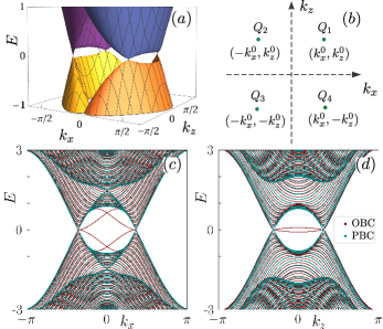
where, and represent the spin-orbit coupling and nearest-neighbour hopping amplitudes, respectively, is the crystal-field splitting energy, and are the real parameters of the model. The Pauli matrices and for act on the orbital and spin degrees of freedom of the electron, respectively. The term in Eq. (2) is responsible for the breaking of IS, whereas the TRS is preserved following the conditions: and where and , with being the complex conjugation operator. Broken IS leads to four WNs located at , with and as depicted in Fig. 2(a-b). The presence of TRS implies that the WNs must appear in Kramer pairs (KPs) Armitage et al. (2018); Rao (2016). In our model, and form these KPs. TRS also ensures that WNs within a KP share the same chirality. Consequently, the overall chirality of the system remains zero. Following that, the chiralities of are opposite to that of .
For the superconducting part of the Hamltonian, we consider -wave spin-singlet intra-orbital pairing which couples the electrons and holes between the WNs with same chirality i.e., between and Zhang et al. (2018b, a); Saxena et al. (2023). With this consideration, the Bogoliubov-de Gennes (BdG) Hamiltonian for the WSC part can be written as:
| (3) |
where,
| (4) |
with as the Nambu spinor. The Pauli matrices, , act on the particle-hole degree of freedom. Here, denotes the -wave pairing potential and is the chemical potential measured with respect to Weyl nodes. For the rest of the article, we choose the following parameter values in our model: , , , , , , and . Note that, the qualitative behavior of our results are not sensitive to the change in the parameter values as long as WSM phase is preserved.
II.2 Slab geometry
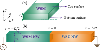
With the discussions on the bulk properties, we now focus on the surface FA states in WSM. For that, we consider a slab geometry schematically shown in Fig. 1(a). Since the WNs are located in the plane, we choose a slab to have a finite size along -direction with thickness such that the projection of all the four WNs can be observed in the sBZ. Along the -and -directions, the WSM slab is infinite, so the momenta along these directions are still good quantum numbers. Consideration of the finite size along the -direction gives rise to two surfaces located at (bottom surface) and (top surface) as shown Fig. 1().
Since the momentum along the -direction is not well defined, to find the band structure in slab geometry we first obtain the real space Hamiltonian by performing an inverse Fourier transformation (FT) only along the -direction using
| (5) |
With this transformation, the Hamiltonian takes the form,
where,
| (6) | |||||
We numerically diagonalize the above Hamiltonian for each set of values with slices considering both OBC and PBC along -direction. Note that, surface states can be observed only in OBC, while PBC is employed to identify only the bulk states. We show the band structure as a function of by setting in Fig. 2(c). The choice of can be made anywhere in between [] since the surface states only appear in between the WNs with opposite chiralities. Similarly, we depict the band structure as a function of with in Fig. 2(d) employing both OBC and PBC along -direction. In both the figures, we observe the gapless dispersive FA surface states between the WNs when OBC is implemented.
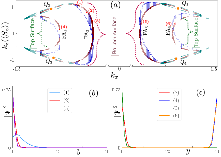
Now, we investigate the shape of the FAs obtained in the WSM slab geometry. FAs are the open constant energy contours in the plane residing at the boundary of the system. We fix the energy at ( sets the energy scale in the system) and draw the Fermi surface in Fig. 3(). With the OBC, we observe the existence of four FAs denoted by FAγ with . As expected, two FAs connect WNs with opposite chirality i.e., FA1 and FA2 (FA3 and FA4) connect the WNs, and ( and ). On top of FAs, we also show the Fermi surface in PBC, which only contains the bulk states around each WN as shown in Fig. 3() using teal color. Interestingly, the shape of FAs obtained in this model closely resembles the FAs observed in real materials Lv et al. (2015c); Xu et al. (2016); Sun et al. (2015a); Xu et al. (2015a, c); Lv et al. (2015b).
To get insight about the locations of the states on the FAs in the real space, we depict () as a function of in Fig. 3(b-c) for the states on the FAs marked in red dots [see Fig. 3()]. We observe that the FA states are either localized on the top surface () or at the bottom surface (). Specifically, the states in the FA2 are localized at the bottom surface (see Fig. 3(b)). We also note that, on FA2 the states away from the WNs i.e., close to the centre of the arc, are distinctly localized at the bottom surface (see curve 2 and 3 in Fig. 3(b)). On the other hand, the states close to the WNs have significant overlap with the bulk states (see curve 1 in Fig. 3(b)). This happens since the FAs leak into the bulk states near the WNs as mentioned in the previous section. Similarly, we also choose points from FA1, FA3, FA4 (red colored dots marked by 4, 5, 6 in Fig. 3(a)) and present the behavior of in Fig. 3(c). We find that FA1 and FA4 states are localized on the top surface, while those for FA2 and FA3 are localized at the bottom surface. Note that, we show the curve 2 in panel (b) too for the sake of comparison and clarity.
Here, we explore the spin textures of the FA states. We compute the expectation value of the spin operator along -direction for each sites along the -direction. To perform that, we expand the states in terms of the basis with for the slab geometry as
| (7) |
The spin-polarization along -direction is defined as
| (8) |
and the corresponding expectation value of is given by
We show the spin-textures i.e., the expectation values taking into account the FA states in Fig. 3(a) for the sake of understanding. The up (down) arrows, (), are used to express the positive (negative) values of . The length of each arrow is proportional to the value of with a maximum value of . We observe that the states on FAs exhibit both up and down spin-polarization. Specifically, the states on FA1 and FA2 (FA3 and FA4) host down (up) spin-polarized states. Now, focussing on FA1 and FA4, we infer that the electrons localized on the top surface have spin polarizations along both positive and negative -axis. Notably, this information is very crucial for the formation of superconducting pair between the surface state electrons indicating a strong possibility of Andreev reflection in WSM-WSC hybrid junction mediated by the surface states. Similarly, the FA2 and FA3 states are localized at the bottom surface and contain both spin-polarizations. Note that, for all the states on FAs. States in the centre of FAs have while states close to the WNs are partially spin polarized. The presence of TRS in the system is also reflected in the spin textures of FAs since any FA state with and its time-reversed partner have spin polarizations opposite to each other.
II.3 Nanowire geometry
With the understanding of the surface FA states in WSM slab geometry, we now turn our focus to the NW geometry, which is the prime concern of our present work. The size of the NW along and -directions are and , respectively, where, . To find the band structure of the NW, we consider the NW to be infinite along -direction so that the momentum along -direction becomes well defined (PBC), while the momenta along and -direction remain ill-defined (OBC) due to the finite size.
II.3.1 WSM NW
For the WSM NW, we obtain the Hamiltonian by performing the inverse FT along and -directions using
| (10) |
With this transformation, the Hamiltonian takes the form,
where,
| (11) | |||||
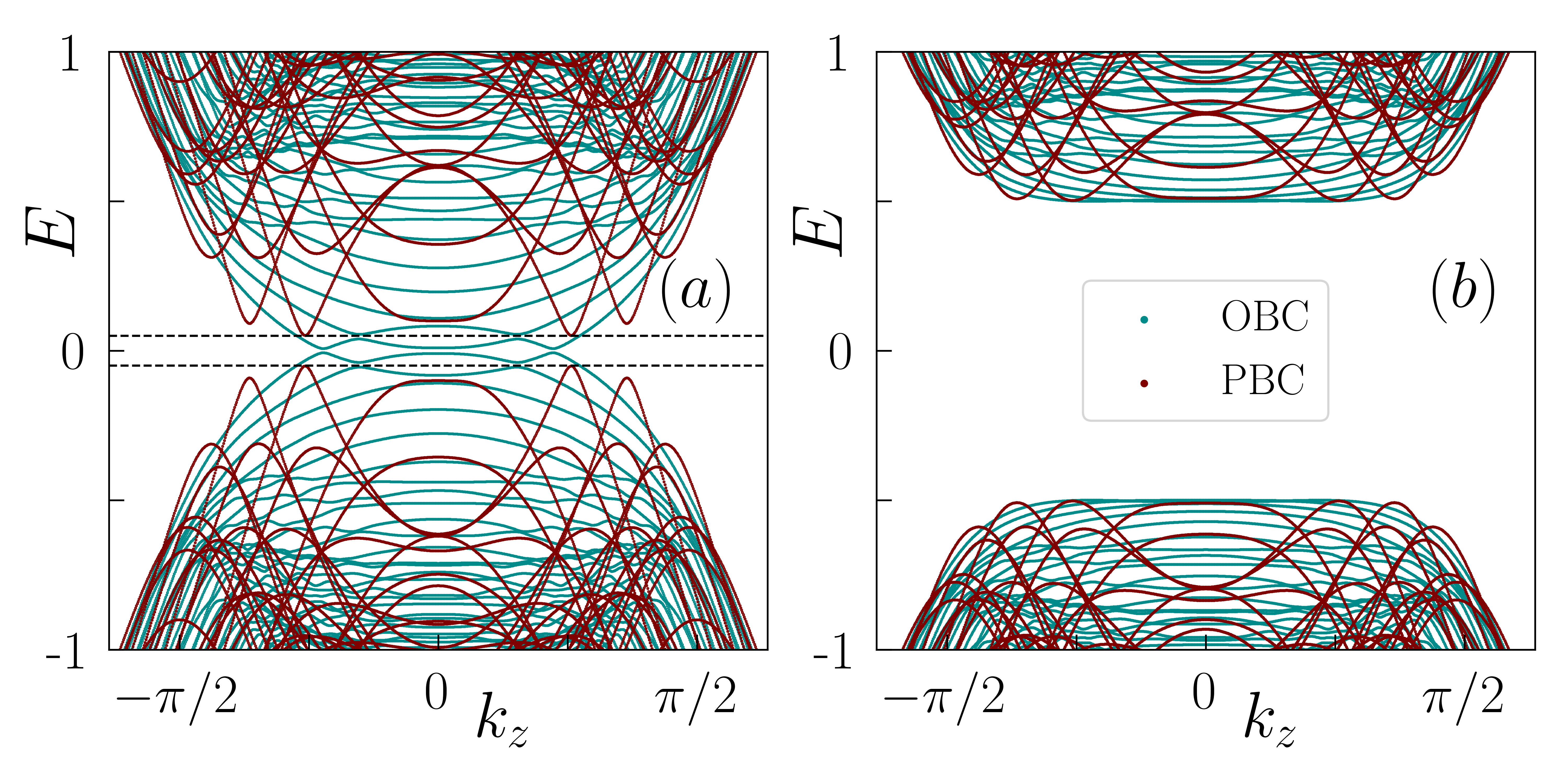
For the WSM NW, we consider and numerically diagonalize the above Hamiltonian for each value of . We present the eigen spectrum as a function of in Fig. 4(a) employing both PBC and OBC. As mentioned earlier, in OBC,‘ we obtain the information about both bulk and surface states of the system while in PBC information about only the bulk states can be achieved.
For TRS-broken WSM NW, it has already been shown in Ref. [Kaladzhyan and Bardarson, 2019] that the bulk states are gapped out due to the finite size effect, and within the bulk gap, , only surface states exist. A finite size gap, , is also developed on the surface state spectrum but the bulk confinement gap is larger than that of developed in the surface. Specifically, whereas . This feature is also observed in the present model where the bulk gap and and within the energy regime, , only surface states are present (shown in brown color in Fig. 4(a)). This behaviour is not present in the slab geometry where both the bulk and surface states are gapless, and thus distingusing the surface states from the bulk do not seem posible in the WSM slab. Therefore NW geometry is the possible platform where the surface states can be clearly distinguished from the bulk states and can possibly be probed in such a way that the contribution of the bulk states in the measurement can be excluded.
II.3.2 WSC NW
After explaining the nature of FAs in WSM NW, let us discuss the effect of superconductivity in the NW geometry. We consider an -wave spin-singlet intra-orbital pairing with amplitude in both the bulk and surface of the NW. Since the surface states contain electrons with both spin polarizations (as shown in the slab geometry calculations), -wave spin-singlet pairing between the electrons is expected to be prominent over the spin-triplet pairing. Similar to the WSM NW, we perform the inverse FT to obtain the WSC NW Hamiltonian as,
| (12) | |||||
We then numerically diagonalize the Hamilonian considering the same system size as mentioned for the WSM NW and plot the band structure as a function of in Fig. 4(b) employing both OBC and PBC. We observe that due to the superconducting correlation, both bulk and surface states acquire a gap of magnitude .
III Conductance
In this section, we present our numerical results for the conductance in WSM and WSM/WSC NW setup.
III.1 WSM NW
Let us begin by analyzing the transport signatures of FAs in an ISB WSM NW based two-terminal setup. For this purpose, we first exclude the WSC NW part in Fig. 1(b) by extending the WSM NW and attach two semi-infinite leads at and . We model both the leads using the same Hamiltonian which is used to describe the WSM NW. The chemical potential at the left (right) lead is fixed at (). Under the application of voltage bias, , we compute two-terminal charge transport employing Landauer formula Datta (1995). To obtain the current traversing through the NW, we first construct the scattering matrix, which relates the incoming propagating modes to the outgoing modes in the leads with the central WSM NW being considered as the scatterer. Incoming, outgoing states and the scattering matrix are defined as:
| (13) | |||||
| (14) |
,
where, is the incoming state from the left (right) lead in the mode. Here, is the number of occupied modes/channels in the left (right) lead for a given voltage bias . Similarly, is the outgoing state into the left (right) lead in the mode after the scattering event takes place. Here, ‘’ denotes the tranpose operation. The unitary scattering matrix of dimension reads
| (15) |
where, is a square matrix of dimension and is a matrix of dimension . Physically, represents the reflection matrix with elements being the amplitude of reflection from the mode to the -mode in the left (right) lead. Similarly, represents the transmission matrix with elements denoting the amplitude of the transmission from the mode in left (right) lead to the mode in the right (left) lead following the unitarity condition: . Within this formalism, the two-terminal conductance at zero temperature can be obtained using the Landauer formula given by Datta (1995),
| (16) |
where, is the unit of quantum conductance. The scattering amplitudes can be calculated numerically using python package KWANT Groth et al. (2014).
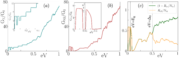
We depict the two-terminal conductance in WSM NW setup in units of quantum conductance as a function of voltage bias, , in Fig. 5(a) assuming the length along -direction is lattice sites. We observe that conductance initially increases in steps of and a plateau-like behaviour appears after that. For a more clear understanding we refer to the inset of Fig. 5(a). However, when we increase the bias voltage, the step-like behaviour is lost and a continuous enhancement in conductance is observed. Similiar behaviour of the conductance has also been observed for TRS-broken WSM NW Kaladzhyan and Bardarson (2019). Interestingly, in case of ISB WSM NW, the quantization of the conductance occurs in steps of , whereas in case of TRS-broken WSM NW, the steps appear in units of as shown in Ref. [Kaladzhyan and Bardarson, 2019]. This happens due to the presence of four FAs (two on each surface) in such system as compared to TRS-broken WSM where two FAs are present. The step-like behaviour appears due to the FA surface states within the finite size gap in the system, while the following continuous enhancement happens since the bulk states start contributing. Due to semimetallic nature of the bulk spectrum, the conductance for the higher bias voltages varies as .
In clean systems, the conductance does not depend on the length of the WSM NW along the -direction because of phase coherent transport along the NW axis considering the same Hamiltonian for the leads. Increasing the system size along the transverse directions do not affect the qualitative picture of the conductance plot, but the quantitative behaviour of the conductance changes since both and decrease. Additionally, increasing the value of and usually enhances the number of transverse modes in the lead spectrum. Hence, the occupancy of propagating modes increases within the leads for a given voltage bias, which in turn can enhance the conductance according to Eq. (16).
III.2 WSM/WSC NW
Here, we discuss another main finding of our analysis which deals with the transport signatures of the FAs in WSM/WSC NW hybrid junction. For this purpose, we consider the geometry shown in Fig. 1(b) under the application of voltage bias . We model this hybrid setup using the Hamiltonian in Eq. (12). The uniform superconducting pairing potential is chosen as,
| (17) |
The leads are also modelled by the same Hamiltonian as mentioned in Eq. (12). The left lead is chosen to be nonsuperconducting (), while the right lead possesses a superconding pairing gap as mentioned above. This hybrid setup mimics a normal-superconductor (NS) junction.
The additional mechanism that comes into play while considering charge transport in such superconducting hybrid junction, is the Andreev reflection (AR) where an incoming right moving electron from the left lead with spin combines with another electron with oppsosite spin to form a spin-singlet Cooper pair (CP) leaving behind a hole that reflects back from the interface. The CPs, formed at the interface, propagates through the WSC and give rises to supercurrent Blonder et al. (1982). In our work, the primary motivation to capture the signatures of FAs via the AR lies into these spin textures of the FAs [see Fig. 3(a)-(c)]. Note that, within a particular surface, the spin polarization of electrons along the -direction has components along both positive and negative -axis, indicating the strong possibility of AR mediated via the FAs.
To find the conductance in this hybrid junction, we employ the scattering matrix formalism which now takes more complex form compared to the bare WSM NW due to the presence of the AR process. It can now be written as
| (18) |
where, is a column matrix of dimension and it represents the incoming electron (hole) from the left (right) lead. Similarly, designates the outgoing electron (hole) in the left (right) lead. The scattering matrix can be written as
| (19) |
where, and denote the complex matrices with dimension . The matrix element represents the amplitude of reflection from the particle type- in the channel of left lead to the particle type- in the channel of left lead with . For our purpose, it is now sufficient to focus on the reflection matrices in the left lead i.e.,
| (20) |
The reason behind writing Eq. (20) is the absence of the quasiparticle states within the superconducting gap which prevents the transmission of electron like (or hole like) particles from the left normal lead to the right superconducting lead. Similarly, there are no single particle states present inside the right lead to propagate through the WSC and reach the left lead. In this circumstance, within the subgap regime, the only possible scattering processes are: reflection of electrons as an electron (normal reflection), denoted by matrix in Eq. (20), and AR. Note that, it follows the unitarity relation of as given by
| (21) |
With this understanding, we now employ the BTK formalism to obtain the conductance of this hybrid junction as Blonder et al. (1982); Dumitrescu et al. (2015); Rosdahl et al. (2018); Das Sarma et al. (2016)
| (22) |
where, and . is the number of occupied modes/channels in the left lead for a given voltage bias . Using the python package KWANT Groth et al. (2014), we obtain the reflection matrices, , and also to compute the conductance.
We depict the conductance, , as a function of voltage bias, , in Fig. 5(b). We also show and for comparison, normalized by the number of available modes in left lead (), as a function of in Fig. 5(c). For the bias voltage less than the bulk confinement gap () where only the FA surface states exist (see Fig.4(a)), we find exhibits nonzero value and becomes almost equal to (see Fig. 5(b)). This is concomitant with nonzero value of (see Fig. 5(c)) which establishes the possibility of AR mediated by FAs which is one of the main claims of the present work: capturing the signatures of FAs in this superconducting hybrid junction. In the subgapped regime (), and identically follow each other which can be explained using the unitarity relation of [see Eq. (21)] as, . For , we observe suddenly drops to zero and then gradually increases with the voltage bias as shown in Fig. 5(b). For better clarity, we also refer to the inset of Fig. 5(b). When , and decays with the increase in voltage bias. This is due to the presence of finite quasiparticle density of states for , which allows and matrices to be nonzero, and as a result, Eq. (21) does not hold.
Interestingly, in the subgapped regime, is not quantized in the regime where exhibits quantized values as shown in the inset of Fig. 5(a). This is unusual since in the absence of any interfacial insulating barrier (transparnent limit), the subgap condutance is expected to be twice of the conductance in the absence of the superconductors i.e., (see Ref. [Blonder et al., 1982] for details). This pecularity can originate from two correlated reasons as follows. First: even though FAs host both up and down spin textures, the expectation value of spin polarization, , for all states on the FAs. This makes the AR deviated from the unit probability within the subgap regime even in the transparent limit which indicates that all the electrons may not reflect as holes from the interface. Thus, perfect AR does not take place restricting the quantization of . Second: In Fig. 5(c), we note that a finite value of (since is quantized in the region of concern) even in the absence of any insulating barrier at the interface. Such normal reflection probability can originate from the inter-channel scatterings in the WSM NW which can also prohibit the perfect quantization.
IV Stability against disorder
So far, all the results are presented for clean systems. We now extend our analysis to include the effect of disorder and investigate the robustness of our results in both WSM NW and WSM/WSC NW junction. Usually, the bulk properties of WSM are robust against disorder unless the disorder strength is strong enough to allow inter-node scatterings and create a gap to destroy the topological phase Shapourian and Hughes (2016); Klier et al. (2019); Chen et al. (2015); Altland and Bagrets (2016). Specifically, to check the stability of FAs against the disorder that breaks translational symmetry of the system, we consider random quenched disorder which are delta-correlated, in terms of a onsite energy potentials in the Hamiltonian as,
| (23) |
where, is random number uniformly distributed in the range and is referred as the disorder strength. We choose for WSM NW and for WSM/WSC NW junction. For the hybrid junction, the disorder is considered only in region Beenakker (1992); Takagaki and Takayanagi (1996); Pientka et al. (2012).
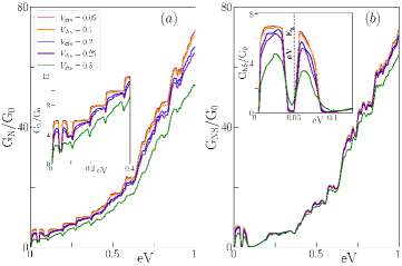
To compute the conductance, and (Eq. (16) and Eq. (22)), in the presence of disorder, we again employ scattering matrix formalism and extract the reflection () and transmission () matrices using KWANT Groth et al. (2014). We show the disorder averaged conductance, and , as a function of voltage bias for various disorder strengths in Fig. 6() and () respectively. The results are obtained after averaging over 30 disorder configurations.
The average energy level spacing of the FAs in the WSM NW geometry is estimated approximately as where the average level broadening induced by disorder is, Kaladzhyan and Bardarson (2019). From here, we can estimate the critical disorder strength above which quantized conductance plateau does not survive as, . From Fig. 6(a) and Fig. 6(b), we can verify that quantized conductance plateau, arising due to the FA surface states, survive upto the disorder strength, , (see the inset of Fig. 6(a) for better clarity) above which the conductance quantization is diminished. Similarly, in the case of the WSM/WSC NW junction, we observe our results to sustain upto sufficiently large disorder strength. Note that, unlike the clean system, where the conductance is independent of NW length, in the presence of disorder, conductance depends on the NW length since phase coherency is lost. In particular, keeping the disorder strength moderate, the conductance decreases as the NW length is increased.
V Summary and Conclusions
To summarize, in this article, we have explored an ISB WSM with four bulk Weyl nodes in plane. We have analyzed the properties of FAs in a slab geometry considering -direction to be finite and found both up and down spin-polarized FA states at both and surfaces. We have then investigated the FAs with further confinement in another direction which leads to a NW geometry. In WSM NW setup, due to the finite size effects, both the bulk and surface states are gapped out. Interestingly, the surface state gap is still smaller than the bulk confinement gap, thus allowing one to probe only surface states and explore various transport signatures due to FAs only. We have extracted the matrix elements within the scattering matrix formalism using the python package KWANT Groth et al. (2014). Specifically, we have computed the two-terminal conductance of the WSM NW using the Landauer formula and observed the conductance quantization in units of . To capture the signatures of FAs in AR, we have constructed a WSM/WSC NW hybrid junction and found the conductance using the BTK formula Blonder et al. (1982); Das Sarma et al. (2016); Dumitrescu et al. (2015); Rosdahl et al. (2018). We show that the signatures of the FAs can be separated out via the AR process too. Note that, the conductance in this hybrid setup is not quantized. Finally, we have investigated the stability of the conductance against random onsite disorder potential in both WSM NW and WSM/WSC NW hybrid junction and find our results to be robust against disorder strength upto a critical value .
Here we convey few comments as far as the experimental feasibility of our transport setups are concerned. Earlier theoretical works to capture the signature of FAs are mainly based on TRS-broken WSM Baum et al. (2015); Kaladzhyan and Bardarson (2019); Mukherjee et al. (2018). In reality, TRS-broken WSM needs application of large magnetic field Xiong et al. (2015), whereas experimentally observed WSM phases are mostly ISB e.g. TaAs, TaP, NbAs, NbP etc. Lv et al. (2015a, b, c); Lu et al. (2015); Xu et al. (2015a, b, c); Soluyanov et al. (2015); Moll et al. (2016); Wang et al. (2016a); Xu et al. (2015d); Ojanen (2013); Sun et al. (2015a); Feng et al. (2016); Xu et al. (2016); Potter et al. (2014). Specifically, there exists several works on Dirac semimetal, , NW where WSM phase can be achieved by applying a strong external magnetic field ( Tesla) with diameter of the NW nm Wang et al. (2018); Lin et al. (2017); Li et al. (2015); Wang et al. (2016b). Application of large external magnetic field can generate Landau levels and the phenomenon of chiral anomaly may affect the results. Hence, our work based on ISB WSM NW is out of such scope and carries potential from the practical point of view. Note that, the bulk gap in NW due to quantum confinement is observed to be meV with gap size being ( being the Fermi velocity and cross section of the NW respectively). For a typical value of in NW and (for lattice constant ), gap size comes out to be which closely resembles the bulk confinement gap, (assuming eV), obtained in our numerical calculation of band structure. Therefore, the realization of our theoretical results regarding FA mediated transport is subjected to the chemical potential lying within the bulk confinement gap, i.e. . Finally, the realization of a WSC can be achieved by introducing a common -wave superconductor like Al or Nb in close proximity to the WSM NW Bachmann et al. (2017). Thus, our proposal serves as a possible potential experimental testbed, offering experimentalists the opportunity and challenge to validate our findings.
Acknowledgements
A. P. acknowledges Arijit Kundu, Sourin Das, Arnob Kumar Ghosh, and Pritam Chatterjee for stimulating discussions. A. P. and A. S. acknowledge SAMKHYA: High-Performance Computing facility provided by Institute of Physics, Bhubaneswar, for numerical computations. P. D. acknowledges Department of Space, Government of India for all supports at Physical Research Laboratory (PRL) and Department of Science and Technology (DST), India (through SERB Start-up Research Grant (File no. SRG/2022/001121)) for the financial support.
References
- Armitage et al. (2018) N. P. Armitage, E. J. Mele, and A. Vishwanath, “Weyl and dirac semimetals in three-dimensional solids,” Rev. Mod. Phys. 90, 015001 (2018).
- Rao (2016) S. Rao, “Weyl semi-metals: A short review,” Journal of the Indian Institute of Science 96, 145–156 (2016).
- McCormick et al. (2017) T. M. McCormick, I. Kimchi, and N. Trivedi, “Minimal models for topological weyl semimetals,” Phys. Rev. B 95, 075133 (2017).
- Yan and Felser (2017) B. Yan and C. Felser, “Topological materials: Weyl semimetals,” Annual Review of Condensed Matter Physics 8, 337–354 (2017).
- Burkov (2018) A. Burkov, “Weyl metals,” Annual Review of Condensed Matter Physics 9, 359–378 (2018).
- Dirac and Fowler (1928) P. A. M. Dirac and R. H. Fowler, “The quantum theory of the electron,” Proceedings of the Royal Society of London. Series A, Containing Papers of a Mathematical and Physical Character 117, 610–624 (1928).
- Weyl (1929) H. Weyl, “Elektron und gravitation. i,” Zeitschrift für Physik 56, 330–352 (1929).
- Murakami (2007) S. Murakami, “Phase transition between the quantum spin hall and insulator phases in 3d: emergence of a topological gapless phase,” New Journal of Physics 9, 356 (2007).
- Vazifeh and Franz (2013) M. M. Vazifeh and M. Franz, “Electromagnetic response of weyl semimetals,” Phys. Rev. Lett. 111, 027201 (2013).
- Burkov and Balents (2011) A. A. Burkov and L. Balents, “Weyl semimetal in a topological insulator multilayer,” Phys. Rev. Lett. 107, 127205 (2011).
- Burkov et al. (2011) A. A. Burkov, M. D. Hook, and L. Balents, “Topological nodal semimetals,” Phys. Rev. B 84, 235126 (2011).
- Zyuzin et al. (2012) A. A. Zyuzin, S. Wu, and A. A. Burkov, “Weyl semimetal with broken time reversal and inversion symmetries,” Phys. Rev. B 85, 165110 (2012).
- Zyuzin and Burkov (2012) A. A. Zyuzin and A. A. Burkov, “Topological response in weyl semimetals and the chiral anomaly,” Phys. Rev. B 86, 115133 (2012).
- Halász and Balents (2012) G. B. Halász and L. Balents, “Time-reversal invariant realization of the weyl semimetal phase,” Phys. Rev. B 85, 035103 (2012).
- Liu et al. (2013) C.-X. Liu, P. Ye, and X.-L. Qi, “Chiral gauge field and axial anomaly in a weyl semimetal,” Phys. Rev. B 87, 235306 (2013).
- Wan et al. (2011) X. Wan, A. M. Turner, A. Vishwanath, and S. Y. Savrasov, “Topological semimetal and fermi-arc surface states in the electronic structure of pyrochlore iridates,” Phys. Rev. B 83, 205101 (2011).
- Bzdušek et al. (2015) T. c. v. Bzdušek, A. Rüegg, and M. Sigrist, “Weyl semimetal from spontaneous inversion symmetry breaking in pyrochlore oxides,” Phys. Rev. B 91, 165105 (2015).
- Witczak-Krempa and Kim (2012) W. Witczak-Krempa and Y. B. Kim, “Topological and magnetic phases of interacting electrons in the pyrochlore iridates,” Phys. Rev. B 85, 045124 (2012).
- Lv et al. (2015a) B. Q. Lv, N. Xu, H. M. Weng, J. Z. Ma, P. Richard, X. C. Huang, L. X. Zhao, G. F. Chen, C. E. Matt, F. Bisti, V. N. Strocov, J. Mesot, Z. Fang, X. Dai, T. Qian, M. Shi, and H. Ding, “Observation of weyl nodes in taas,” Nature Physics 11, 724–727 (2015a).
- Lv et al. (2015b) B. Q. Lv, H. M. Weng, B. B. Fu, X. P. Wang, H. Miao, J. Ma, P. Richard, X. C. Huang, L. X. Zhao, G. F. Chen, Z. Fang, X. Dai, T. Qian, and H. Ding, “Experimental discovery of weyl semimetal taas,” Phys. Rev. X 5, 031013 (2015b).
- Lv et al. (2015c) B. Q. Lv, S. Muff, T. Qian, Z. D. Song, S. M. Nie, N. Xu, P. Richard, C. E. Matt, N. C. Plumb, L. X. Zhao, G. F. Chen, Z. Fang, X. Dai, J. H. Dil, J. Mesot, M. Shi, H. M. Weng, and H. Ding, “Observation of fermi-arc spin texture in taas,” Phys. Rev. Lett. 115, 217601 (2015c).
- Lu et al. (2015) L. Lu, Z. Wang, D. Ye, L. Ran, L. Fu, J. D. Joannopoulos, and M. Soljačić, “Experimental observation of weyl points,” Science 349, 622–624 (2015).
- Xu et al. (2015a) S.-Y. Xu, I. Belopolski, D. S. Sanchez, C. Zhang, G. Chang, C. Guo, G. Bian, Z. Yuan, H. Lu, T.-R. Chang, P. P. Shibayev, M. L. Prokopovych, N. Alidoust, H. Zheng, C.-C. Lee, S.-M. Huang, R. Sankar, F. Chou, C.-H. Hsu, H.-T. Jeng, A. Bansil, T. Neupert, V. N. Strocov, H. Lin, S. Jia, and M. Z. Hasan, “Experimental discovery of a topological weyl semimetal state in tap,” Science Advances 1, e1501092 (2015a).
- Xu et al. (2015b) S.-Y. Xu, N. Alidoust, I. Belopolski, Z. Yuan, G. Bian, T.-R. Chang, H. Zheng, V. N. Strocov, D. S. Sanchez, G. Chang, C. Zhang, D. Mou, Y. Wu, L. Huang, C.-C. Lee, S.-M. Huang, B. Wang, A. Bansil, H.-T. Jeng, T. Neupert, A. Kaminski, H. Lin, S. Jia, and M. Zahid Hasan, “Discovery of a weyl fermion state with fermi arcs in niobium arsenide,” Nature Physics 11, 748–754 (2015b).
- Xu et al. (2015c) S.-Y. Xu, I. Belopolski, N. Alidoust, M. Neupane, G. Bian, C. Zhang, R. Sankar, G. Chang, Z. Yuan, C.-C. Lee, S.-M. Huang, H. Zheng, J. Ma, D. S. Sanchez, B. Wang, A. Bansil, F. Chou, P. P. Shibayev, H. Lin, S. Jia, and M. Z. Hasan, “Discovery of a weyl fermion semimetal and topological fermi arcs,” Science 349, 613–617 (2015c).
- Soluyanov et al. (2015) A. A. Soluyanov, D. Gresch, Z. Wang, Q. Wu, M. Troyer, X. Dai, and B. A. Bernevig, “Type-ii weyl semimetals,” Nature 527, 495–498 (2015).
- Moll et al. (2016) P. J. W. Moll, N. L. Nair, T. Helm, A. C. Potter, I. Kimchi, A. Vishwanath, and J. G. Analytis, “Transport evidence for fermi-arc-mediated chirality transfer in the dirac semimetal cd3as2,” Nature 535, 266–270 (2016).
- Wang et al. (2016a) Z. Wang, M. G. Vergniory, S. Kushwaha, M. Hirschberger, E. V. Chulkov, A. Ernst, N. P. Ong, R. J. Cava, and B. A. Bernevig, “Time-reversal-breaking weyl fermions in magnetic heusler alloys,” Phys. Rev. Lett. 117, 236401 (2016a).
- Xu et al. (2015d) D.-F. Xu, Y.-P. Du, Z. Wang, Y.-P. Li, X.-H. Niu, Q. Yao, D. Pavel, Z.-A. Xu, X.-G. Wan, and D.-L. Feng, “Observation of fermi arcs in non-centrosymmetric weyl semi-metal candidate nbp*,” Chinese Physics Letters 32, 107101 (2015d).
- Ojanen (2013) T. Ojanen, “Helical fermi arcs and surface states in time-reversal invariant weyl semimetals,” Phys. Rev. B 87, 245112 (2013).
- Sun et al. (2015a) Y. Sun, S.-C. Wu, and B. Yan, “Topological surface states and fermi arcs of the noncentrosymmetric weyl semimetals taas, tap, nbas, and nbp,” Phys. Rev. B 92, 115428 (2015a).
- Feng et al. (2016) B. Feng, Y.-H. Chan, Y. Feng, R.-Y. Liu, M.-Y. Chou, K. Kuroda, K. Yaji, A. Harasawa, P. Moras, A. Barinov, W. Malaeb, C. Bareille, T. Kondo, S. Shin, F. Komori, T.-C. Chiang, Y. Shi, and I. Matsuda, “Spin texture in type-ii weyl semimetal ,” Phys. Rev. B 94, 195134 (2016).
- Xu et al. (2016) S.-Y. Xu, I. Belopolski, D. S. Sanchez, M. Neupane, G. Chang, K. Yaji, Z. Yuan, C. Zhang, K. Kuroda, G. Bian, C. Guo, H. Lu, T.-R. Chang, N. Alidoust, H. Zheng, C.-C. Lee, S.-M. Huang, C.-H. Hsu, H.-T. Jeng, A. Bansil, T. Neupert, F. Komori, T. Kondo, S. Shin, H. Lin, S. Jia, and M. Z. Hasan, “Spin polarization and texture of the fermi arcs in the weyl fermion semimetal taas,” Phys. Rev. Lett. 116, 096801 (2016).
- Potter et al. (2014) A. C. Potter, I. Kimchi, and A. Vishwanath, “Quantum oscillations from surface fermi arcs in weyl and dirac semimetals,” Nature Communications 5, 5161 (2014).
- Altland and Bagrets (2016) A. Altland and D. Bagrets, “Theory of the strongly disordered weyl semimetal,” Phys. Rev. B 93, 075113 (2016).
- Shapourian and Hughes (2016) H. Shapourian and T. L. Hughes, “Phase diagrams of disordered weyl semimetals,” Phys. Rev. B 93, 075108 (2016).
- Klier et al. (2019) J. Klier, I. V. Gornyi, and A. D. Mirlin, “From weak to strong disorder in weyl semimetals: Self-consistent born approximation,” Phys. Rev. B 100, 125160 (2019).
- Sbierski et al. (2014) B. Sbierski, G. Pohl, E. J. Bergholtz, and P. W. Brouwer, “Quantum transport of disordered weyl semimetals at the nodal point,” Phys. Rev. Lett. 113, 026602 (2014).
- Chen et al. (2015) C.-Z. Chen, J. Song, H. Jiang, Q.-f. Sun, Z. Wang, and X. C. Xie, “Disorder and metal-insulator transitions in weyl semimetals,” Phys. Rev. Lett. 115, 246603 (2015).
- Maciejko and Nandkishore (2014) J. Maciejko and R. Nandkishore, “Weyl semimetals with short-range interactions,” Phys. Rev. B 90, 035126 (2014).
- Witczak-Krempa et al. (2014) W. Witczak-Krempa, M. Knap, and D. Abanin, “Interacting weyl semimetals: Characterization via the topological hamiltonian and its breakdown,” Phys. Rev. Lett. 113, 136402 (2014).
- Hosseini and Askari (2015) M. V. Hosseini and M. Askari, “Ruderman-kittel-kasuya-yosida interaction in weyl semimetals,” Phys. Rev. B 92, 224435 (2015).
- Jacobs et al. (2016) V. P. J. Jacobs, P. Betzios, U. Gürsoy, and H. T. C. Stoof, “Electromagnetic response of interacting weyl semimetals,” Phys. Rev. B 93, 195104 (2016).
- Laubach et al. (2016) M. Laubach, C. Platt, R. Thomale, T. Neupert, and S. Rachel, “Density wave instabilities and surface state evolution in interacting weyl semimetals,” Phys. Rev. B 94, 241102 (2016).
- Roy et al. (2017) B. Roy, P. Goswami, and V. Juričić, “Interacting weyl fermions: Phases, phase transitions, and global phase diagram,” Phys. Rev. B 95, 201102 (2017).
- Boettcher (2020) I. Boettcher, “Interplay of topology and electron-electron interactions in rarita-schwinger-weyl semimetals,” Phys. Rev. Lett. 124, 127602 (2020).
- Xu et al. (2011) G. Xu, H. Weng, Z. Wang, X. Dai, and Z. Fang, “Chern semimetal and the quantized anomalous hall effect in ,” Phys. Rev. Lett. 107, 186806 (2011).
- Sun et al. (2015b) Y. Sun, S.-C. Wu, and B. Yan, “Topological surface states and fermi arcs of the noncentrosymmetric weyl semimetals taas, tap, nbas, and nbp,” Phys. Rev. B 92, 115428 (2015b).
- Sun et al. (2015c) Y. Sun, S.-C. Wu, M. N. Ali, C. Felser, and B. Yan, “Prediction of weyl semimetal in orthorhombic ,” Phys. Rev. B 92, 161107 (2015c).
- Wang et al. (2018) S. Wang, B.-C. Lin, W.-Z. Zheng, D. Yu, and Z.-M. Liao, “Fano interference between bulk and surface states of a dirac semimetal nanowire,” Phys. Rev. Lett. 120, 257701 (2018).
- Chen et al. (2020) G. Chen, W. Chen, and O. Zilberberg, “Field-effect transistor based on surface negative refraction in Weyl nanowire,” APL Materials 8, 011102 (2020).
- Li et al. (2015) C.-Z. Li, L.-X. Wang, H. Liu, J. Wang, Z.-M. Liao, and D.-P. Yu, “Giant negative magnetoresistance induced by the chiral anomaly in individual cd3as2 nanowires,” Nature Communications 6, 10137 (2015).
- Baireuther et al. (2016) P. Baireuther, J. A. Hutasoit, J. Tworzydło, and C. W. J. Beenakker, “Scattering theory of the chiral magnetic effect in a weyl semimetal: interplay of bulk weyl cones and surface fermi arcs,” New Journal of Physics 18, 045009 (2016).
- Gorbar et al. (2016) E. V. Gorbar, V. A. Miransky, I. A. Shovkovy, and P. O. Sukhachov, “Origin of dissipative fermi arc transport in weyl semimetals,” Phys. Rev. B 93, 235127 (2016).
- Igarashi and Koshino (2017) A. Igarashi and M. Koshino, “Magnetotransport in weyl semimetal nanowires,” Phys. Rev. B 95, 195306 (2017).
- Breitkreiz and Brouwer (2019) M. Breitkreiz and P. W. Brouwer, “Large contribution of fermi arcs to the conductivity of topological metals,” Phys. Rev. Lett. 123, 066804 (2019).
- Mukherjee et al. (2018) D. K. Mukherjee, S. Rao, and S. Das, “Fabry perot interferometry in weyl semi-metals,” Journal of Physics: Condensed Matter 31, 045302 (2018).
- Kaladzhyan and Bardarson (2019) V. Kaladzhyan and J. H. Bardarson, “Quantized fermi arc mediated transport in weyl semimetal nanowires,” Phys. Rev. B 100, 085424 (2019).
- Meng and Balents (2012) T. Meng and L. Balents, “Weyl superconductors,” Phys. Rev. B 86, 054504 (2012).
- Cho et al. (2012) G. Y. Cho, J. H. Bardarson, Y.-M. Lu, and J. E. Moore, “Superconductivity of doped weyl semimetals: Finite-momentum pairing and electronic analog of the 3he- phase,” Phys. Rev. B 86, 214514 (2012).
- Uchida et al. (2014) S. Uchida, T. Habe, and Y. Asano, “Andreev reflection in weyl semimetals,” Journal of the Physical Society of Japan 83, 064711 (2014).
- Khanna et al. (2016) U. Khanna, D. K. Mukherjee, A. Kundu, and S. Rao, “Chiral nodes and oscillations in the josephson current in weyl semimetals,” Phys. Rev. B 93, 121409 (2016).
- Mukherjee et al. (2017) D. K. Mukherjee, S. Rao, and A. Kundu, “Transport through andreev bound states in a weyl semimetal quantum dot,” Phys. Rev. B 96, 161408 (2017).
- Zhang et al. (2018a) S.-B. Zhang, J. Erdmenger, and B. Trauzettel, “Chirality josephson current due to a novel quantum anomaly in inversion-asymmetric weyl semimetals,” Phys. Rev. Lett. 121, 226604 (2018a).
- Zhang et al. (2018b) S.-B. Zhang, F. Dolcini, D. Breunig, and B. Trauzettel, “Appearance of the universal value of the zerobias conductance in a weyl semimetalsuperconductor junction,” Phys. Rev. B 97, 041116 (2018b).
- Saxena et al. (2023) R. Saxena, N. Basak, P. Chatterjee, S. Rao, and A. Saha, “Thermoelectric properties of inversion symmetry broken weyl semimetal–weyl superconductor hybrid junctions,” Phys. Rev. B 107, 195426 (2023).
- Dutta et al. (2020) P. Dutta, F. Parhizgar, and A. M. Black-Schaffer, “Finite bulk josephson currents and chirality blockade removal from interorbital pairing in magnetic weyl semimetals,” Phys. Rev. B 101, 064514 (2020).
- (68) P. Chatterjee and P. Dutta, “Quasiparticles-mediated thermal diode effect in weyl josephson junctions,” arXiv:2312.05008 [cond-mat.supr-con] .
- Khanna et al. (2014) U. Khanna, A. Kundu, S. Pradhan, and S. Rao, “Proximity-induced superconductivity in weyl semimetals,” Phys. Rev. B 90, 195430 (2014).
- Bednik et al. (2015) G. Bednik, A. A. Zyuzin, and A. A. Burkov, “Superconductivity in weyl metals,” Phys. Rev. B 92, 035153 (2015).
- Chen and Franz (2016) A. Chen and M. Franz, “Superconducting proximity effect and majorana flat bands at the surface of a weyl semimetal,” Phys. Rev. B 93, 201105 (2016).
- Baireuther et al. (2017) P. Baireuther, J. Tworzydlo, M. Breitkreiz, I. Adagideli, and C. W. J. Beenakker, “Weylmajorana solenoid,” New Journal of Physics 19, 025006 (2017).
- Dutta and Black-Schaffer (2019) P. Dutta and A. M. Black-Schaffer, “Signature of odd-frequency equal-spin triplet pairing in the josephson current on the surface of weyl nodal loop semimetals,” Phys. Rev. B 100, 104511 (2019).
- Faraei and Jafari (2019) Z. Faraei and S. A. Jafari, “Induced superconductivity in fermi arcs,” Phys. Rev. B 100, 035447 (2019).
- Zheng et al. (2021) Y. Zheng, W. Chen, and D. Y. Xing, “Andreev reflection in fermi-arc surface states of weyl semimetals,” Phys. Rev. B 104, 075420 (2021).
- Baum et al. (2015) Y. Baum, E. Berg, S. A. Parameswaran, and A. Stern, “Current at a distance and resonant transparency in weyl semimetals,” Phys. Rev. X 5, 041046 (2015).
- (77) K. Pareek and A. Kundu, “Quantum transport simulation of non-local response in weyl semimetals,” arXiv:1812.05504 [cond-mat.mes-hall] .
- (78) R. Kumari, D. K. Mukherjee, and A. Kundu, “Fermi-arcs mediated transport in surface josephson junctions of weyl semimetal,” arXiv:2401.14956 [cond-mat.mes-hall] .
- Kuibarov et al. (2024) A. Kuibarov, O. Suvorov, R. Vocaturo, A. Fedorov, R. Lou, L. Merkwitz, V. Voroshnin, J. I. Facio, K. Koepernik, A. Yaresko, G. Shipunov, S. Aswartham, J. v. d. Brink, B. Büchner, and S. Borisenko, “Evidence of superconducting fermi arcs,” Nature 626, 294–299 (2024).
- Sekine and Nomura (2013) A. Sekine and K. Nomura, “Electron correlation induced spontaneous symmetry breaking and weyl semimetal phase in a strongly spin–orbit coupled system,” Journal of the Physical Society of Japan 82, 033702 (2013).
- Qin et al. (2019) W. Qin, L. Li, and Z. Zhang, “Chiral topological superconductivity arising from the interplay of geometric phase and electron correlation,” Nature Physics 15, 796–802 (2019).
- Kourtis et al. (2016) S. Kourtis, J. Li, Z. Wang, A. Yazdani, and B. A. Bernevig, “Universal signatures of fermi arcs in quasiparticle interference on the surface of weyl semimetals,” Phys. Rev. B 93, 041109 (2016).
- Datta (1995) S. Datta, Electronic Transport in Mesoscopic Systems, Cambridge Studies in Semiconductor Physics and Microelectronic Engineering (Cambridge University Press, 1995).
- Groth et al. (2014) C. W. Groth, M. Wimmer, A. R. Akhmerov, and X. Waintal, “Kwant: a software package for quantum transport,” New Journal of Physics 16, 063065 (2014).
- Blonder et al. (1982) G. E. Blonder, M. Tinkham, and T. M. Klapwijk, “Transition from metallic to tunneling regimes in superconducting microconstrictions: Excess current, charge imbalance, and supercurrent conversion,” Phys. Rev. B 25, 4515–4532 (1982).
- Dumitrescu et al. (2015) E. Dumitrescu, B. Roberts, S. Tewari, J. D. Sau, and S. Das Sarma, “Majorana fermions in chiral topological ferromagnetic nanowires,” Phys. Rev. B 91, 094505 (2015).
- Rosdahl et al. (2018) T. O. Rosdahl, A. Vuik, M. Kjaergaard, and A. R. Akhmerov, “Andreev rectifier: A nonlocal conductance signature of topological phase transitions,” Phys. Rev. B 97, 045421 (2018).
- Das Sarma et al. (2016) S. Das Sarma, A. Nag, and J. D. Sau, “How to infer non-abelian statistics and topological visibility from tunneling conductance properties of realistic majorana nanowires,” Phys. Rev. B 94, 035143 (2016).
- Beenakker (1992) C. W. J. Beenakker, “Quantum transport in semiconductor-superconductor microjunctions,” Phys. Rev. B 46, 12841–12844 (1992).
- Takagaki and Takayanagi (1996) Y. Takagaki and H. Takayanagi, “Quantized conductance in semiconductor-superconductor-junction quantum point contacts,” Phys. Rev. B 53, 14530–14533 (1996).
- Pientka et al. (2012) F. Pientka, G. Kells, A. Romito, P. W. Brouwer, and F. von Oppen, “Enhanced zero-bias majorana peak in the differential tunneling conductance of disordered multisubband quantum-wire/superconductor junctions,” Phys. Rev. Lett. 109, 227006 (2012).
- Xiong et al. (2015) J. Xiong, S. K. Kushwaha, T. Liang, J. W. Krizan, M. Hirschberger, W. Wang, R. J. Cava, and N. P. Ong, “Evidence for the chiral anomaly in the dirac semimetal na¡sub¿3¡/sub¿bi,” Science 350, 413–416 (2015).
- Lin et al. (2017) B.-C. Lin, S. Wang, L.-X. Wang, C.-Z. Li, J.-G. Li, D. Yu, and Z.-M. Liao, “Gate-tuned aharonov-bohm interference of surface states in a quasiballistic dirac semimetal nanowire,” Phys. Rev. B 95, 235436 (2017).
- Wang et al. (2016b) L.-X. Wang, C.-Z. Li, D.-P. Yu, and Z.-M. Liao, “Aharonov–bohm oscillations in dirac semimetal cd3as2 nanowires,” Nature Communications 7, 10769 (2016b).
- Bachmann et al. (2017) M. D. Bachmann, N. Nair, F. Flicker, R. Ilan, T. Meng, N. J. Ghimire, E. D. Bauer, F. Ronning, J. G. Analytis, and P. J. W. Moll, “Inducing superconductivity in weyl semimetal microstructures by selective ion sputtering,” Science Advances 3, e1602983 (2017).