Temperature dependence of the Raman spectrum of orthorhombic Bi2Se3
Abstract
Bismuth selenide, a benchmark topological insulator, grows in a trigonal structure at ambient conditions and exhibits a number of enticing properties related to the formation of Dirac surface states. Besides this polytype, a metastable orthorhombic modification with Pnma space group has been produced by electrodeposition and high-pressure high-temperature synthesis displaying upon Sb doping significant thermoelectric properties in the midtemperature range. However, very little experimental information is available on the fundamental properties of this polytype, such as, e.g., the electronic band gap and the lattice dynamics.
We report here the temperature dependence of the Raman spectra of orthorhombic Bi2Se3 between 10 K and 300 K, which displays an anharmonic behavior of the optical phonons that can be modelled with a two-phonon decay channel. In order to analyze the data we performed ab initio calculations of the electronic bandstructure, the phonon frequencies at the center of the Brillouin zone, and the phonon dispersion relations along the main symmetry directions, examining the effect of spin-orbit coupling in both phonon and electronic energies. Lastly, we report here cathodoluminescence experiments at 83 K that set a lower limit to the electronic bandgap at 0.835 eV, pointing to an indirect nature, in agreement with our calculations. These results shed light to essential properties of orthorhombic Bi2Se3 for further understanding of the potential of this semiconductor for thermoelectrics and new applications.
I Introduction
The quest for advanced materials with tailored applications has been paved with the discovery of fascinating properties, sometimes unexpectedly. One of the benchmark examples of this combination of new physics and enticing applications is the case of bismuth selenide, Bi2Se3, a three-dimensional topological insulator, i.e., a material characterized by an insulating bulk and conducting surface states. With a single Dirac cone on the Fermi surface [1], Bi2Se3 exhibits spin-momentum locking of massless helical Dirac fermions [2], due to strong spin-orbit coupling (SOC), coexisting with a two-dimensional electron gas [3], and Landau quantization of the surface states [4]. Stable in trigonal structure, Bi2Se3 has been suggested to exhibit superconducting behavior, demonstrated with Cu doping [5]. In nanoribbons it presents pronounced Aharonov-Bohm oscillations in magnetoresistance [6] that point to potential applications in future spintronic devices at room temperature. More recently, charge-current-induced of spin polarization has been detected electrically in Bi2Se3 films [7] due to locking of spin-momentum using a ferromagnetic metal tunnel barrier surface contact to measure voltage. This opens a pathway to control spin state population for potential applications in quantum computing. Moreover, Bi2Se3 films have been shown to generate a spin-transfer torque on adjacent ferromagnetic thin films [8], implying that topological insulators could facilitate efficient electrical manipulation of magnetic materials at room temperature, for example in logic and memory applications. Coupling Bi2Se3 with a ferromagnetic insulator in a bilayer system, such as EuS, has also been shown to demonstrate topologically enhanced ferromagnetism persisting up to room temperature, due to proximity coupling [9], highlighting further the potential for these applications. High-performance large-area electronics is another arena where Bi2Se3 has been proposed for applications, together with other 2D materials such as WSe2, NbSe2, In2Se3, Sb2Te3, and black phosphorus [10].
Despite this broad range of applications, thermoelectric properties are much less appealing in Bi2Se3 than in its heavier analogue, Bi2Te3. With similar trigonal structure, Bi2Te3 is known to display superior thermoelectric properties at room temperature due to the presence of six valleys for the highest valence band in the electronic bandstructure, versus only one available in Bi2Se3 [11]. This, combined with challenges to achieve p-type doped Bi2Se3, due to natural Se vacancy dominant defect chemistry, make potential thermoelectric applications only of interest at low temperatures [12] or in Bi2TexSe1-x alloys [13].
There is, however, another polytype of Bi2Se3 with orthorhombic phase, labeled hereafter as o-Bi2Se3, metastable at ambient conditions, that seems to qualify better than its trigonal counterpart for thermoelectric effects [14]. This polytype has displayed recent applications in a simultaneous heat flux and temperature acquisition dual-mode sensor [15]. The Bi2Se3 trigonal-to-orthorhombic phase transition has been shown applications in metal-dielectric-metal metamaterials with tunable negative refractive index in the near-infrared spectral region [16]. Furthermore, o-Bi2Se3 has been proposed as a promising candidate for new photovoltaic interfaces due to an excellent band energy alignment with usual photovoltaic substrates, such as TiO2 [17].
With Pnma space group, o-Bi2Se3, naturally present as a mineral named Guanajuatite [18], displays quasi one-dimensional atomic ribbons [19] and can be produced as well by quenching it from high-pressure and high-temperature growth conditions [20, 21] and by electrodeposition of thin films using electrochemical atomic layer epitaxy [22].
Despite the technological interest, o-Bi2Se3 has received much less attention from the experimental viewpoint compared to its trigonal counterpart, and many fundamental properties such as the electronic bandgap, its direct or indirect nature, and the lattice dynamics properties, such as the phonon dispersion relations, Raman spectra, and their dependence with pressure and temperature, are yet to be fully ascertain.
We report here an investigation of the temperature dependence of the Raman spectrum of o-Bi2Se3 combined with first-principles electronic and lattice dynamics calculations. The role of the anharmonicity, predicted to be larger in Pnma than in trigonal Bi2Se3 is also discussed, as well as the strength of the electron-phonon coupling, as indicated by the zero-temperature renormalization of the Raman modes. Moreover, we report here cathodoluminescence data at 83 K that enable us to provide a lower estimate of the experimental electronic bandgap, of 0.835 eV, in excellent agreement with the electronic bandstructure calculations.
These results pave the way to further experimental work towards elucidating the role of the lattice potential anharmonicity in the thermal transport, electronic, and optical properties of o-Bi2Se3.
The rest of the article is organized the following way: Section II describes the sample preparation, the experimental methods of both Raman and cathodoluminescence (CL) measurements, and the details on the ab initio calculations employed for the analysis. Section III contributes the observations made in light of the different experiments and calculations, and provides the background for the analysis of the anharmonicity of the Raman modes. This analysis is reported in Sec. IV, which is followed by some conclusions in Sec. V and the references.
II Methods
II.1 Sample preparation
The commercially available high purity (99.999%, Aldrich) Bi2Se3 powder was used for high-pressure-high-temperature synthesis of o-Bi2Se3 phase in a toroid type apparatus at P=4 GPa, T=673 K. A sample with a 5 mm diameter and 3 mm height was wrapped in tantalum foil and placed inside a graphite heater, and then inside a lithographic limestone container. The heating rate was 20 K s-1. The temperature holding time under pressure was 60 s, and the cooling rate was 200 K s-1 to quench the structure of the high pressure phase. After cooling down to room temperature pressure was gradually released. More details about the synthesis process have been reported in Ref. [23], that also reports information on a new metastable phase with orthorhombic crystal structure, Fdd2 space group, of Bi2Se3.
II.2 Experiments
Cathodoluminescence (CL) experiments were conducted at 80 K employing a LEO 1530 Carl Zeiss field-emission scanning electron microscope (SEM) equipped with a MonoCL 2 Gatan UK CL system. Detection was performed with a Peltier-cooled InGaAs detector optimized to work between 900 nm (1.38 eV) and 1800 nm (0.69 eV). An aperture of 60 m and an electron beam energy of 20 keV were selected for this experiment. The sample was mounted on a copper holder and contacted with a copper wire to reduce the electron-beam induced charge accumulation on the surface. Temperature was controlled by adjusting the flow of liquid nitrogen to the cold finger in thermal contact with the sample holder, and by activating a heater equipped with a feedback control loop. In this way, the CL spectrum was acquired at 83 K with an accuracy of 1 K at sample stage.
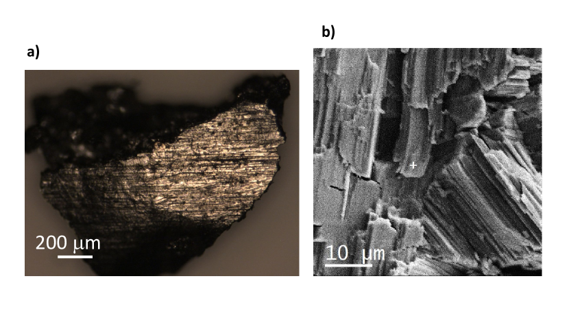
Raman experiments were undertaken in the same sample in the 10 K – 300 K temperature range, employing a Horiba T64000 triple grating spectrometer and a dye laser of 594 nm excitation line. Spectra were acquired using a liquid nitrogen cooled CCD detector. The spectral resolution was better than 1 cm-1, as determined from a Gaussian fit of the spectrum of Ne lines. Power was kept below 1 mW to avoid a temperature-induced phase transformation by laser heating [24]. The sample, displayed in Fig. 1(a), was kept in a liquid He flow cryostat during the experiment and temperature was read using a PT100 sensor.
II.3 Ab initio calculations
Ab initio zero-temperature total-energy simulations were carried out within the framework of density functional theory, DFT [25], as implemented in the Vienna ab initio Simulation Package [26], VASP, using the projector augmented-wave (PAW) pseudopotentials [27, 28]. A plane-wave energy cutoff of 380 eV was employed to ensure accurate converged results. The k-point sampling of the Brillouin zone, BZ, was performed using a 6146 dense grid to ensure high convergence in the integration over the BZ. Exchange-correlation energy was described using the generalized gradient approximation, GGA, with the Perdew-Burke-Ernzerhof (PBE) functional [29] including the dispersive corrections using the Grimme DFT-D3 method [30]. Spin-orbit coupling was taken into account in the band structure calculations, which were obtained with and without including this term. The high symmetry path was chosen using the SeeK-path utility [31]. The unit cell parameters and the atomic positions were fully relaxed imposing that the forces on the atoms were less than 0.003 eV/Å, and the deviations of the stress tensors from a diagonal hydrostatic form were lower than 0.1 GPa. These conditions resulted in Å, Å, and Å, in good agreement with the experimental values reported in the literature, e.g., by Ref. [32], of 11.71, 4.11, and 11.43 Å, respectively.
Lattice-dynamic calculations of the phonon modes were carried out at the zone centre ( point) of the BZ with the Phonopy package [33]. These calculations provide not only the frequency of the normal modes, but also their symmetry and their polarization vectors. This allows us to identify the irreducible representations and the character of the phonon modes at the point. A 444 supercell was used in order to obtain the phonon dispersion, and the phonon density of states.
III Results
Figure 1 displays the (a) optical and (b) SEM images of the o-Bi2Se3 sample employed in this study. A stratified structure is observed at the microscale, with - planes piled on top of each other. The sample has a shiny metalic-like luster that already indicates an electronic band gap of energies below the visible range. The cross on Fig. 1(b) indicates the region where CL spectra were acquired.
III.1 Electronic bandstructure and bandgap
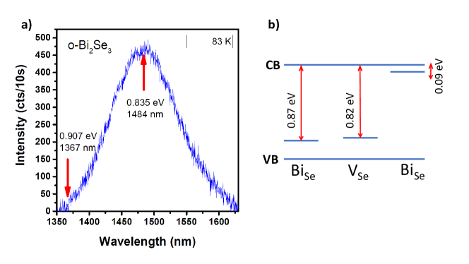
The CL spectrum taken at 83 K is shown in Fig. 2(a), revealing a broad band peaked at 1484 nm (0.835 eV) and a higher energy edge at 1367 nm (0.907 eV). Since a direct bandgap is expected, the peak value can be considered a lower limit of the electronic band gap energy, that we assume to stem from defect levels. Optical absorption experiments using near infrared light on Pnma Bi2Se3 obtained by electrodeposition reveal a bandgap varying between 0.9 eV for 0.5 m thick films to 1.25 eV for the thickest films, suggesting their potential for photovoltaic applications [32]. Our estimate for the bandgap is consistent with this range. In order to shed more light to the nature of this CL band, we calculated the electronic band structure of o-Bi2Se3. This is displayed in Fig. 2(c) along the main symmetry directions of the BZ, indicating with red solid and black dashed lines the electronic bands obtained with and without including SOC effects, respectively. As a general trend, taking into account SOC effects results into lower conduction band energies and a narrowing of the band gap. These calculations predict an indirect nature of the band gap, located between a maximum of the valence band (VB) along the -Z direction and a minimum of the conduction band (CB) along the -Y direction. Table 1 displays the values of the calculated direct and indirect electronic band gap of orthorhombic Bi2Se3 with and without including SOC effects. For the sake of completeness, our data are compared with those stemming from similar DFT and GW calculations [34, 35, 36]. The indirect nature of the band gap revealed by our calculations, both with and without SOC, is in agreement with predictions made by Ref. [36]. The calculated band gap energy difference between direct and indirect gaps, however, amounts to 0.1-0.2 eV, which makes it challenging to ascertain the true nature of the gap. Variations on the lattice parameters results in significant changes in the calculated band gap [36], e.g., up to 0.3 eV, between the values obtained using the experimental lattice constants and those corresponding to DFT fully optimized ones. This fact also prevents the determination of the direct or indirect nature of the band gap based solely on the calculated data.
Cathodoluminescence data, however, show a very weak signal at low temperature. This signal quickly vanishes with increasing temperature to 90 K. This makes us attribute the band gap to indirect transitions from the VB to the CB. Tumelero et al. [17] reported a calculated band gap of 1.2 eV and a comprehensive DFT study of the main defect energy levels on o-Bi2Se3, finding donor-type defect levels at 0.84 eV and 0.82 eV from the bottom of the CB corresponding to BiSe antisite and Se vacancies, respectively. These levels are in agreement with the peak energy of the CL spectrum, located at 0.835 eV. Figure 2(b) displays a schematic diagram of the potential transitions between these defect bands and both the VB and the CB to illustrate the possible origin of the features in the CL spectrum. Assuming a bandgap of 0.91 eV according the most accurate GW calculations with SOC effects [36], an alternative explanation for this peak would be a transition from acceptor states linked to a BiSe antisite, of 0.09 eV calculated activation energy [17]. This scenario matches as well with the peak energy of detected CL signal, 0.835 eV, that can be taken as an experimental low energy estimate for the electronic bandgap.
III.2 Raman phonon frequencies at low temperature
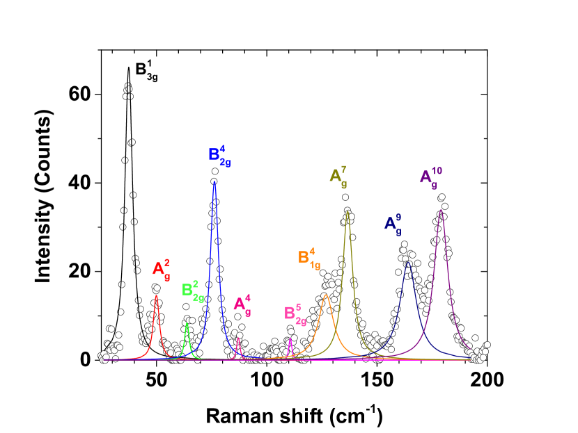
Figure 3 shows the Raman spectrum of Pnma Bi2Se3 obtained at 10 K. Several peaks appear in the spectrum and are attributed to different modes, the symmetry indicated in the figure. The highest energy mode peaks at about 170 cm-1. To the best of our knowledge, only one work has previously reported the o-Bi2Se3 Raman spectra recently for temperatures between 300 K and 570 K [37]. However, anharmonic effects are expected to be significant at those temperatures given the relatively low energy of the o-Bi2Se3 phonon modes. A precise determination of these anharmonic effects requires therefore to investigate the temperature dependence of the Raman spectra from 10 K up to room temperature and above.
III.3 Temperature dependence of the Raman spectrum
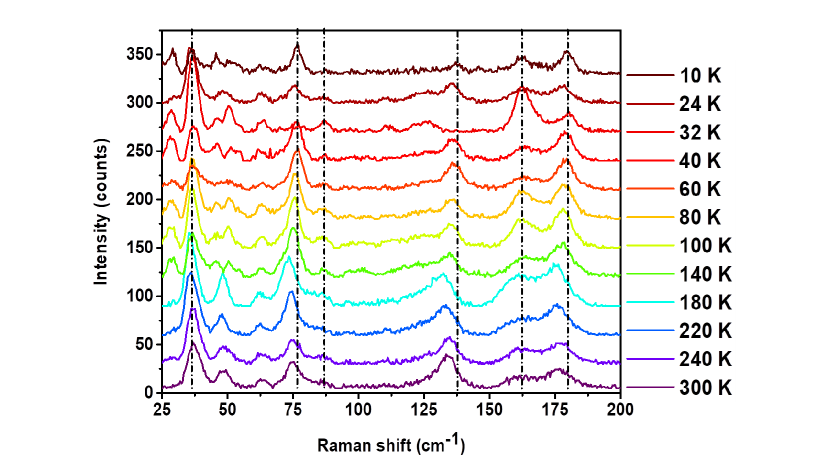
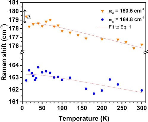
Figure 4(a) plots the Raman spectra at selected values in this 10-300 K temperature range. Some general trends are apparent: i) Phonon frequencies shift towards lower values with increasing temperature, as expected from the activation of third and high-order anharmonic decay channels, ii) this shift is larger for higher frequency modes, and iii) Raman peaks broaden and Raman intensities tend to decrease with increasing temperature, with a couple of exceptions, also in alignment with an increasing anharmonicity and thereby reduced phonon lifetime. Since the Raman spectra were taken in a polycrystalline sample, we attribute intensity fluctuations and appearance of additional peaks to changes in the laser spot position when the sample temperature is increased. A Voigt profile was used to fit the peaks in the Raman spectra, taking into account an experimental resolution of 1 cm-1. As anharmonic effects are typically more visible in the high energy modes, we display in Fig. 4(b) the Raman shift of the upper two modes as a function of temperature. This figure shows as well a fit to the experimental phonon frequencies with a two-oscillator model assuming anharmonic decay into two modes of equal energy , the so-called Klemens Ansatz [38], given by Eq. III.3:
where is the unrenormalized zero-temperature phonon energy, is the energy renormalization at 0 K, is the Bose-Einstein function, and and are Planck’s and Boltzmann’s constants, respectively. is a phonon frequency lower than and, since energy conservation does not hold for these transitions [39], it may be taken as an adjustable parameter. However, to simplify the number of fitted parameters, we have artificially imposed . Since ab initio phonon frequencies are usually obtained within the harmonic approximation, comparison between experimental and calculated Raman frequencies is more accurate and appropriate using the values obtained for , rather than the experimental values at low temperature. Understanding anharmonicity using ab initio simulations requires much more complex calculations similar to those reported in the pioneering work of Debernardi et al. in Ref. [40], and it is beyond the scope of this work.
In the high temperature limit, . From this limit together with Eq. III.3 we can calculate the slope of the temperature dependence of the Raman phonons at the high temperature range. Given the relatively low Raman frequencies of o-Bi2Se3, one can safely assume that at room temperature we are in this high regime, and then
| (2) |
IV Analysis
Pnma-type Bi2Se3 has an orthorhombic cell with 20 atoms per unit cell, thus yielding a rather complex map of phonon dispersion relations with 60 different phonon branches, similar to Sb2S3 and Sb2Se3 [41, 42]. Group theory predicts 60 vibrational modes at the Brillouin zone center whose irreducible representations are: , where B1g, B2g, B3g, and Ag modes correspond to Raman-active modes, B1u, B2u, and B3u modes correspond to infrared-active modes, Au modes are silent, and 1 B1u, 1 B2u and 1 B3u modes are acoustic modes. This leads to 30 Raman-active modes and 22 infrared-active modes.
The lattice dynamics of its trigonal counterpart, Rm Bi2Se3, is considerably simpler, as the crystal lattice has 5 atoms in the primitive unit cell. Therefore, only 15 vibrational modes appear at the zone center [43, 44]. The irreducible representations for the zone-center modes in this case are: , where A1g and Eg modes are Raman active, A2u and Eu modes are infrared active, Eu and Eg are doubly degenerated, and one A2u and one Eu modes correspond to the acoustic phonons. There are, hence, four Raman-active modes, and , that are observed at 39 cm-1 (), 71.5 cm-1 (), 132.5 cm-1 (), and 174 cm-1 () at room temperature and ambient pressure [43, 45, 46].
The Raman modes of trigonal Bi2Se3 have been subject of intense investigation since the pioneering work by Richter, Köhler, and Becker in 1977 [47], addressing both bulk single crystals [48, 49, 50], few epitaxial layers [51, 52, 53, 45], thin films [54] and nanoplates [55, 56]. Several studies report the temperature dependence of these modes at different temperature ranges [57, 55, 49, 46], and pressure [44] and magnetic field dependence [46] have also been investigated. The lattice dynamics of orthorhombic Pnma Bi2Se3, on the contrary, has only received attention very recently [37].
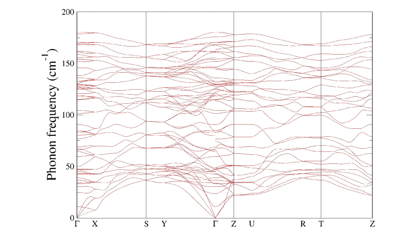
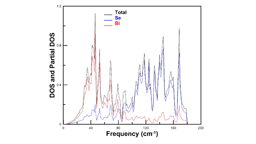
Figure 5(a) displays the calculated phonon dispersion relations along the main symmetry directions of o-Bi2Se3, whereas Fig. 5(b) shows the total, and Bi and Se projected partial one-phonon densities of states (DOS). As expected, the higher frequency modes are dominated by displacements of the Se sublattice. The Van-Hove singularities of the one-phonon DOS are expected to play a role in the peak broadening of the Raman spectra of alloys of o-Bi2Se3, as for example in thermoelectric materials such as in orthorhombic Bi2TexSe1-x, due to disorder-induced breakdown of momentum conservation.
From the 30 Raman-active modes, only around 10 modes can be identified due to both the presence of overlapping modes in the region up to 200 cm-1 within the spectral resolution and the polycrystalline character of the sample under investigation. A similar number of Raman-active modes were previously measured at room conditions in Pnma-type Sb2Se3 up to 250 cm-1 [41], in Pnma-type Bi2S3 up to 300 cm-1 [58], and in Pnma-type Sb2S3 up to 350 cm-1 [59, 42].
Table 2 displays the calculated Raman frequencies both with and without taking into account SOC effects, with the values of and derived from our experimental results, the Raman frequencies obtained at 300 K, and those reported in Ref. [37]. We also report here the high temperature limit of the temperature derivative of the Raman phonon frequencies, as calculated with Eq. 2. Another estimate for the temperature derivative at room temperature can be obtained by using the approximation . In this case, much lower values are obtained, e.g., for the highest frequency modes an average temperature derivative of and cm-1 K-1, similar to those reported for trigonal Bi2Se3 modes (between and cm-1 K-1) [60, 61, 55]. The values of give information about the zero-temperature renormalization of the phonon frequency, and are typically larger the more anharmonic the material. We observed in Table 2 that only the largest energy mode displays significant renormalization, the largest value being only slightly lower than those reported for CuI, a prototypical anharmonic semiconductor with similar Raman highest frequency [39].
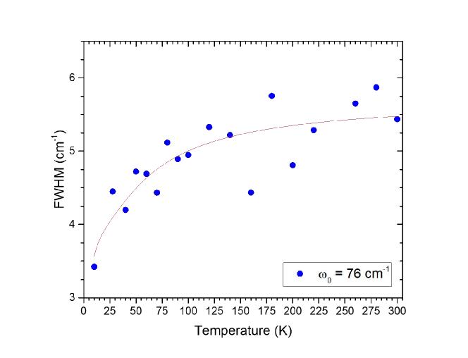
We can, therefore, conclude that the anharmonic effects are significant in this material. However, the anharmonicity seems to be lower than that exhibited by trigonal Bi2Se3 that presents both larger linewidths of the Raman peaks and an overshooting at 50 K of the higher A1g Raman frequency as a function of temperature, indicating phonon interactions with the electronic system beyond the expected anharmonic decay [46]. Unfortunately, for o-Bi2Se3 the large number of overlapping Raman modes in a relatively small energy range challenges a thorough analysis of the anharmonicity through direct investigation of the phonon linewidths as a function of temperature. Despite this overlap, we were able to evaluate the temperature dependence of the linewidth of two of the modes, corresponding to bare frequencies cm-1 and 180 cm-1, displayed in Fig. 6(a) and (b), respectively. In those figures a sudden increase in linewidth is observed below 100 K, followed by a more moderate increase at higher temperatures. This is an indication of the strong anharmonicity of this modification of Bi2Se3. In order to get a reasonable fit, we had to assume an anharmonic decay into two phonons of frequency and , following the energy conservation rules that hold strictly in the case of linewidths. The data were fitted using the equation [39]:
| (3) |
Values of cm-1 and 36(8) cm-1, and of cm-1 and 5.6(1) cm-1 were obtained from the fit for the Raman phonon frequencies cm-1 and 180 cm-1, respectively. Note that the linewidth values plotted in Fig. 6 have been obtained after deconvolution of the Raman peak with a Gaussian of 1 cm-1 corresponding to the spectral resolution, in a similar way as described in Ref. [46]. The higher value observed for the higher frequency mode indicates the larger anharmonic effects displayed by this mode, presumably due to the larger value of the two phonon density of states, since there is a critical point in the phonon bandstructure at both 36 cm-1 and 144 cm-1. An extremely rare two-slope behavior with a damping of the increase of the phonon linewidth is observed in the temperature dependence for both modes. This unexpected behavior contrasts to the nearly parabolic trend reported in Ref. [46] for the trigonal polytype, frequently observed in semiconductors. These damping is attributed to the combination of a very high frequency mode and a much lower frequency mode in the decay channels of the Raman modes.
V Conclusions
We have reported here the temperature dependence of the Raman spectrum of orthorhombic, Pnma, Bi2Se3 in the 10 K – 300 K temperature range, and analyzed the Raman shifts using a two-oscillator Klemens-like model. The Raman shifts at 10 K are in agreement with the predictions we obtained using linear-response ab initio calculations. An anomalous anharmonic behavior is observed in the temperature dependence of the phonon linewidths for at least two of the Raman modes, displaying a two-slope trend with increasing temperature. We have also observed by cathodoluminescence a lower limit of 0.835 eV for the electronic bandgap of o-Bi2Se3. This band gap seems to have an indirect nature, given the low intensity observed in the experimental data, and also in agreement with both our calculations and those previously reported using the GW approximation. These results shed light to some of the fundamental properties of orthorhombic Bi2Se3, a metastable material of interest for applications in thermoelectrics.
*
Appendix A Additional information on the temperature dependence of Raman phonon frequencies and the one-phonon DOS
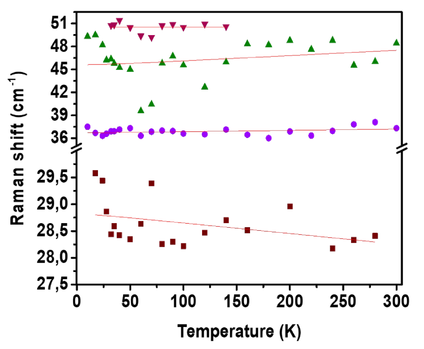
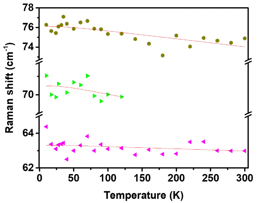
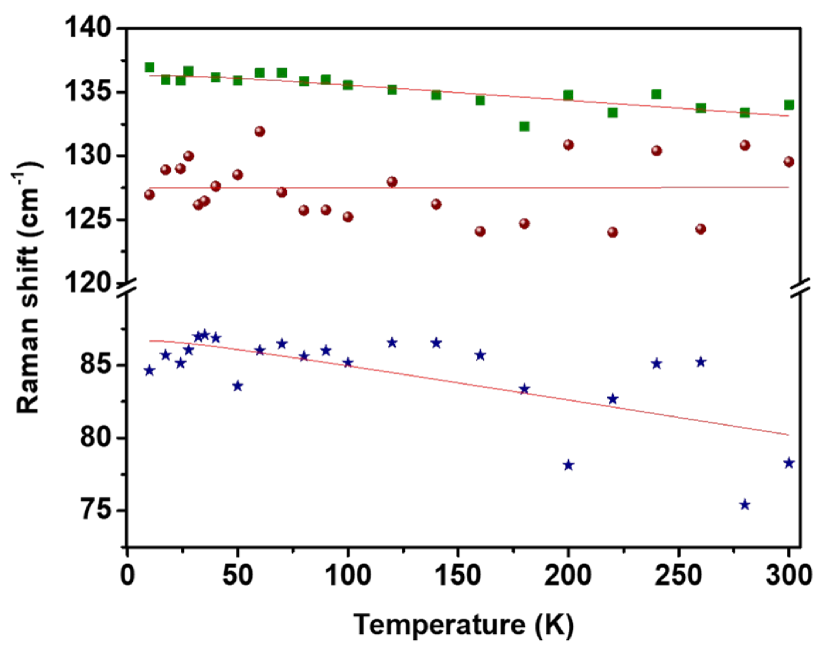
Figures 7, 8, and 9 display the temperature dependence of the Raman low frequency modes shown on Fig. 3.
Table 3 displays the assignments of the Van-Hove singularities of the calculated one-phonon DOS, useful to determine potential disorder activated features in the Raman spectra.
Acknowledgements.
This publication is financed by the Spanish Ministerio de Ciencia e Innovación and the Agencia Estatal de Investigación MCIN/AEI/10.13039/501100011033 as part of the project MALTA Consolider Team Network (RED2022-134388-T), and I+D+i projects PID2019-106383GB-42/43, PID2021-126046OB-C22, TED2021-130786B-I00 also funded by MTED, and PID2022-138076NB-C42/C44 co-financed by EU FEDER funds. This study is also funded by project PROMETEO CIPROM/2021/075 (GREENMAT), financed by the Generalitat Valenciana, and by Generalitat Valenciana through project MFA/2022/025 (ARCANGEL), and also forms part of the Advanced Materials programme supported by MCIN with funding from European Union NextGenerationEU (PRTR-C17.I1).References
- Zhang et al. [2009] H. Zhang, C.-X. Liu, X.-L. Qi, X. Dai, Z. Fang, and S.-C. Zhang, Nature Physics 5, 438 (2009).
- Hsieh et al. [2009] D. Hsieh, Y. Xia, D. Qian, L. Wray, J. Dil, F. Meier, J. Osterwalder, L. Patthey, J. Checkelsky, N. Ong, A. Fedorov, H. Lin, A. Bansil, D. Grauer, Y. Hor, R. Cava, and M. Hasan, Nature 460, 1101 (2009).
- Bianchi et al. [2010] M. Bianchi, D. Guan, S. Bao, J. Mi, B. Iversen, P. King, and P. Hofmann, Nature Communications 1, 128 (2010).
- Cheng et al. [2010] P. Cheng, C. Song, T. Zhang, Y. Zhang, Y. Wang, J.-F. Jia, J. Wang, Y. Wang, B.-F. Zhu, X. Chen, X. Ma, K. He, L. Wang, X. Dai, Z. Fang, X. Xie, X.-L. Qi, C.-X. Liu, S.-C. Zhang, and Q.-K. Xue, Phys. Rev. Lett. 105, 076801 (2010).
- Hor et al. [2010] Y. Hor, A. Williams, J. Checkelsky, P. Roushan, J. Seo, Q. Xu, H. Zandbergen, A. Yazdani, N. Ong, and R. Cava, Phys. Rev. Lett. 104, 057001 (2010).
- Peng et al. [2009] H. Peng, K. Lai, D. Kong, S. Meister, Y. Chen, X. Qi, S.-C. Zhang, Z. Shen, and Y. Cui, Nature Materials 9, 225 (2009).
- Li et al. [2014] C. Li, O. van ’t Erve, J. Robinson, Y. Liu, L. Li, and B. Jonker, Nature Nanotechnology 9, 218 (2014).
- Mellnik et al. [2014] A. Mellnik, J. Lee, A. Richardella, J. Grab, P. Mintun, M. Fischer, A. Vaezi, A. Manchon, E.-A. Kim, N. Samarth, and D. Ralph, Nature 511, 449 (2014).
- Katmis et al. [2016] F. Katmis, V. Lauter, F. Nogueira, B. Assaf, M. Jamer, P. Wei, B. Satpati, J. Freeland, I. Eremin, D. Heiman, P. Jarillo-Herrero, and J. Moodera, Nature 533, 513 (2016).
- Lin et al. [2018] Z. Lin, Y. Liu, U. Halim, M. Ding, Y. Liu, Y. Wang, C. Jia, P. Chen, X. Duan, C. Wang, F. Song, M. Li, C. Wan, Y. Huang, and X. Duan, Nature 562, 254 (2018).
- Mishra et al. [1997] S. Mishra, S. Satpathy, and O. Jepsen, J. Phys.: Condens. Matter 9, 461 (1997).
- Hor et al. [2009] Y. Hor, A. Richardella, P. Roushan, Y. Xia, , J. Checkelsky, A. Yazdani, M. Hasan, N. Ong, and R. Cava, Phys. Rev. B 79, 195208 (2009).
- Snyder and Toberer [2008] G. Snyder and E. Toberer, Nature Materials 7, 105 (2008).
- Fang et al. [2020] T. Fang, F. Li, Y. Wu, Q. Zhang, X. Zhao, and T. Zhu, Appl. Energy Mater. 3, 2070 (2020).
- Klösel et al. [2023] K. Klösel, C. Roman, and C. Hierold, J. Microelectromechanical Systems 32, 445 (2023).
- Cao and Wang [2013] T. Cao and S. Wang, Nanoscale Res. Lett. 8, 526 (2013).
- Tumelero et al. [2016a] M. Tumelero, R. Faccio, and A. Pasa, J. Phys. Chem. C 120, 1390 (2016a).
- Earley [1950] J. W. Earley, Am. Mineral. 35, 337 (1950).
- Schönherr et al. [2015] P. Schönherr, S. Zhang, Y. Liu, P. Kusch, S. Reich, T. Giles, D. Daisenberger, D. Prabhakaran, Y. Chen, and T. Hesjedal, Phys. Status Solidi RRL 9, 130 (2015).
- Atabaeva et al. [1973] E. Y. Atabaeva, C. Mashkov, and S. Popova, Kristallografiya 18, 173 (1973).
- Kang et al. [2017] Y. Kang, Q. Zhang, C. Fan, W. Hu, C. Chen, L. Zhang, F. Yu, Y. Tian, and B. Xu, J. Alloys and Compounds 700, 223 (2017).
- Xiao et al. [2009] C. Xiao, J. Yang, W. Zhu, J. Peng, and J. Zhang, Electrochimica Acta 54, 6821 (2009).
- Serebryanaya et al. [2020] N. Serebryanaya, R. Bagramov, S. Buga, I. Pahomov, N. Eliseev, and V. Blank, Phys. Stat. Sol. B 257, 2000145 (2020).
- Manjón et al. [2021] F. Manjón, S. Gallego-Parra, P. Rodríguez-Hernández, A. Muñoz, C. Drasar, V. Muñoz-Sanjosé, and O. Oeckler, J. Mat. Chem. C 9, 6277 (2021).
- Hohenberg and Kohn [1964] P. Hohenberg and W. Kohn, Phys. Rev. 136, B864 (1964).
- Kresse and Fürthmuller [1996] G. Kresse and J. Fürthmuller, Phys. Rev. B 54, 11169 (1996).
- Blochl [1994] P. Blochl, Phys. Rev. B 50, 17953 (1994).
- Kresse and Joubert [1999] G. Kresse and D. Joubert, Phys. Rev. B 59, 1758 (1999).
- Perdew et al. [1998] J. P. Perdew, K. Burke, and M. Ernzerhof, Phys. Rev. Lett. 77, 3865 (1998).
- Grimme et al. [2010] S. Grimme, J. Antony, S. Ehrlich, and S. Krieg, J. Chem. Phys. 132, 154104 (2010).
- Hinuma et al. [2017] Y. Hinuma, G. Pizzi, Y. Kumagai, F. Oba, and I. Tanaka, Comp. Mat. Sci. 128, 140 (2017).
- Tumelero et al. [2016b] M. Tumelero, L. Benetti, E. Isoppo, R. Faccio, G. Zangani, and A. Pasa, J. Phys. Chem. C 120, 11797 (2016b).
- Togo and Tanaka [2015] A. Togo and I. Tanaka, Scr. Mater. 108, 1 (2015).
- Caracas and Gonze [2005] R. Caracas and X. Gonze, Phys. Chem. Minerals 32, 295 (2005).
- Sharma and Srivastava [2010] Y. Sharma and P. Srivastava, AIP Conf. Proc. 1249, 183 (2010).
- Filip et al. [2013] M. Filip, C. Patrick, and F. Giustino, Phys. Rev. B 87, 205125 (2013).
- Souza et al. [2023] P. Souza, M. Tumelero, R. Faccio, R. Ahmed, C. P. Cid, G. Zangari, and A. Pasa, Phys. Chem. Chem. Phys. 25, 14440 (2023).
- Klemens [1966] P. Klemens, Phys. Rev. 148, 845 (1966).
- Serrano et al. [2012] J. Serrano, M. Cardona, T. M. Ritter, B. A. Weinstein, A. Rubio, and C. T. Lin, Phys. Rev. B 66, 245202 (2012).
- Debernardi et al. [1995] A. Debernardi, S. Baroni, and E. Molinari, Phys. Rev. Lett. 75, 1819 (1995).
- Fleck et al. [2020] N. Fleck, T. Hobson, C. Savory, J. Buckeridge, T. Veal, M. Correia, D. Scanlon, K. Durose, and F. Jäckel, J. Phys. Chem. A 8, 8337 (2020).
- Ibañez et al. [2016] J. Ibañez, J. Sans, C. Popescu, J. López-Vidrier, J. Elvira-Betanzos, V. Cuenca-Gotor, O. Gomis, F. Manjón, P. Rodríguez-Hernández, , and A. Muñoz, J. Phys. Chem. C 120, 10547 (2016).
- Vilaplana et al. [2011] R. Vilaplana, D. Santamaría-Pérez, O. Gomis, F. Manjón, J. González, A. Segura, A. Muñoz, P. Rodríguez-Hernández, E. Pérez-González, V. Marín-Borrás, V. Muñoz-Sanjosé, C. Drasar, and V. Kucek, Phys. Rev. B 84, 184110 (2011).
- Deshpande et al. [2014] M. Deshpande, S. Bhatt, V. Sathe, R. Rao, and S. Chaki, Physica B 433, 72 (2014).
- Eddrief et al. [2014] M. Eddrief, P. Atkinson, V. Etgens, and B. Jusserand, Nanotechnology 25, 245701 (2014).
- Buchenau et al. [2020] S. Buchenau, S. Scheitz, A. Sethi, J. Slimak, T. Glier, P. Das, T. Dankwort, L. Akinsinde, L. Kienle, A. Rusydi, C. Ulrich, S. Cooper, and M. Rübhausen, Phys. Rev. B 101, 245431 (2020).
- Richter et al. [1977] W. Richter, H. Köhler, and C. Becker, Phys. Stat. Sol. B 84, 619 (1977).
- Zhang et al. [2011] J. Zhang, Z. Peng, A. Soni, Y. Zhao, Y. Xiong, B. Peng, J. Wang, M. Dresselhaus, and Q. Xiong, Nano Lett. 11, 2407 (2011).
- Gnezdilov et al. [2011] V. Gnezdilov, Y. Pashkevich, H. Berger, K. Conder, and P. Lemmens, Phys. Rev. B 84, 195118 (2011).
- Sharma et al. [2021] D. Sharma, M. Sharma, R. Meena, and V. Awana, Physica B 600, 412492 (2021).
- Shahil et al. [2012] K. Shahil, M. Hossain, V. Goyal, and A. Balandin, J. Appl. Phys. 111, 054305 (2012).
- Zhao et al. [2014] Y. Zhao, X. Luo, J. Zhang, J. Wu, X. Bai, M. Wang, J. Jia, H. Peng, Z. Liu, S. Quek, and Q. Xiong, Phys. Rev. B 90, 245428 (2014).
- Humlícek et al. [2014] J. Humlícek, D. Hemzal, A. Dubroka, O. Caha, H. Steiner, G. Bauer, and G. Springholz, Phys. Scr. T162, 014007 (2014).
- Niherysh et al. [2021] K. Niherysh, J. Andzane, M. Mikhalik, S. Zavadsky, P. Dobrokhotov, F. Lombardi, S. Prischepa, I. Komissarov, and D. Erts, Nanoscale Adv. 3, 6395 (2021).
- Zhou et al. [2018] F. Zhou, Y. Zhao, W. Zhou, and D. Tang, Appl. Sci. 8, 1794 (2018).
- Kondo et al. [2023] T. Kondo, T. Nozaki, R. Kotabe, and Y. Terai, Jpn. J. Appl. Phys. 62, SD1016 (2023).
- Irfan et al. [2014] B. Irfan, S. Sahoo, A. Gaur, M. Ahmadi, M.-F. Guinel, R. Katiyar, and R. Chatterjee, J. Appl. Phys. 115, 173506 (2014).
- Zhao et al. [2011] Y. Zhao, K. Chua, C. Gan, J. Zhang, B. Peng, Z. Peng, , and Q. Xiong, Phys. Rev. B 84, 205330 (2011).
- Sereni et al. [2010] P. Sereni, M. Musso, P. Knoll, P. Blaha, K. Schwarz, and G. Schmidt, AIP Conf. Proc. 1267, 1131 (2010).
- Kim et al. [2012] Y. Kim, X. Chen, Z. Wang, J. Shi, I. Miotkowski, Y. Chen, P. Sharma, A. Sharma, M. Hekmaty, Z. Jiang, and D. Smirnov, Appl. Phys. Lett. 100, 071907 (2012).
- Yang et al. [2012] X. Yang, Z. Zhou, Y. Wang, R. Jiang, W. Zheng, and C. Sun, J. Appl. Phys. 112, 083508 (2012).
| Direct gap | Indirect gap | |
| Exp. (CL data) | 835(10) | |
| Without SOC | 974 | 948 |
| With SOC | 624 | 601 |
| Other DFT | 900a, 1100b, 990c | 860c |
| GW with SOC | 910c |
| Mode | Symmetry | Theory, | Experiment | Ref. [37] | ||||
| With SO | No SO | (300 K) | () | (300 K) | ||||
| 1 | B | |||||||
| 2 | B | |||||||
| 3 | A | |||||||
| 4 | B | |||||||
| 5 | B | |||||||
| 6 | B | |||||||
| 7 | A | |||||||
| 8 | A | |||||||
| 9 | B | |||||||
| 10 | B | |||||||
| 11 | B | |||||||
| 12 | A | |||||||
| 13 | B | |||||||
| 14 | B | |||||||
| 15 | B | 109.0 | ||||||
| 16 | A | |||||||
| 17 | A | |||||||
| 18 | B | |||||||
| 19 | B | |||||||
| 20 | B | 126.6 | ||||||
| 21 | A | |||||||
| 22 | B | |||||||
| 23 | B | |||||||
| 24 | B | 141.1 | ||||||
| 25 | B | |||||||
| 26 | A | |||||||
| 27 | A | 158.7 | ||||||
| 28 | B | |||||||
| 29 | A | 173.0 | ||||||
| 30 | B | |||||||
| DOS | Assignment | DOS | Assignment | ||
| (cm-1) | (cm-1) | ||||
| 31 | 0.40 | X | 111 | 0.61 | SY,RT |
| 35 | 0.58 | X,ZU | 118 | 0.72 | RT |
| 43 | 0.80 | RT | 124 | 0.67 | UR |
| 46 | 1.13 | X,SY | 132 | 0.60 | ZUR |
| 53 | 0.77 | UR | 143 | 0.73 | Z |
| 68 | 0.65 | SY | 145 | 0.89 | Y |
| 79 | 0.41 | SY,ZU | 156 | 0.54 | X |
| 90 | 0.34 | SY,Z | 160 | 0.48 | Z |
| 100 | 0.28 | RT | 169 | 0.98 | X |
| 107 | 0.41 | ZU | 178 | 0.17 | X |