Terahertz ratchet in graphene 2D metamaterial
formed by a patterned gate with an antidot array
Abstract
We report the observation of the terahertz-induced ratchet effect in graphene-based two-dimensional (2D) metamaterials. The metamaterial consists of a graphite gate patterned with an array of triangular antidots placed under a graphene monolayer. We show that the ratchet current appears due to the noncentrosymmetry of the periodic structure unit cell. The ratchet current is generated owing to the combined action of a spatially periodic in-plane electrostatic potential and a periodically modulated radiation electric field caused by near-field diffraction. The magnitude and direction of the ratchet current are shown to be controlled by voltages applied to both back and patterned gates, which change the lateral asymmetry, carrier type and density. The phenomenological and microscopic theories of ratchet effects in graphene-based 2D metamaterials are developed. The experimental data are discussed in the light of the theory based on the solution of the Boltzmann kinetic equation and the calculated electrostatic potential profile. The theory describes well all the experimental results and shows that the observed ratchet current consists of the Seebeck thermoratchet contribution as well as the linear contribution, which is sensitive to the orientation of the radiation electric field vector with respect to the triangles.
I Introduction
Recently, DC currents excited by terahertz (THz) radiation in two-dimensional systems with lateral 1D gratings whose period is much smaller than the radiation wavelength have attracted increasing attention [1, 2, 3, 4, 5, 6, 7, 8, 9, 10, 11, 12, 13, 14, 15, 16, 17, 18, 19]. These studies explored a number of fascinating effects and paved the way for the development of fast room-temperature THz detectors [5, 7, 9, 12, 15, 18, 20]. A particularly promising system discussed so far is the comb-like dual-grating-gate (DGG) graphene-based field-effect transistor structures [2, 4, 5, 6, 7, 8, 9, 10, 11, 12, 13, 14, 15, 16, 17, 18, 19]. In general, the generation of a DC current in lateral 1D periodic systems due to the action of an AC electric field requires two ingredients, namely an asymmetry of the periodic potential acting on the electrons and an asymmetric amplitude of the near-field , where is the modulation direction. The net DC electric current is proportional to the asymmetry parameter , where the overline stands for the average over the ratchet period [2, 4]. The conversion of the alternating electric field into direct current in the periodically modulated structures with broken spatial symmetry belongs to the class of ratchet effects, which are relevant in different fields of physics, chemistry and biology, for reviews see, e.g., [21, 22, 23, 24, 25, 26, 27, 28, 29, 30, 31]. Experiments carried out in DGG structures formed by periodically repeated metal stripes of two widths deposited on various low-dimensional electronic systems, such as semiconductor quantum wells or graphene, have revealed several microscopic mechanisms of the rectified current, namely electronic ratchet effects [1, 26, 32, 33, 2, 34, 10, 13, 16, 20], plasmonic ratchet/drag effects [35, 36, 37, 38, 39, 5, 40, 41, 7, 42, 9, 43, 44, 45, 10, 46, 47, 48, 49, 15, 50, 51, 16, 52, 18, 20], and the photothermoelectric effect [18, 53, 54, 55, 56, 57]. The ratchet effect has also been demonstrated for a periodic semicircular antidot array in Si/SiGe and AlGaAs/GaAs heterostructures excited by microwave radiation at frequencies of tens of GHz [58, 59] and has been proposed for energy-free microwave-based signal communication [34].
Here, we demonstrate that the ratchet effect can also be effectively generated by applying THz radiation to two-dimensional (2D) metamaterials formed by a patterned gate with an array of triangular shaped antidots placed under a graphene layer and having a period , where is the radiation wavelength. Microscopically, electrons feel the low symmetry of the system through the inhomogeneous near-field formed by radiation diffraction from the boundaries of the triangular antidots. The radiation electric field due to near-field diffraction is periodically modulated in 2D space with period . Another field acting on the electrons is due to the periodic asymmetric potential with barriers at the boundaries of the antidots. The 2D modulation of both fields leads to the lateral asymmetry vector parameter given by
| (1) |
where the overline denotes averaging over the 2D period. Although both the near-field intensity and the periodic potential are zero on average, the lateral asymmetry parameter is finite due to the low symmetry of the structure. It is clear that vanishes if both profiles of and have identical coordinate dependence. However, the near-field profile is different from that of the triangles, and therefore the parameter becomes nonzero. Applying linearly polarized THz radiation to unbiased structures, we obtained DC electric currents consisting of several contributions including the polarization-independent Seebeck thermoratchet current and the linear ratchet current, which is sensitive to the orientation of the driving radiation electric field with respect to the triangles. The asymmetric electrostatic potential in such structures can be efficiently varied by gate voltages applied to the patterned gate and/or by the uniform back gate voltages, allowing us to change the magnitude and the sign of the ratchet current in a controllable manner. The results are analyzed in terms of the phenomenological and microscopic theory of ratchet effects in periodic structures solving the Boltzmann kinetic equation. The experimental data and the theoretical results are discussed taking into account the calculated potential profile obtained from the electrostatic simulation using FEniCS [60] based on the finite element method.
II Sample and methods
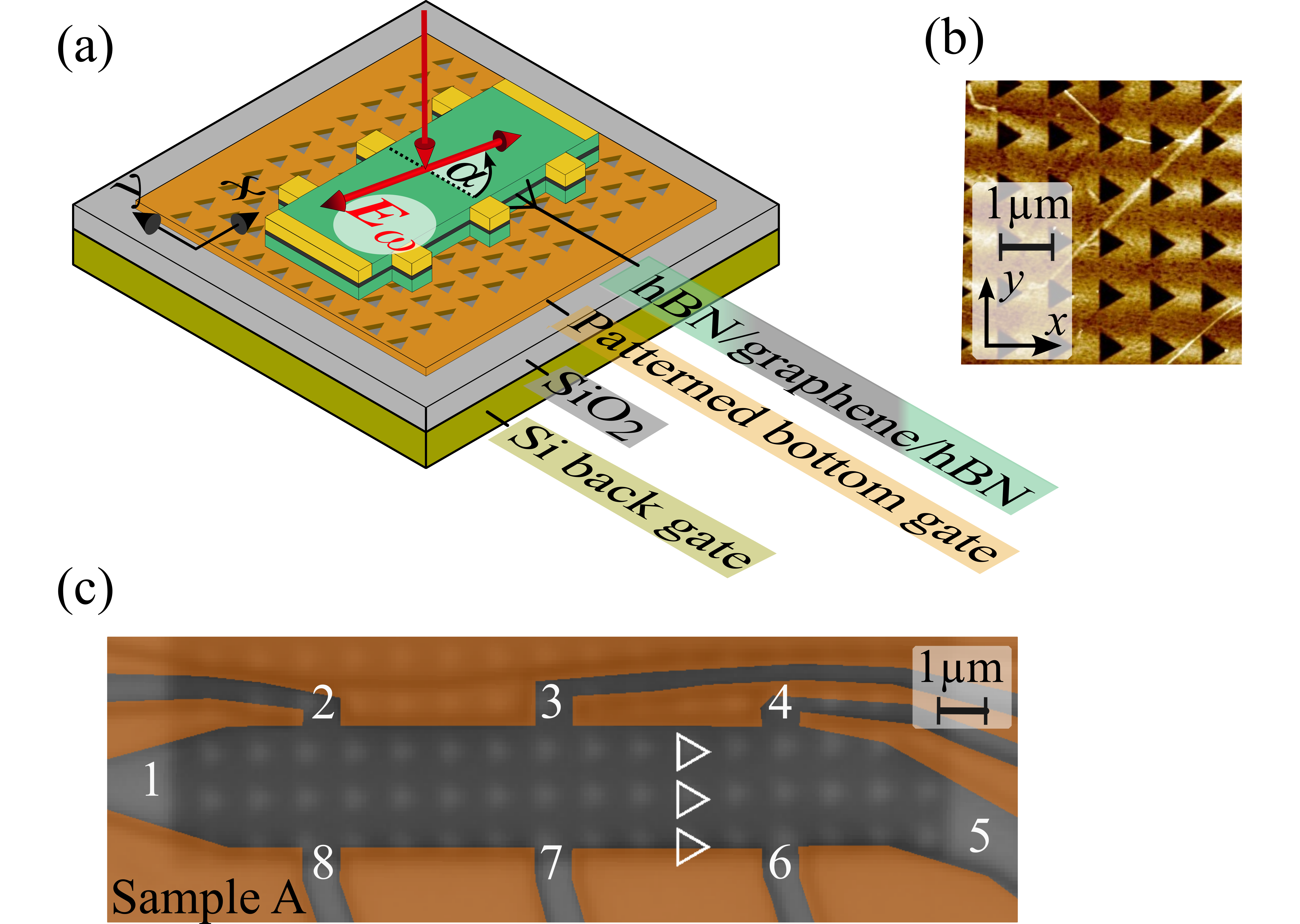
We fabricated our samples on a strongly -doped silicon chip, which operates as a conventional global back gate. The Si back gate is separated from the rest of the sample by a thick silicon dioxide, as shown in Fig. 1(a). On top of the insulator, we deposited the key element of the structure: a patterned bottom gate made of five layers graphene, which has equilateral triangular antidots with a side length of 0.6 m arranged in a square lattice with a period of 1 m, see Fig. 1(b). The lattice was fabricated by electron beam lithography and reactive ion etching using oxygen plasma. Monolayer graphene encapsulated in two layers of hexagonal boron nitride (hBN) was placed on top of the lattice. The lower and upper hBN layers in sample A (B) had thicknesses of about () and (), respectively. Using reactive ion etching, the samples were shaped into a Hall bar configuration, which for sample A (B) is () long and () wide, and were provided with ohmic chromium-gold contacts, see Fig. 1(a) and (c). The Hall resistance was measured as a function of the patterned gate , ranging from to at fixed magnetic fields ( T), not shown. According to , the maximum charge densities are cm-2 for electrons and cm-2 for holes, for further details, see Appendix A. The maximum carrier mobility for electrons and holes are cm2/Vs and cm2/Vs, respectively.
Figure 1(a) sketches the experimental setup. The ratchet current was excited applying normally incident linearly polarized THz radiation from an optically pumped far-infrared molecular gas laser operating at frequency (corresponding wavelength and photon energy ). The radiation was modulated by an optical chopper with frequency 130 Hz. The radiation power at the sample was about . The beam spot profile was measured by a pyroelectric camera [61] and had a Gaussian-like shape with a full width at half maximum of . Consequently, the sample was exposed to the power , where and are the areas of the sample and the laser beam, respectively. To extract and study different roots of the ratchet current, the radiation electric field vector was rotated in the sample plane using lambda-half quartz wave plates. The orientation of the vector was defined by the azimuth angle counted from the -axis, see Fig. 1(a).
The samples were placed in a vacuum chamber with a -cut crystal quartz window. To avoid illumination of the sample by visible and near-infrared light, the windows were covered by a black polyethylene film. All experiments were performed at room temperature. The generated photovoltage in the unbiased sample was amplified by a factor 100 and measured with standard lock-in technique. The voltage has been picked up from the contact pair 5-1 and has been picked up from contacts 8-2, with contacts 1 and 2 being grounded, respectively. The generated ratchet current density was calculated as , where is the two-point sample resistance, is the input impedance of the amplifier, and is the Hall bar width.
III Results
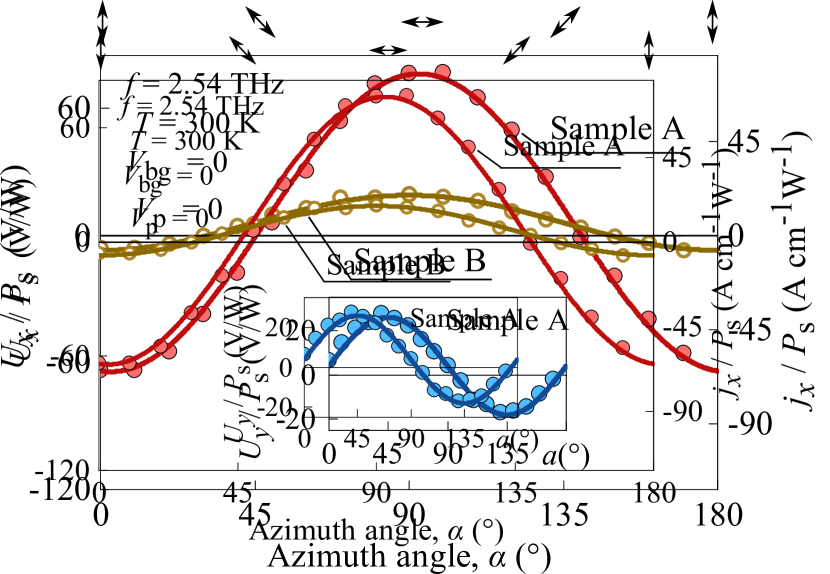
By irradiating the structures with the THz beam, we observed a polarization-dependent photocurrent. Figure 2 shows the photocurrent density normalized to the radiation power, , and the corresponding photovoltage , as a function of the angle , assigning the direction of the radiation electric field vector with respect to the height of the triangular antidots, see Fig. 1(a). The data are obtained in two graphene structures for zero back and patterned gate voltages in the directions along the triangle height () and base (). For this particular sequence of gate voltages, the polarization dependence of the signal is given by
| (2) | ||||
| (3) |
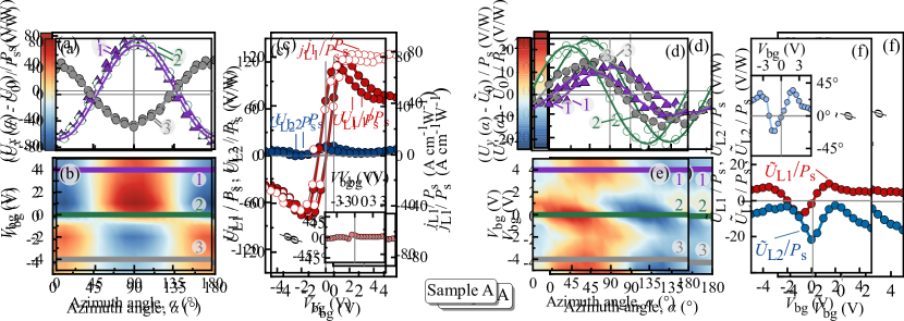
The application of the gate voltages changes the -dependence resulting in additional polarization-dependent and polarization-independent contributions. This is exemplarily shown in Figs. 3(a)–(f) for sample A at zero patterned gate voltage and various values of the back gate voltage. These plots reveal that the signals in - and -directions follow
| (4) | ||||
| (5) |
with coefficients being dependent on the gate voltages and . In particular, the polarization-dependent photovoltage detected in the -direction is formed by the interplay of two contributions having comparable amplitudes, and being characterized by different dependencies on the back gate voltage, see Fig. 3(f). This interplay leads to the gate-dependent phase shift in the -dependencies of described by
| (6) |
see Figs. 3(d)–(f). The back gate dependence of the phase shift is shown in the inset in Fig. 3(f). The polarization dependence of the photocurrent detected in -direction is less affected by the gate voltages. Figures 3(a) and (b) show that for most back gate voltages the photovoltage contribution is substantially higher than the one [see Fig. 3(c)], and the phase shift in the polarization dependence defined as
| (7) |
remains close to zero, see Fig. 3(b) and inset in Fig. 3(c). Note that a substantial deviation of the phase from zero is detected at high negative and simultaneously high positive only, see Fig. 6 (a).
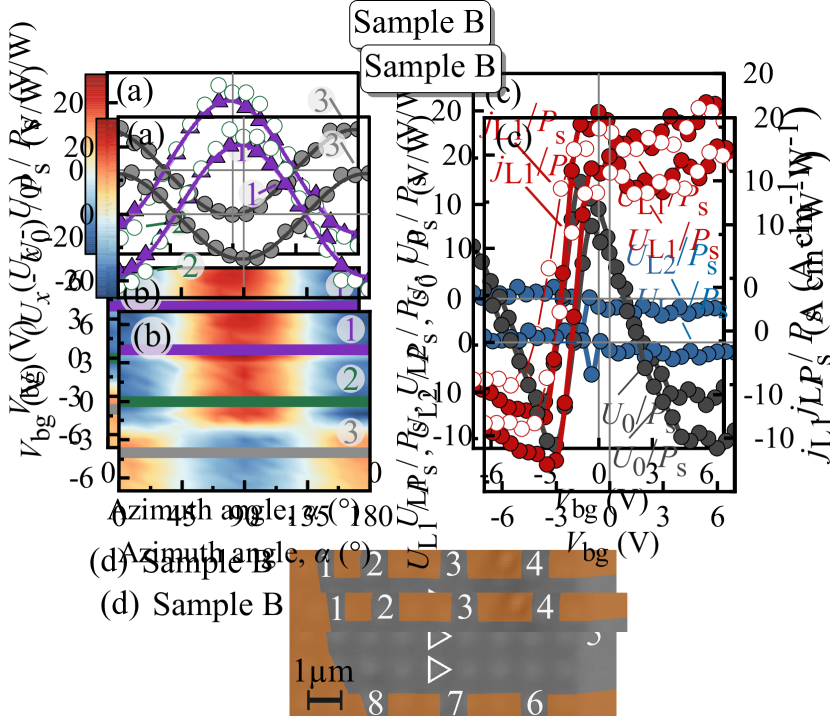
In the following, we focus on the data obtained in sample A for the -direction. Since , we present below a functional behavior of the and amplitudes only. Note that some data for the -direction and for sample B are given in Appendix B.
As addressed in the introduction, ratchet effects are highly sensitive to the degree of lateral asymmetry described by the parameter [see Eq. (1)], which is primarily caused by the asymmetry of the electrostatic potential. Consequently, back and patterned gate voltages should substantially change the ratchet current. Figures 4–6 show the variation of the and photovoltages as the back gate and/or the patterned gate voltage is varied. All plots were obtained by holding one of the gate voltages constant and varying the other.
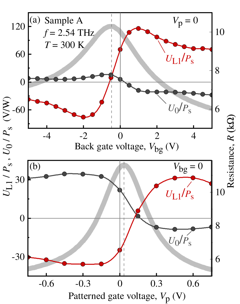
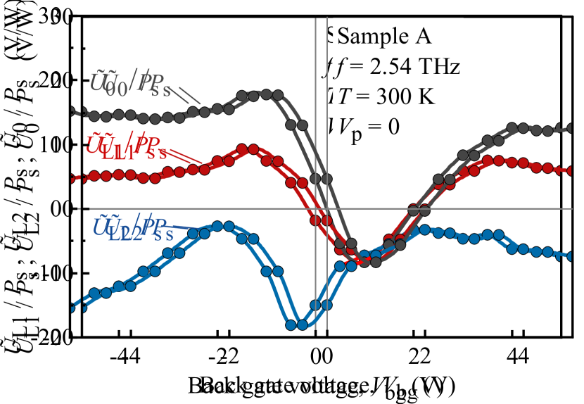
Figure 4 shows the back gate [panel (a)] and patterned gate [panel (b)] dependencies obtained for zero and , respectively. The figures reveal that the polarization-dependent and polarization-independent contributions behave similarly upon variation of both gate voltages: they change their sign near the resistance maximum, and they decrease only slightly with or at high gate voltages. Note that at high gate voltage amplitudes the sample resistance decreases, and consequently the corresponding ratchet currents, calculated as , increase slightly with increasing or . Figure 4 also demonstrates that for most gate voltage sequences the and contributions have opposite signs. Note that the contribution is less than 10 % of for all gate voltages except of those at which . Therefore is not shown in the plot.
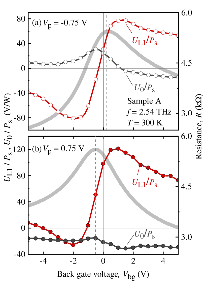
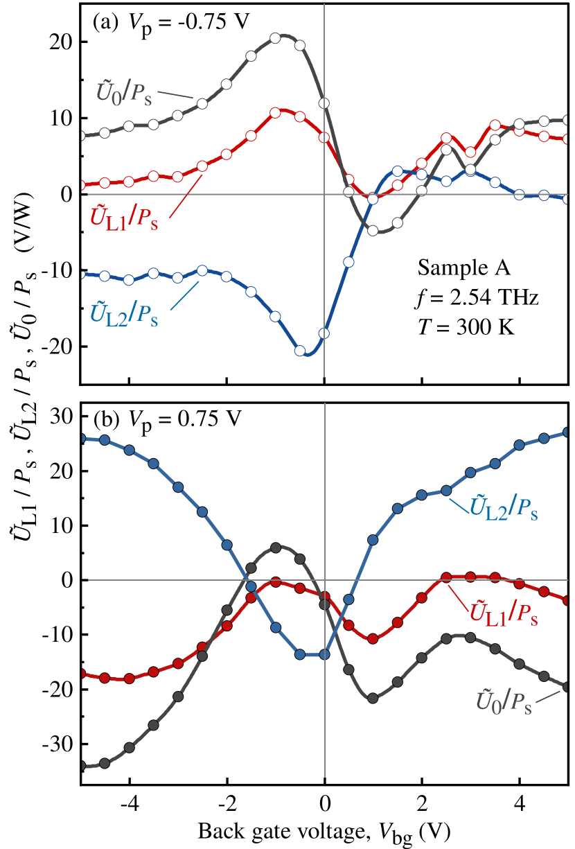
Figure 5(a) and (b) show the back gate voltage dependence of obtained for fixed positive ( V) and negative ( V) voltages applied to the patterned gate. It can be seen that the change of the patterned gate voltage polarity does not significantly modify the photosignal: in both plots dominates the photoresponse, reverses its sign in the vicinity of the resistance maximum and depends slightly on at high back gate voltages. Note that for positive patterned gate voltages, in contrast, at high negative back gate voltages the amplitude decreases and for V even changes its sign at V. For V the polarization-independent photoresponse is negative for all back gate voltages.
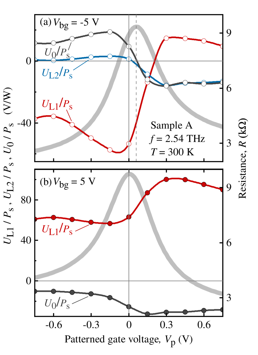
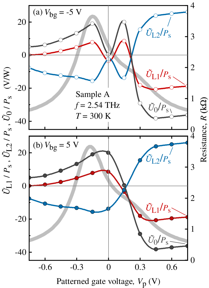
Figures 6(a) and (b) present the patterned gate voltage dependence obtained for large back gate voltages with opposite polarities of V and 5 V, respectively. Also under these conditions, the contribution dominates the photoresponse for nearly all gate voltages except for V at which all three contributions , , and have comparable amplitudes, see Fig. 6(a). While at negative back gate voltage the signals change their sign in the vicinity of the resistance maximum, at positive V both and keep their signs, see Fig. 6(b). At the same time, the magnitude of these contributions changes significantly in the gate voltage range where the structure resistance approaches its maximum value. Again, a reduction of the resistance increases the current magnitudes at high gate voltage amplitudes.
IV Discussion
To analyse the data obtained, we first present a symmetry analysis and microscopic theoretical treatment. In the presence of a substrate, a uniform gate, or adatoms deposited on one side of the sample, the symmetry of graphene is reduced to the non-centrosymmetric group C6v, because the equivalence of the and directions is removed. Even for this symmetry class, the generation of direct current under normal incidence radiation is forbidden, and indeed not observed, for a review see [62]. In general, normal incident radiation can give rise to edge photocurrents, which can be detected by measuring the signal from the pair of contacts along the edges and have opposite directions for opposite edges [62, 63]. However, the edge currents cannot be responsible for the discussed signals, because they disappear when the radiation electric field is oriented along or perpendicular to the edges, for which orientations, in our experiments, the signal approaches its maximum, see Figs. 2 and 3(a)–(c). These data, together with the above arguments, provide evidence that the observed signals are caused by the presence of the periodic triangular antidots.
The system of infinite triangular antidots array arranged in a quadratic lattice has point symmetry with only one non-trivial symmetry element, namely a reflection in the plane perpendicular to the structure plane and to the triangles’ bases. At normal light incidence, the following relations between the net photocurrent density and the Stokes parameters of the radiation are allowed in symmetry:
| (8) | ||||
| (9) |
where is the unit polarization vector of the incident radiation , and is the -component of the vector defined by Eq. (1). The value describes the polarization-independent contribution to the ratchet current, while and describe the contributions depending on the linear-polarization orientation. These dependencies describe well the experimental findings in the ungated structures (). Indeed, in the described experiments the polarization-dependent parts are given by and . Corresponding fitting curves are shown in Fig. 2.
Microscopically, the ratchet current is caused by the simultaneous action of the asymmetric static 2D-periodic potential and the 2D-periodic THz near-field with amplitude , formed by radiation diffraction at the edges of the triangular antidots. Although both the near-field and the periodic potential are zero on average, the parameter , see Eq. (1), is finite and captures the symmetry of the system 111Note that, in the structure under study, the size of the triangles is much larger than the carrier mean free path. Therefore, the mechanism suggested in Ref. [68] and used for description of experimental data in Refs. [58, 59] is not applicable to our system..
By treating the static periodic potential and the radiation electric field as small perturbations, the microscopic description of the current formation can be reduced to the problem of 1D modulation which was previously considered for graphene in Refs. [4, 10]. Therefore, the 2D character of the modulation in the present discussion is accounted for by the lateral asymmetry parameter , while the parameters are determined solely by the properties of the 2D carriers in graphene above the periodic gate. These parameters are obtained in the kinetic equation approach [4, 13] for an arbitrary relation between the radiation frequency and the transport relaxation time , see Appendix C. In the high-frequency limit relevant to the experimental conditions, the obtained expressions give the following results:
| (10) |
Here is the Dirac fermion velocity in graphene, is the Fermi energy, is the elementary charge, which is positive for holes and negative for electrons, is the lattice temperature, and is the electron temperature relaxation time related with the electron-phonon interaction [10]. The coefficients are obtained in the dynamic charge density redistribution (DCDR) model and describe the polarization-dependent ratchet currents, while the coefficient accounts for the polarization-independent ratchet current, see Eqs. (8) and (9). While the first term in is also caused by the DCDR mechanism, the second term describes the so-called Seebeck ratchet effect caused by electron gas heating and simultaneous spatial charge redistribution [10]. We see that depend on the carrier density via the ratio . While for scattering by long-range Coulomb impurities this factor is independent of , for short-range scatterers we have , i.e. the linear polarization driven ratchet currents decrease with increasing density. Note that has the opposite sign relative to if the Seebeck contribution dominates the polarization-independent ratchet current.
Although the parameters are given by Eqs. (10), the total ratchet current in the studied system is formed in a more complex way than in 1D-modulated systems considered in Refs. [4, 10]. This is because in our 2D system, both patterned and uniform backgates form two types of regions with different carrier densities ( and or and ) or even carrier types ( and or and ). Consequently, the ratchet current is generated in two areas with free carriers of different microscopic properties and different asymmetry parameters, and , for carriers in graphene above and outside triangular antidots, respectively. Therefore, the net ratchet current is a sum of two contributions which can be different in amplitude and even in sign.
While the results in ungated samples are well described by the phenomenological Eqs. (8) and (9), additional contributions are clearly detected at non-zero gate voltages, see Fig. 3 and Eqs. (4), (5). This observation reveals the symmetry reduction from Cs to . This is in agreement with the analysis of the AFM image of the studied structure, see Fig. 1(c), which shows that the graphene flake covers only a part of the upper row of the triangular antidots array, which consequently removes the () mirror reflection of the whole structure – the last non-trivial symmetry operation. As a result of this symmetry reduction, an additional lateral asymmetry parameter (the -component of the parameter , see Eq. (1)) emerges. It gives rise to new contributions to the net photocurrent
| (11) | |||
| (12) |
It is noteworthy that the values , , and are the same here as in Eqs. (8) and (9), since they are determined by the properties of the graphene layer and are independent of the lateral asymmetry potential. Consequently, the total current is given by
| (13) | ||||
| (14) |
These dependencies describe all experimental results well, see Fig. 3 and Appendix B. The fitting curves of the azimuth angle dependencies are shown in Figs. 3(a) and (d), where the fitting parameters are , , , , , and . Note that the reduction in symmetry primarily affects the -component of the ratchet current (i.e. the photocurrent across the Hall bar), a direction in which the edge effects are expected to have the largest influence. Indeed, Figs. 3(d)–(f) and Figs. B.1–B.3 in Appendix B show that the photovoltages specific for C1 symmetry are mostly pronounced when measured in the -direction: the contribution dominates the signal even at high positive gate voltages. Furthermore, we detected a substantial polarization-independent contribution in this direction, which is also a prerogative of C1 symmetry, see Appendix B. In contrast, for the photovoltages measured in the -direction, the photovoltage specific for symmetry is significantly smaller than for the most gate voltage sequences. A comparable and are detected only for gate voltage sequences where the -term changes its sign (not shown). We emphasize that, as discussed above, the net current is formed in two regions of graphene, above and outside the triangular antidots.
Now we discuss the observed gate dependencies of the ratchet currents, see Fig. 3(c) and Figs. 4–6. According to the theory developed above, the sign and magnitude of the ratchet currents are determined by the lateral asymmetry parameters and , the sign and the density of charges in the regions above () and outside () the triangles, lattice temperature, scattering times, and the radiation frequency and intensity, see Eqs. (10). A crucial condition for the generation of ratchet currents is a non-zero lateral asymmetry parameter , and thus the presence of an asymmetric electrostatic potential. In our experiments, a ratchet current is also present when both gate voltages are zero, see Figs. 4(c) and 5. However, even in this case the asymmetry is created by the built-in potential caused by the conducting patterned gate deposited under the graphene. According to the theory, see Eqs. (10), the signs of polarization-dependent and independent ratchet currents are opposite provided that the Seebeck contribution is dominant in the polarization-independent current. This is observed for almost all sequences of gate voltages, see Figs. 4–6.
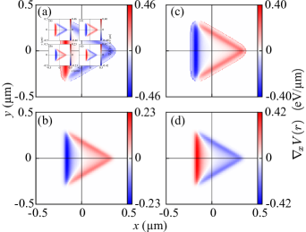
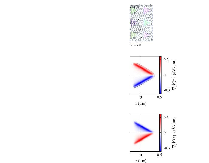
To investigate the effect of gate voltages on the asymmetry of the electrostatic potential, we performed the simulation by using FEniCS [60] which is based on the finite-element method. After extracting the electric displacement field near graphene, the spatially dependent capacitance of each gate was obtained, see Appendix D for details. Figure 7 shows exemplarily in-plane distributions of calculated for four different sequences of patterned gate and back gate voltages relevant to the experiments. The curves show that the asymmetry along the -direction is indeed present and can be reversed by reversing the polarity of one of the gates. In particular, in the discussed metamaterial the uniform bottom gate potential leads to a change of and thus of the lateral asymmetry parameter. This is because the applied back gate voltage is periodically screened by the graphite gate. It can even lead to the formation of lateral junctions. Note that the built-in potential was not included in the simulation.
Figures 3–6 show the following main qualitative features: i) a strong variation of the ratchet current amplitudes in the vicinity of the resistance maximum region; ii) a weak back and patterned gate dependence outside this gate voltage range; iii) the ratchet current may or may not change its sign upon switching the gate voltage polarity; iv) in most cases, the polarization-dependent and independent contributions have opposite signs for fixed gate sequences. Analogous arguments also apply to , whose gate voltage dependencies are presented in Appendix B. All these features can be qualitatively explained by the above theory. The sign of the ratchet current is defined by the product and/or , see Eqs. (8)–(10). Assuming that the spatial dependence of the near-field of diffraction does not reverse upon variation of the gate voltages, the sign of the ratchet current is solely defined by the sign of (negative for electrons and positive for holes) and . Therefore, if they both change sign, then the ratchet’s current direction remains unchanged. Otherwise, if one of the signs holds and the other reverses, the current direction is changed. As discussed above, the net current is a sum of the currents generated in two areas, above and outside the triangles. For this reason, for example, reversing the patterned gate voltages would change both, the sign of the electrostatic potential and the sign of () in the region outside the triangles, leaving the current direction unchanged, see e.g. in Fig. 6(b). Note that the part of the current that changes its sign with the patterned gate voltage variation, is responsible for the observed substantial change of the ratchet current amplitudes in the vicinity of the resistance maximum region, see Fig. 6(b). At the same time, the sign of is inverted above the triangles, while the carrier type remains unaffected, causing the sign inversion of the net current, see e.g. in Fig. 4(b).
V Summary
In summary, we demonstrate that the ratchet current can be efficiently generated in graphene-based 2D metamaterials excited by linearly polarized terahertz radiation. The directed current in response to an alternating electric field is caused by the asymmetry of the periodic electrostatic potential and the near-field diffraction formed by a patterned gate with an array of triangular antidots placed under a graphene layer and having a period much smaller than the radiation wavelength. Experimental data together with the developed theory demonstrate that the ratchet current consists of two contributions caused by the polarization-independent Seebeck ratchet effect and the DCDR mechanism. We show that in the studied structures with the patterned gate placed between graphene and the uniform back gate, the back gate voltage also introduces an asymmetry of the electrostatic potential. This is confirmed by the calculation using FEniCS [60] based on the finite-element method. The presence of two asymmetric potentials, which affect the lateral asymmetry parameter and lead to a periodic modification of the carrier density (carrier types) in the areas above and outside the triangular antidots, causes a complex dependence of the ratchet current on the gate voltages. Our analysis shows that while increasing the gate voltage increases the lateral asymmetry parameter, it does not lead to a corresponding increase of the ratchet current. This is due to the linear dispersion of graphene, for which increasing the gate potentials decreases the ratchet current.
VI Acknowledgments
The authors thank V.V. Bel’kov for valuable discussions. We acknowledge the financial support of the Deutsche Forschungsgemeinschaft (DFG, German Research Foundation) via Project-ID 314695032 – SFB 1277 (Subprojects A04 and A09), Project-ID 426094608, and of the Volkswagen Stiftung Program (97738). W.-H.K. and M.-H.L. gratefully acknowledge National Science and Technology Council of Taiwan (grant number: NSTC 112-2112-M-006-019-MY3). K.W. and T.T. acknowledge support from the Elemental Strategy Initiative conducted by the MEXT, Japan (Grant Number JPMXP0112101001) and JSPS KAKENHI (Grant Numbers 19H05790 and JP20H00354).
Appendix A Resistance map of sample A
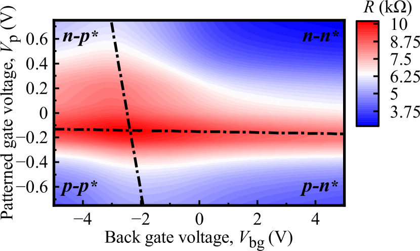
Figure A.1 shows the two-terminal sample resistance as a function of a patterned, , and back, , gate voltages. The data are obtained applying the standard lock-in technique with low modulation frequency ( Hz) and the source-drain current . The two-terminal resistance is controlled by both and , where mainly governs the carrier concentration in the graphene regions above the triangular holes, while influences the graphene regions around the holes. Therefore, by adjusting both gate voltages, the carrier density and modulation potential can be set indepedently [65]. Charge neutrality across the entire sample is achieved at , i.e., at the crossing point of the dash-dotted lines. This point deviates slightly from the expected zero voltages due to undesired background doping, which changes upon thermal cycling. Therefore, the gate positions in the resistance map in Fig. A.1 cannot be directly matched to the photovoltage data, as they were obtained in different cooldowns. When one gate voltage is fixed, sweeping the other gate yields resistance traces with a resistance maximum, similar to the charge neutrality point in unmodulated graphene. Those maxima occur along the two dash-dotted lines, which divide the map into four quadrants. Two of them correspond to the same carrier type inside and outside the triangular regions, the other two designate the bipolar regime, in which the carrier type inside and outside the triangular regions are opposite. We label those quadrants using and for electron and hole type, and mark the triangular regions with an asterisk (’*’). To determine the carrier densities, we carried out four-probe measurements of and for various gate voltages and at magnetic field . The Hall concentration was experimentally determined as , where is the Hall coefficient. In case of a fixed zero voltage on the back gate electrode, the 2D carrier density is also empirically given by cm-2, where and a gate offset are taken in volts.
Appendix B Gate dependencies of the photovoltage measured across Hall bar and additional results for the second sample
B.1 Gate dependencies of the photovoltage measured across Hall bar obtained for sample A
The polarization dependence of the photosignal measured across the contact pair 8-2 is well described by Eq. (5) being in full agreement with Eq. (14) of the theory developed for C1 symmetry. Figure B.1 shows the photosignal measured across the contact pair 8-2 as a function of the back gate voltage. The back gate dependencies of the individual contributions , and are obtained for zero patterned gate voltage. In line with the discussion presented in Sec. IV the contribution dominates the photoresponse for zero potentials at both gates, whereas sweeping the back gate voltage results in a complex variation of the signal magnitude and sign. Figure B.1 demonstrates that the amplitudes and twice reverse their sign while the sign of the amplitude remains unchanged in the whole range of the applied gate voltages.
Gate dependencies obtained varying one of the gate voltages and holding the other confirm a complexity of the gate dependencies. A double inversion of the signal sign is detected in the back gate dependencies for both positive and negative patterned gate voltages see Fig. B.2, whereas the signal change its sign only once if a high positive back gate voltage is applied and the patterned gate voltage is varied, see Fig. B.3(b). A single sign inversion of is also detected for high negative back gate voltage, see Fig. B.3(a). However, this dependence is characterized by a highly nonmonotonic behavior of all contributions in the vicinity of the resistance maximum.
As discussed above, these complex behavior is caused by the interplay of the lateral asymmetry parameter and the carrier density/type in the region above triangles, which is controlled by the back gate voltage.
B.2 Polarization and gate dependencies of the ratchet current obtained for sample B.
Figures B.4(a) and (b) show the polarization dependence of the photocurrent measured in sample B along the source-drain pair of contacts. The data are obtained for different values of the back gate voltage holding . The data are well described by Eq. (4) being in full agreement with Eq. (13) developed for C1 symmetry. To highlight the polarization dependence, in panels (a) and (b) we subtracted a small polarization-independent contribution. The overall behavior of the photocurrent is similar to that detected in sample A. Figure B.4(c) shows the back gate dependence of the individual contribution obtained by holding the patterned gate voltage at zero. The figure reveals that the contributions and dominate the signal in the whole range of the gate voltages. The former one reverses its sign in the vicinity of the resistance maximum and becomes almost constant at high back gate voltages. The polarization-independent contribution, by contrast, reverses sign three times.
Appendix C Extended description of the microscopic theory
The microscopic theory of the ratchet effect in graphene-based systems [4, 13] yields the following expressions for :
| (15a) | |||
| (15b) | |||
where is the Dirac fermion velocity in graphene and is the elementary charge. The contribution describes the so-called Seebeck ratchet effect caused by electron gas heating and simultaneous spatial charge redistribution and is given by [10]
| (16) |
where is the lattice temperature, and is the electron temperature relaxation time related with the electron-phonon interaction [10]. The polarization-dependent contributions to the ratchet current in Eqs. (15) are not related to the electron gas heating, but determined by the dynamic charge-density redistribution (DCDR) controlled solely by elastic scattering processes [66]. In particular, these terms are controlled by the dependence of the elastic scattering times on the electron energy, i.e. they are sensitive to the disorder potential. The values and were calculated in Refs. [4] and [13]:
| (17) | |||
| (18) | |||
| (19) |
Here is the Fermi energy, is the transport relaxation time which determines the electron mobility, is the relaxation time of the second angular harmonics of the electron distribution function, prime denotes differentiation over , and with . These expressions describe the frequency dependence of the DCDR-induced ratchet current which varies for different disorder potentials [4].
Appendix D Electrostatic simulations
The modeled device for the electrostatic simulation is considered under the geometry of the experimental device, but it contains part of triangle pattern, that is a triangle array, as shown in the rectangular box in Fig. D.1(a). In addition, we assume that the regions in the holes are vacuums because the hBN and SiO2 with the volume of such thin holes only slightly change the electric potential distribution. We set the dielectric constant of hBN and SiO2 to 3 and 3.9, respectively. Based on the periodicity of the triangle pattern, we focus on one period and set the origin at the equilateral triangle center in the following analysis.
FEniCS [60], a Python package for the finite-element method, combined with the mesh generator Gmsh [67], is adopted to numerically solve the Poisson equation in the modeled device and extract the electric displacement field near graphene. Figures D.1(b) and (c) are the spatially dependent capacitance of the Si back gate and the graphite patterned gate, respectively, calculated by dividing the induced carrier density by a unit gate voltage while the other gate is grounded. The induced carrier density can be calculated by the formula of surface charge density divided by the elementary charge
where is the unit normal vector of the surface of graphene and is the electric displacement field.
With the gate capacitors simulated and stored, the gate-dependent onsite potential is obtained by
| (20) |
where is the group velocity of the graphene, and the induced carrier density is obtained by summing over the contributions from all gates without the need of bothering with the electrostatic simulation again. Figures 7 and D.1(d), (e) show the partial-differentiated onsite potential or .
References
- Olbrich et al. [2009] P. Olbrich, E. L. Ivchenko, R. Ravash, T. Feil, S. D. Danilov, J. Allerdings, D. Weiss, D. Schuh, W. Wegscheider, and S. D. Ganichev, Ratchet effects induced by terahertz radiation in heterostructures with a lateral periodic potential, Phys. Rev. Lett. 103, 090603 (2009).
- Olbrich et al. [2011] P. Olbrich, J. Karch, E. L. Ivchenko, J. Kamann, B. März, M. Fehrenbacher, D. Weiss, and S. D. Ganichev, Classical ratchet effects in heterostructures with a lateral periodic potential, Phys. Rev. B 83, 165320 (2011).
- Kiselev and Golub [2011] Y. Y. Kiselev and L. E. Golub, Optical and photogalvanic properties of graphene superlattices formed by periodic strain, Phys. Rev. B 84, 235440 (2011).
- Nalitov et al. [2012] A. V. Nalitov, L. E. Golub, and E. L. Ivchenko, Ratchet effects in two-dimensional systems with a lateral periodic potential, Phys. Rev. B 86, 115301 (2012).
- Otsuji et al. [2013a] T. Otsuji, T. Watanabe, S. A. B. Tombet, A. Satou, W. M. Knap, V. V. Popov, M. Ryzhii, and V. Ryzhii, Emission and detection of terahertz radiation using two-dimensional electrons in III–v semiconductors and graphene, IEEE Trans. Terahertz Sci. Technol. 3, 63 (2013a).
- Drexler et al. [2013] C. Drexler, S. A. Tarasenko, P. Olbrich, J. Karch, M. Hirmer, F. Müller, M. Gmitra, J. Fabian, R. Yakimova, S. Lara-Avila, S. Kubatkin, M. Wang, R. Vajtai, P. M. Ajayan, J. Kono, and S. D. Ganichev, Magnetic quantum ratchet effect in graphene, Nat. Nanotechnol. 8, 104 (2013).
- Kurita et al. [2014] Y. Kurita, G. Ducournau, D. Coquillat, A. Satou, K. Kobayashi, S. B. Tombet, Y. M. Meziani, V. V. Popov, W. Knap, T. Suemitsu, and T. Otsuji, Ultrahigh sensitive sub-terahertz detection by InP-based asymmetric dual-grating-gate high-electron-mobility transistors and their broadband characteristics, Appl. Phys. Lett. 104, 251114 (2014).
- Budkin and Golub [2014] G. V. Budkin and L. E. Golub, Orbital magnetic ratchet effect, Phys. Rev. B 90, 125316 (2014).
- Faltermeier et al. [2015] P. Faltermeier, P. Olbrich, W. Probst, L. Schell, T. Watanabe, S. A. Boubanga-Tombet, T. Otsuji, and S. D. Ganichev, Helicity sensitive terahertz radiation detection by dual-grating-gate high electron mobility transistors, J. Appl. Phys. 118, 084301 (2015).
- Olbrich et al. [2016] P. Olbrich, J. Kamann, M. König, J. Munzert, L. Tutsch, J. Eroms, D. Weiss, M.-H. Liu, L. E. Golub, E. L. Ivchenko, V. V. Popov, D. V. Fateev, K. V. Mashinsky, F. Fromm, T. Seyller, and S. D. Ganichev, Terahertz ratchet effects in graphene with a lateral superlattice, Phys. Rev. B 93, 075422 (2016).
- Popov [2016] V. V. Popov, Polarization-dependent plasmonic photocurrents in two-dimensional electron systems, Appl. Phys. Lett. 108, 261104 (2016).
- Fateev et al. [2019] D. V. Fateev, K. V. Mashinsky, J. D. Sun, and V. V. Popov, Enhanced plasmonic rectification of terahertz radiation in spatially periodic graphene structures towards the charge neutrality point, Solid-State Electron. 157, 20 (2019).
- Hubmann et al. [2020] S. Hubmann, V. V. Bel’kov, L. E. Golub, V. Y. Kachorovskii, M. Drienovsky, J. Eroms, D. Weiss, and S. D. Ganichev, Giant ratchet magneto-photocurrent in graphene lateral superlattices, Phys. Rev. Research 2, 033186 (2020).
- Boubanga-Tombet et al. [2020] S. Boubanga-Tombet, W. Knap, D. Yadav, A. Satou, D. B. But, V. V. Popov, I. V. Gorbenko, V. Kachorovskii, and T. Otsuji, Room-temperature amplification of terahertz radiation by grating-gate graphene structures, Phys. Rev. X 10, 031004 (2020).
- Delgado-Notario et al. [2020] J. A. Delgado-Notario, V. Clericò, E. Diez, J. E. Velázquez-Pérez, T. Taniguchi, K. Watanabe, T. Otsuji, and Y. M. Meziani, Asymmetric dual-grating gates graphene FET for detection of terahertz radiations, APL Photonics 5, 066102 (2020).
- Mönch et al. [2022] E. Mönch, S. O. Potashin, K. Lindner, I. Yahniuk, L. E. Golub, V. Y. Kachorovskii, V. V. Bel’kov, R. Huber, K. Watanabe, T. Taniguchi, J. Eroms, D. Weiss, and S. D. Ganichev, Ratchet effect in spatially modulated bilayer graphene: Signature of hydrodynamic transport, Phys. Rev. B 105, 045404 (2022).
- Yahniuk et al. [2022] I. Yahniuk, G. V. Budkin, A. Kazakov, M. Otteneder, J. Ziegler, D. Weiss, N. N. Mikhailov, S. A. Dvoretskii, T. Wojciechowski, V. V. Bel’kov, W. Knap, and S. D. Ganichev, Terahertz ratchet effect in interdigitated hgte structures, Physical Review Applied 18, 054011 (2022).
- Tamura et al. [2022] K. Tamura, C. Tang, D. Ogiura, K. Suwa, H. Fukidome, Y. Takida, H. Minamide, T. Suemitsu, T. Otsuji, and A. Satou, Fast and sensitive terahertz detection with a current-driven epitaxial-graphene asymmetric dual-grating-gate field-effect transistor structure, APL Photonics 7, 126101 (2022).
- Mönch et al. [2023] E. Mönch, S. O. Potashin, K. Lindner, I. Yahniuk, L. E. Golub, V. Y. Kachorovskii, V. V. Bel’kov, R. Huber, K. Watanabe, T. Taniguchi, J. Eroms, D. Weiss, and S. D. Ganichev, Cyclotron and magnetoplasmon resonances in bilayer graphene ratchets, Phys. Rev. B 107, 115408 (2023).
- Mönch et al. [2023] E. Mönch, S. Hubmann, I. Yahniuk, S. Schweiss, V. V. Bel’kov, L. E. Golub, R. Huber, J. Eroms, K. Watanabe, T. Taniguchi, D. Weiss, and S. D. Ganichev, Nonlinear intensity dependence of ratchet currents induced by terahertz laser radiation in bilayer graphene with asymmetric periodic grating gates, J. Appl. Phys. 134, 10.1063/5.0165248 (2023).
- Jülicher et al. [1997] F. Jülicher, A. Ajdari, and J. Prost, Modeling molecular motors, Rev. Mod. Phys. 69, 1269 (1997).
- Linke [2002] H. Linke, Ratches and brownian motors: Basics, experiments and applications, Appl. Phys. A 75, 167 (2002).
- Reimann [2002] P. Reimann, Brownian motors: Noisy transport far from equilibrium, Phys. Rep. 361, 57 (2002).
- Hänggi and Marchesoni [2009] P. Hänggi and F. Marchesoni, Artificial brownian motors: Controlling transport on the nanoscale, Rev. Mod. Phys. 81, 387 (2009).
- Denisov et al. [2014] S. Denisov, S. Flach, and P. Hänggi, Tunable transport with broken space–time symmetries, Phys. Rep. 538, 77 (2014).
- Ivchenko and Ganichev [2011] E. L. Ivchenko and S. D. Ganichev, Ratchet effects in quantum wells with a lateral superlattice, JETP Lett. 93, 673 (2011), [Pisma v ZhETF 93, 752 (2011)].
- Bercioux and Lucignano [2015] D. Bercioux and P. Lucignano, Quantum transport in rashba spin–orbit materials: a review, Reports on Progress in Physics 78, 106001 (2015).
- Budkin et al. [2016] G. V. Budkin, L. E. Golub, E. L. Ivchenko, and S. D. Ganichev, Magnetic ratchet effects in a two-dimensional electron gas, JETP Lett. 104, 649 (2016).
- David Cubero [2016] F. R. David Cubero, Brownian Ratchets: From Statistical Physics to Bio and Nano-motors (2016) p. 13–26.
- Reichhardt and Reichhardt [2017] C. J. O. Reichhardt and C. Reichhardt, Ratchet effects in active matter systems, Annu. Rev. Condens. Matter Phys. 8, 51 (2017).
- Lau and Kedem [2020] B. Lau and O. Kedem, Electron ratchets: State of the field and future challenges, The Journal of Chemical Physics 152, 200901 (2020), https://doi.org/10.1063/5.0009561 .
- Ermann and Shepelyansky [2011] L. Ermann and D. L. Shepelyansky, Relativistic graphene ratchet on semidisk galton board, Eur. Phys. J. B 79, 357 (2011).
- Bisotto et al. [2011] I. Bisotto, E. S. Kannan, S. Sassine, R. Murali, T. J. Beck, L. Jalabert, and J.-C. Portal, Microwave based nanogenerator using the ratchet effect in si/sige heterostructures, Nanotechnology 22, 245401 (2011).
- Kannan et al. [2012] E. S. Kannan, I. Bisotto, J.-C. Portal, T. J. Beck, and L. Jalabert, Energy free microwave based signal communication using ratchet effect, Appl. Phys. Lett. 101, 143504 (2012).
- Coquillat et al. [2010] D. Coquillat, S. Nadar, F. Teppe, N. Dyakonova, S. Boubanga-Tombet, W. Knap, T. Nishimura, T. Otsuji, Y. M. Meziani, G. M. Tsymbalov, and V. V. Popov, Room temperature detection of sub-terahertz radiation in double-grating-gate transistors, Optics Express 18, 6024 (2010).
- Knap et al. [2010] W. Knap, S. Nadar, H. Videlier, S. Boubanga-Tombet, D. Coquillat, N. Dyakonova, F. Teppe, K. Karpierz, J. Łusakowski, M. Sakowicz, I. Kasalynas, D. Seliuta, G. Valusis, T. Otsuji, Y. Meziani, A. E. Fatimy, S. Vandenbrouk, K. Madjour, D. Théron, and C. Gaquière, Field effect transistors for terahertz detection and emission, J. Infrared Millim. Terahertz Waves 32, 618 (2010).
- Popov et al. [2011] V. V. Popov, D. V. Fateev, T. Otsuji, Y. M. Meziani, D. Coquillat, and W. Knap, Plasmonic terahertz detection by a double-grating-gate field-effect transistor structure with an asymmetric unit cell, Appl. Phys. Lett. 99, 243504 (2011).
- Watanabe et al. [2013a] T. Watanabe, Y. Kurita, A. Satou, T. Suemitsu, W. Knap, V. V. Popov, and T. Otsuji, Terahertz monochromatic coherent emission from an asymmetric chirped dual-grating-gate InP-HEMT with a photonic vertical cavity, in 2013 38th International Conference on Infrared, Millimeter, and Terahertz Waves (IRMMW-THz) (IEEE, 2013).
- Popov [2013] V. V. Popov, Terahertz rectification by periodic two-dimensional electron plasma, Appl. Phys. Lett. 102, 253504 (2013).
- Watanabe et al. [2013b] T. Watanabe, S. A. Boubanga-Tombet, Y. Tanimoto, D. Fateev, V. Popov, D. Coquillat, W. Knap, Y. M. Meziani, Y. Wang, H. Minamide, H. Ito, and T. Otsuji, InP- and GaAs-based plasmonic high-electron-mobility transistors for room-temperature ultrahigh-sensitive terahertz sensing and imaging, IEEE Sensors Journal 13, 89 (2013b).
- Otsuji et al. [2013b] T. Otsuji, T. Watanabe, S. A. B. Tombet, A. Satou, V. Ryzhii, V. Popov, and W. Knap, Emission and detection of terahertz radiation using two-dimensional plasmons in semiconductor nanoheterostructures for nondestructive evaluations, Optical Engineering 53, 031206 (2013b).
- Boubanga-Tombet et al. [2014] S. Boubanga-Tombet, Y. Tanimoto, A. Satou, T. Suemitsu, Y. Wang, H. Minamide, H. Ito, D. V. Fateev, V. V. Popov, and T. Otsuji, Current-driven detection of terahertz radiation using a dual-grating-gate plasmonic detector, Appl. Phys. Lett. 104, 262104 (2014).
- Popov et al. [2015] V. V. Popov, D. V. Fateev, E. L. Ivchenko, and S. D. Ganichev, Noncentrosymmetric plasmon modes and giant terahertz photocurrent in a two-dimensional plasmonic crystal, Phys. Rev. B 91, 235436 (2015).
- Rozhansky et al. [2015] I. Rozhansky, V. Kachorovskii, and M. Shur, Helicity-driven ratchet effect enhanced by plasmons, Phys. Rev. Lett. 114, 246601 (2015).
- Spisser et al. [2015] H. Spisser, A.-S. Grimault-Jacquin, N. Zerounian, A. Aassime, L. Cao, F. Boone, H. Maher, Y. Cordier, and F. Aniel, Room-temperature AlGaN/GaN terahertz plasmonic detectors with a zero-bias grating, J. Infrared Millim. Terahertz Waves 37, 243 (2015).
- Koseki et al. [2016] Y. Koseki, V. Ryzhii, T. Otsuji, V. V. Popov, and A. Satou, Giant plasmon instability in a dual-grating-gate graphene field-effect transistor, Phys. Rev. B 93, 245408 (2016).
- Fateev et al. [2017] D. V. Fateev, K. V. Mashinsky, H. Qin, J. Sun, and V. V. Popov, Giant effect of terahertz-radiation rectification in periodic graphene plasmonic structures, Semiconductors+ 51, 1500 (2017).
- Rupper et al. [2018] G. Rupper, S. Rudin, and M. S. Shur, Ratchet effect in partially gated multifinger field-effect transistors, Phys. Rev. Applied 9, 064007 (2018).
- Yu [2018] A. Yu, Plasmon ratchet effect with electrons and holes simultaneously existing in the graphene channel: A promising effect for the terahertz detection, J. Phys. D: Appl. Phys. 51, 395103 (2018).
- Sai et al. [2021] P. Sai, S. O. Potashin, M. Szoła, D. Yavorskiy, G. Cywiński, P. Prystawko, J. Łusakowski, S. D. Ganichev, S. Rumyantsev, W. Knap, and V. Y. Kachorovskii, Beatings of ratchet current magneto-oscillations in GaN-based grating gate structures: Manifestation of spin-orbit band splitting, Phys. Rev. B 104, 045301 (2021).
- Otsuji et al. [2022] T. Otsuji, S. A. Boubanga-Tombet, A. Satou, D. Yadav, H. Fukidome, T. Watanabe, T. Suemitsu, A. A. Dubinov, V. V. Popov, W. Knap, V. Kachorovskii, K. Narahara, M. Ryzhii, V. Mitin, M. S. Shur, and V. Ryzhii, Graphene-based plasmonic metamaterial for terahertz laser transistors, Nanophotonics 11, 1677 (2022).
- Delgado-Notario et al. [2022] J. A. Delgado-Notario, W. Knap, V. Clericò, J. Salvador-Sánchez, J. Calvo-Gallego, T. Taniguchi, K. Watanabe, T. Otsuji, V. V. Popov, D. V. Fateev, E. Diez, J. E. Velázquez-Pérez, and Y. M. Meziani, Enhanced terahertz detection of multigate graphene nanostructures, Nanophotonics 11, 519 (2022).
- Xu et al. [2009] X. Xu, N. M. Gabor, J. S. Alden, A. M. van der Zande, and P. L. McEuen, Photo-thermoelectric effect at a graphene interface junction, Nano Lett. 10, 562 (2009).
- Mueller et al. [2010] T. Mueller, F. Xia, and P. Avouris, Graphene photodetectors for high-speed optical communications, Nat. Photonics 4, 297 (2010).
- Yan et al. [2012] J. Yan, M.-H. Kim, J. A. Elle, A. B. Sushkov, G. S. Jenkins, H. M. Milchberg, M. S. Fuhrer, and H. D. Drew, Dual-gated bilayer graphene hot-electron bolometer, Nat. Nanotechnol. 7, 472 (2012).
- Echtermeyer et al. [2014] T. J. Echtermeyer, P. S. Nene, M. Trushin, R. V. Gorbachev, A. L. Eiden, S. Milana, Z. Sun, J. Schliemann, E. Lidorikis, K. S. Novoselov, and A. C. Ferrari, Photothermoelectric and photoelectric contributions to light detection in metal–graphene–metal photodetectors, Nano Lett. 14, 3733 (2014).
- Cai et al. [2014] X. Cai, A. B. Sushkov, R. J. Suess, M. M. Jadidi, G. S. Jenkins, L. O. Nyakiti, R. L. Myers-Ward, S. Li, J. Yan, D. K. Gaskill, T. E. Murphy, H. D. Drew, and M. S. Fuhrer, Sensitive room-temperature terahertz detection via the photothermoelectric effect in graphene, Nat. Nanotechnol. 9, 814 (2014).
- Sassine et al. [2008] S. Sassine, Y. Krupko, J.-C. Portal, Z. D. Kvon, R. Murali, K. P. Martin, G. Hill, and A. D. Wieck, Experimental investigation of the ratchet effect in a two-dimensional electron system with broken spatial inversion symmetry, Phys. Rev. B 78, 045431 (2008).
- Kannan et al. [2011] E. S. Kannan, I. Bisotto, J.-C. Portal, R. Murali, and T. J. Beck, Photovoltage induced by ratchet effect in si/sige heterostructures under microwave irradiation, Applied Physics Letters 98, 193505 (2011), https://doi.org/10.1063/1.3590255 .
- Logg et al. [2012] A. Logg, K.-A. Mardal, and G. Wells, eds., Automated Solution of Differential Equations by the Finite Element Method: The FEniCS Book (Springer Berlin Heidelberg, 2012).
- Ganichev [1999] S. D. Ganichev, Tunnel ionization of deep impurities in semiconductors induced by terahertz electric fields, Phys. B 273-274, 737 (1999).
- Glazov and Ganichev [2014] M. M. Glazov and S. D. Ganichev, High frequency electric field induced nonlinear effects in graphene, Phys. Rep. 535, 101 (2014).
- Candussio et al. [2020] S. Candussio, M. V. Durnev, S. A. Tarasenko, J. Yin, J. Keil, Y. Yang, S.-K. Son, A. Mishchenko, H. Plank, V. V. Bel’kov, S. Slizovskiy, V. Fal’ko, and S. D. Ganichev, Edge photocurrent driven by terahertz electric field in bilayer graphene, Phys. Rev. B 102, 045406 (2020).
- Note [1] Note that, in the structure under study, the size of the triangles is much larger than the carrier mean free path. Therefore, the mechanism suggested in Ref. [68] and used for description of experimental data in Refs. [58, 59] is not applicable to our system.
- Drienovsky et al. [2018] M. Drienovsky, J. Joachimsmeyer, A. Sandner, M.-H. Liu, T. Taniguchi, K. Watanabe, K. Richter, D. Weiss, and J. Eroms, Commensurability oscillations in one-dimensional graphene superlattices, Phys. Rev. Lett. 121, 026806 (2018).
- Faltermeier et al. [2018] P. Faltermeier, G. V. Budkin, S. Hubmann, V. V. Bel’kov, L. E. Golub, E. L. Ivchenko, Z. Adamus, G. Karczewski, T. Wojtowicz, D. A. Kozlov, D. Weiss, and S. D. Ganichev, Circular and linear magnetic quantum ratchet effects in dual-grating-gate CdTe-based nanostructures, Phys. E 101, 178 (2018).
- Geuzaine and Remacle [2009] C. Geuzaine and J. Remacle, Gmsh: A 3-d finite element mesh generator with built-in pre- and post-processing facilities, International Journal for Numerical Methods in Engineering 79, 1309 (2009).
- Chepelianskii et al. [2008] A. D. Chepelianskii, M. V. Entin, L. I. Magarill, and D. L. Shepelyansky, Ratchet transport of interacting particles, Phys. Rev. E 78, 041127 (2008).