Terahertz plasmonic resonances in coplanar graphene nanoribbon structures
Abstract
We analyze plasmonic oscillations in the coplanar graphene nanoribbon (GNR) structures induced by the applied terahertz (THz) signals and calculate the GNR impedance. The plasmonic oscillations in the CNR structures are associated with the electron and hole inductances and the lateral inter-CNR capacitance. A relatively low inter-GNR capacitance enables the resonant excitation of the THz plasmonic oscillations in the CNR structures with long GNRs. The GNR structures under consideration can be used in different THz devices as the resonant structures incorporated in THz detectors, THz sources using resonant-tunneling diodes, photomixers, and surface acoustic wave sensors.
I Introduction
Due to the remarkable properties of graphene layers (GLs) (high intrinsic mobility enabling an elevated electrical conductivity, high thermal conductivity, transparency to light, and mechanical strength), GLs are very attractive for different device applications. In particular, graphene micro- and nanoribbons can be used in the detectors and sources of electromagnetic radiation, surface acoustic wave sensors, power and flexible devices [1, 2, 3, 4, 5, 6, 7, 8, 9, 10, 11, 12, 13, 14]. The possibility of the terahertz (THz) plasmonic wave excitation in the graphene structures [2, 3, 4, 7, 8, 9, 10, 15, 16, 17, 18, 19, 20, 21, 22, 23] markedly enhances the functionality of the graphene-based devices. The structures with GLs partitioned into arrays of graphene nanoribbons (GNRs) have also been already studied (for example, [24, 25, 26, 27, 28, 29]). In this work, we focused mainly on the plasmonic waves propagating perpendicular to the GNRs aiming the achievement of the plasmonic resonances at relatively high frequencies, particularly, in the frequencies corresponding to the mid-infrared range.
In the present paper, we explore the structures comprising two co-planar GNRs on a dielectric substrate focusing on their terahertz applications. In such structures the plasmonic wave number is determined by the GNR length, which is much longer than their widths. As a result, the perpendicular plasmonic modes are not excited in the frequency range under consideration (the THz range).
It is assumed that the bias dc voltage and the THz signal voltage with the frequency are applied between the GNR edges. The bias voltage results in the formation of the two-dimensional electron and hole systems, 2DES and 2DHS. The signal voltage can be produced by the impinging electromagnetic radiation and received by an antenna integrated with the GNR structure. The THz signals excite the plasmonic standing waves (plasmonic oscillations) in the GNRs. Examining the plasmonic properties of the co-planar GNRs, we show that with a relatively low geometrical inter-GNR capacitance, the plasmonic resonances can be in the THz range even for fairly long GNRs. This property of the coplanar GNRs, as well as their lateral periodic arrays, can find applications in different devices using the THz plasmonic resonant structures.
II Equations of the model
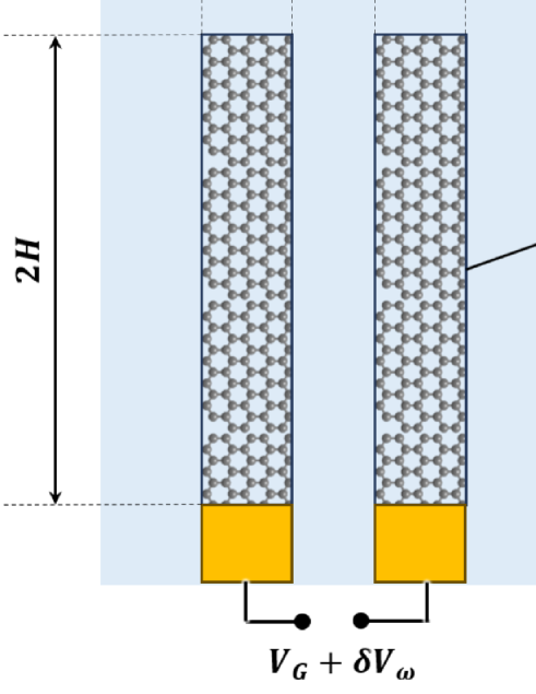


Considering the co-planar GNR structures, we assume two types of signal voltage bias, P-GNR and S-GNR, as shown in Fig. 1(a) and Fig. 1(b). The lengths and widths of the GNRs are and , respectively, whereas the spacing between the GNRs is equal to being much smaller than other geometrical parameters ( ).
The GNR potentials are , where the signs ”+” and ”-” correspond to the GNRs to which the voltages of different polarities are applied. The displacement current density between the GNRs and the continuity equations for the electrons and holes governing their transport along the GNRs can be presented as
| (1) |
| (2) |
Here
| (3) |
and
| (4) |
are the GNR ac conductivity and the geometrical inter-GNR geometrical capacitance, respectively, where is the dc Drude conductivity of a GNR with the carrier Fermi energy and the carrier collision frequency (scattering by impurities and acoustic phonons), and are the effective dielectric constant and the substrate dielectric constant (the dielectric constant of the media above the structure is assumed to be unity), the factor
reflects the GNR blade-like shape [30] (see also Refs. [31, 32, 33, 34, 35]) with parameter .
The electron and hole Fermi energy in the pertinent GNR is determined by the bias voltage : , where cm/s is the characteristic electron and hole velocity in graphene, the steady-state electron and hole density, and is the Planck constant.
Using Eqs. (1) - (3), we arrive at the following equations governing the potentials :
| (5) |
| (6) |
with being the characteristic velocity of the plasmonic wave along the GNRs. Depending on the signal voltage application, the boundary conditions for Eqs. (5) and (6) are:
| (7) |
for the situation corresponding to the device corresponding to structure Fig 1(a) P-GNR, and
| (8) |
for the device shown in Fig. 1(b) - interdigital GNR connection S-GNR.
III Plasmonic oscillations
Equations (5) and (6) with the boundary conditions given by Eqs.(7) and (8) for the local signal voltage swing between the GNRs result in
| (9) |
and
| (10) |
for the P- and S GNR structures, respectively.
Here
| (11) |
where
| (12) |
is the characteristic frequency of the plasmonic oscillation fundamental mode in the GNRs. Considering the dependence of on , we obtain
| (13) |
In particular, for (), meV, m, m (), m, Eq. (15) yields THz.
Equations (9) and (10) describe the spatial distributions of the self-consistent potential and carrier densities in the GNRs (along them), i.e., the plasmonic oscillations (the standing plasmonic waves with the frequency and the normalized wave number . AS follows from Eqs. (9) and (10), the relative amplitudes of the ac potential and can be markedly larger than unity when the denominators in right-hand sides of these equations and at certain signal frequencies (the plasmonic resonant frequencies).
Deriving Eqs. (5),(6), (9), and (10), we disregarded the ac potential nonuniformity across the GNRs (in the -direction), i.e., neglected the plasmonic oscillation longitudinal modes with the wave vectors directed perpendicular to the GNR. Such modes correspond to higher harmonics. This restricts our consideration by the condition (assumed above).
Figure 2 shows the dependences of the plasmonic frequency on the bias voltage for different GNR geometries calculated using Eq. (13) with Eq. (4). It is assumed that , m, and . In line with Eq. (12), an increase in the bias voltage leads to an increase in the characteristic plasmonic frequency due to the carrier density and the carrier Fermi energy rise when increases. The plasmonic frequency is sensitive to the geometrical parameters and , which determine the carrier density and the GNR ac conductivity. The specifics of the GNR structures under consideration lead to relatively small inter-GNR capacitance and elevated values of the plasmonic wave velocity . Consequently, rather high values of plasmonic frequency (in the THz range) can be realized at fairly large lengths of the GNRs.
IV GNR structure admittance and impedance
The net inter-GNR displacement current is given by
| (14) |
with the current density given by Eq. (9) or Eq. (10). For the admittance of GNR structure under consideration , we obtain (for the P- and S-devices, respectively)
| (15) |
The impedances of the P-GNRs and S-GNRs are given by
| (16) |
At low signal frequencies () the admittances and impedances of both GNR structures tend to zero and infinity, respectively, provided the inter-GNR leakage current is insignificant. In the range of elevated frequencies comparable with the characteristic plasmonic frequency , the admittances and impedances exhibit the oscillations associated with the plasmonic response of the carriers in the GNRs.
Figures 3 and 4 show the P-GNRs and S-GNRs spectral characteristics.
As follows from the analysis of the frequency characteristics of the P-GNRs described by the first Eq. (15), Re exhibits maxima at , where is the plasmonic resonance index, i.e., when . At these frequencies, the peak height is proportional to the plasmonic oscillations quality factor being weakly dependent on the resonance index. The first maxima of the curves in Fig. 3(a) correspond to and 1.09 THz (dashed and solid lines). The second maximum for THz corresponds to THz. Comparison of Figs. 3(a) and 3(b) shows that the maxima of Re at correspond to a sharp change in the sign of Im (so that Im ). In contrast, Re versus dependences, given by the first Eq. (16), exhibit maxima at [see Fig.3(c)], i.e., at () with the peak height proportional to . Simultaneously, Im turns to zero when . This is in line with the plots in Fig. 3(d).
The frequency dependences of the S-GNR admittance shown in Fig. 4 differ from those for the P-GNRs. This is due to different conditions of the plasmonic resonances. Indeed, considering the second Eq. (15), one can see that the maxima of Re correspond to resonant frequencies , which satisfy the condition . This condition yields: (”soft” mode) and with . As seen from Figs. 4(a) and 4(b), the positions of the maximum of Re and the point, where Im are close to (for THz) and to THz (for THz). As can be derived using the second Eq. (15), the height of the Re maxima is proportional to , demonstrating a substantial decrease with increasing plasmonic index and the fact that the peak height is generally lower than the pertinent peaks of the P-GNR admittance. Such a dependence of Re on is clearly seen in Fig. 4(a). In particular, the ratio .
It is interesting that in both P- and S-GNRs the Re and exhibit maxima at approximately the same frequencies having approximately the same height (compare Figs. 3(c) and (4c).
One notes that the resonant frequencies at which Im , Im , Im , and Im equal to zero correspond to very low values of Re and Re .
The sharpness of the resonant peaks substantially depends on the carrier collision frequency . An increase in the ratio (i.e., the inverse plasmonic oscillations quality factor ) leads to the pertinent lowering of the resonant peak heights. This implies that the realization of the GNR structures exhibiting pronounced plasmonic resonances requires using sufficiently perfect GNRs or lowering the operation temperature down from room temperature.
V Discussion and comments
The structures based on the vertically stacked separately contacted GLs and GNRs with the hBN, WS2, Al2O3, and other insulating layers were studied and used in different devices (optical and infrared modulators and detectors, THz detectors, THz detectors and photomixers, and others[36, 37, 38, 39, 40, 41, 42, 43, 44, 45]. The resonant plasmonic effects in such structures can lead to a substantial enhancement of device characteristics. The resonant plasmonic response in the lateral co-planar structures with separately contacted GNRs, considered above, is akin to that in the vertically stacked multiple-GL structures [40]. However, as predicted above, the lateral coplanar GNR structures can exhibit a pronounced plasmonic response controlled by the bias voltage even when the GNRs are relatively long (about several micrometers). This is because the plasmonic frequency in such structures is determined by the inter-GNR geometrical capacitance. This capacitance can be much smaller than the capacitance of the vertically stacked GLs. Indeed, the geometrical capacitance (per unit of the GNR length) of the lateral structure with two coplanar GNRs considered above is given by , whereas the geometrical capacitance of the vertically stacked GNRs of the same lateral sizes separated by the spacing is equal , hence
| (17) |
Comparing the plasmonic frequencies of co-planar and vertically stacked GNRs, and , and assuming that GNR lengths are equal to and , respectively, we obtain
| (18) |
if the carrier Fermi energy (carrier density) in the GNR structures is the same, and
| (19) |
for equal bias voltages, , applied between the GNRs. Considering that in the devices with the vertically stacked GNRs the thickness of the inter-GNR dielectric layer is relatively small and setting m, m (), m, and , we find . This implies that in the coplanar GNR structures the same plasmonic frequency can be realized at much longer GNRs ().
As has been shown previously, the plasmonic resonances in the structures with the arrays of several vertically stacked GNRs (GNR stacks) can be more pronounced [17, 18, 27]. The results obtained above can be applied for the lateral arrays vertically stacked GNRs the proper renormalization of the characteristic plasmonic frequency given by Eq. (12). In the case when the GNR stack comprises non-Bernal stacked GNRs, the electron and hole density in each GNR is equal to . Hence, for the carrier Fermi energy , which determines the GNR Drude conductivity, we obtain . Accounting for that the net GNR stack conductivity is proportional to , for the renormalized plasmonic frequency we find .
In principle, the plasmonic waves along the lateral depleted channel formed in the graphene p-n- junction predicted previously [46] resemble those considered above. However, there is a substantial difference between the plasmonic waves associated with the oscillating charges localized in the isolated GNRs, considered by us, and the plasmonic waves associated with the residual charges in the depleted area in graphene lateral p-n junctions.
The voltage-controlled coplanar GNR plasmonic resonators can be used in the THz detectors exploiting the signal rectification in p-i-n diodes and the THz radiation sources based on the resonant-tunneling diodes. In the first case, an enhanced real part of the GNR structures admittance at the plasmonic resonances promotes the rectified current amplification, which leads to an elevated detector responsivity. In the second case, low values of the real part of the GNR resonant impedance, can support the THz oscillation self-excitation and radiation emission.
Using periodic coplanar S-GNR structures with multiple GNR pairs can simplify the problem matching of these structures with the external circuits (i.r., with a load resistance or a THz antenna). These structures might bealso used for the THz photomixers exploiting the plasmonic resonances, GNR optical transparency, and strong light absorption in underlying layers, as well as for the acoustic and photoacoustic transducers.
Conclusions
We explored the plasmonic response of the lateral coplanar GNR structures to the impinging radiation. The pertinent resonant frequencies are determined by the plasmonic frequencies, which can fall into the THz range in structures with fairly long GNRs (about several micrometers). Due to the sensitivity of the plasmonic frequency to the bias voltage, the resonant response can be effectively voltage-controlled. The coplanar GNR structures and their version with multiple interdigital GNRs can serve as the resonant cavities for different passive and active THz devices, including THz detectors, photomixers using the interband transitions in the structure substrate (photoconductive antenna), oscillators with the diodes exhibiting negative dynamic conductivity (for example, resonant-tunneling diodes), and the acoustic transducers.
Acknowledgments
The work at RIEC, FRIIS, and UoA was supported by the Japan Society for Promotion of Science (KAKENHI Nos. 21H04546, 20K20349), Japan. The work at RPI was supported by AFOSR (contract number FA9550-19-1-0355).
Data availability
All data that support the findings of this study are available within the article.
References
- [1] P. Avouris, Z. Chen, and V. Perebeinos, “Carbon-based electronics,” Nat. Nanotech. 2, 605 (2007).
- [2] V. Ryzhii, T. Otsuji, and M. Shur, “Graphene based plasma-wave devices for terahertz applications,” Appl. Phys. Lett., 116, 140501 (2020).
- [3] M. Shur, G. Aizin, T. Otsuji, and V. Ryzhii “Plasmonic field-effect transistors (TeraFETs) for 6G communications,” Sensors, 21, 7907 (2021).
- [4] T. Otsuji, S.A. Boubanga-Tombet, A. Satou, D. Yadav, H. Fukidome, T. Watanabe, T. Suemitsu, A.A. Dubinov, V.V. Popov, W. Knap, V. Kachorovskii, K. Narahara, M. Ryzhii, V. Mitin, M.S. Shur, and V. Ryzhii, “Graphene-based plasmonic metamaterial for terahertz laser transistors,” Nanophoton. 11,1677 (2022).
- [5] V. Ryzhii,M. Ryzhii, A. Satou, T. Otsuji, M. Ryzhii, V. Mitin, M. S. Shur, and T. Otsuji, “Ballistic injection terahertz plasma instability in graphene n+-i-n-n+ field-effect transistors and lateral diodes, ” Phys. Stat. Solidi A 219,2100694 (2022).
- [6] L. Wang, N. An, S. Gong, X. Sheng, Y. Li, B. Yao, C. Yu, Z. He, Q. Liu, Z. Feng, T. Otsuji, and Y. Zhang “Ultrafast terahertz transparency boosting in graphene meta-cavities,” Nanophoton., 11, 4899 (2022).
- [7] M. Ryzhii, V. Ryzhii, M. S. Shur, V. Mitin, C. Tang, and T. Otsuji, “Terahertz bolometric detectors based on graphene field-effect transistors with the composite h-BN/black-P/h-BN gate layers using plasmonic resonances,” J. Appl. Phys., vol. 134, no. 8, 084501, 2023.
- [8] V. Ryzhii, C. Tang, T. Otsuji, M. Ryzhii, V. Mitin, and M. S. Shur “Effect of electron thermal conductivity on resonant plasmonic detection in terahertz hot-electron bolometers based on metal/black-AsP/graphene FETs,” Phys. Rev. Appl. 19, 064033( 2023).
- [9] V. Ryzhii, C. Tang, T. Otsuji, M. Ryzhii, V. Mitin, and M.S. Shur “Hot-electron resonant terahertz bolometric detection in the graphene/black-AsP field-effect transistors with a floating gate,” J. Appl. Phys. 133, 174501 (2023).
- [10] K. Tamura, C. Tang, D. Ogiura, K. Suwa, H. Fukidome, Y. Takida, H. Minamide, T. Suemitsu, T. Otsuji, and A. Satou, “Fast and sensitive terahertz detection in a current-driven epitaxial-graphene asymmetric dual-grating-gate FET structure,” APL Photonics 7, 16101 (2022).
- [11] X. Guo, J. An, H. Wu, Z. Cai, and P. Wang, “Graphene acoustic transducers based on electromagnetic interactions,” Ultrasonics 114, 106420 (2021).
- [12] J. He, Z. Fang, C. Gao, W. Zhang, X. Guan, and J. Lin, “Graphene enhanced flexible piezoelectric transducers for dynamic strain measurement: from material preparation to application,” Smart Mater. Struct. 32, 025012 (2023).
- [13] X. Guo, Y. Zhang, J. An, Q. Zhang, R. Wang, and X. Yu, “Experimental investigation on characteristics of graphene acoustic transducers driven by electrostatic and electromagnetic forces,” Ultrasonics 127, 1064857 (2023)
- [14] M. Šiškins, M. Lee, D. Wehenkel, R. van Rijn, T. W. de Jong, J. R. Renshof, B. C. Hopman, W. S. J. M. Peters, D. Davidovikj, H. S. J. van der Zant, and P. G. Steeneken, “Sensitive capacitive pressure sensors based on graphene membrane arrays,” Microsyst. Nanoeng. 6, 102 (2020).
- [15] V. Ryzhii, A. Satou, and T. Otsuji, “Plasma waves in two-dimensional electron-hole system in gated graphene heterostructures,” J. Appl. Phys. 101, 024509 (2007).
- [16] H. Yan, X. Li, B. Chandra, G. Tulevski, Y. Wu, M. Freitag, W. Zhu, P. Avouris, and F. Xia, “Tunable infrared plasmonic devices using graphene/insulator stacks,” Nat. Nanotech. 7, 330 (2012).
- [17] N. K. Emani, D. Wang, T.-F. Chung, L. J. Prokopeva, A. V. Kildishev, V. M. Shalaev, Y. P. Chen, and A. Boltasseva, “Plasmon resonance in multilayer graphene nanoribbons,” Laser Photonics Reviews 9, 650 (2015). nm.
- [18] D. Svintsov, Zh. Devizorova, T. Otsuji, and V. Ryzhii, “Plasmons in tunnel-coupled graphene layers: backward waves with quantum cascade gain,” Phys. Rev. B. 94, 115301 (2016).
- [19] D. Rodrigo, A. Tittl, O. Limaj, F. J. G. de Abajo, V. Pruneri, and H. Altug, “Double-layer graphene for enhanced tunable infrared plasmonics,” Light: Science Applications 6, e16277 (2017).
- [20] G. Li, V. Semenenko, V. Perebeinos, and P. Liu, “Multilayer graphene terahertz plasmonic structures for enhanced frequency tuning range,” ACS Photonics 6, 3180 (2019).
- [21] S. Ogawa, S. Fukushima, and M. Shimatani, “Graphene plasmonics in sensor applications: A Review,” Sensors (Basel) 20, 3563 (2020).
- [22] L. Wang, N. An, Xu-s. He, X. Zhang A. Zhu, B. Yao,and Y. Zhang, “Dynamic and active THz graphene metamaterial devices,” Nanomaterials (Basel) 17, 2097 (2022)
- [23] S. Gong, L. Wang, Y. Zhang, Z. Yang, X. Li, Q. Wen, Z. He, S. Liang, L. Yuan, C. Yu, Z. Feng, Z. Yang, and X. Zhang, “Ultra-extraordinary optical transmission induced by cascade coupling of surface plasmon polaritons in composite graphene–dielectric stack,” Opt.Express 28, 30502 (2020)
- [24] V. V. Popov, O. V. Polischuk, A. R. Davoyan, V. Ryzhii, T. Otsuji, and M. S. Shur, “Plasmonic terahertz lasing in an array of graphene nanocavities,” Phys. Rev. B 86, 1955437 (2012).
- [25] P. A. D. Goncalves, E. J. C. Dias, Y. V. Bludov, and N. M. R. Peres, “Modeling the excitation of graphene plasmons in periodic grids of graphene ribbons: An analytical approach,” Phys. Rev. B 94, 195421 (2016).
- [26] L. Xiong, C. Forsythe, M. Jung, A. S. McLeod, S. S. Sunku, Y. M. Shao, G. X. Ni, A. J. Sternbach, S. Liu, J. H. Edgar, E. J. Mele, M. M. Fogler, G. Shvets, C. R. Dean, and D. N. Basov, “Photonic crystal for graphene plasmons,” Nat. Comm. 10, 4780 (2019).
- [27] V. Semenenko, M. Liu, and V. Perebeinos, “Tunable graphene plasmons in nanoribbon arrays: the role of interactions,” Opt. Express 11, 1390 (2021).
- [28] L. Cui, J. Wang, and M. Sun, “Graphene plasmon for optoelectronics,” Reviews in Physics 6, 100054 (2021).
- [29] Z. Ahmad, S. Oh, and E. Muljarov, “Transverse-electric surface plasmon polaritons in periodically modulated graphene,” arXiv:2301.1027v2 [cond-mat.mes-hall], 2023
- [30] A. Sh. Achoyan, A. É. Yesayan, É. M. Kazaryan, and S. G. Petrosyan, “Two-dimensional p–n junction under equilibrium conditions,” Semiconductors,36, 9023 (2002).
- [31] S. G. Petrosyan and A. Ya. Shik, “Contact phenomena in low-dimensional electron systems,” Sov. Phys. JETP 69, 1261 (1989).
- [32] B. Gelmont,M. Shur, and C. Moglestue, “Theory of junction between two-dimensional electron gas and p-type semiconductor,” IEEE Trans. Electron Devices 39, 1216 (1992).
- [33] D. B. Chklovskii, B. I. Shklovskii, and L. I. Glazman, “Electrostatics of edge channels,” Phys. Rev. B 46, 4026 (1992).
- [34] Ginés Lifante Pedrola, Beam Propagation Method for Design of Optical Waveguide Devices, Wiley, 2015
- [35] V. Ryzhii, M. Ryzhii,V. Mitin, M.S. Shur, and T. Otsuji, “S-shaped current-voltage characteristics of n+-i-n-n+ graphene field-effect transistors due to the Coulomb drag of quasiequilibrium electrons by ballistic electrons,” Phys. Rev. Appl. 16, 014001 (2021).
- [36] L. Britnell, R. V. Gorbachev, R. Jalil, B. D. Belle, F. Shedin, A. Mishenko, T. Georgiou, M. I. Katsnelson, L. Eaves, S. V. Morozov, N. M. R. Peres, J. Leist, A. K. Geim, K. S. Novoselov, and L. A. Ponomarenko, “Field-effect tunneling transistor based on vertical graphene heterostructures,” Science 335, 947 (2012).
- [37] T. Georgiou, R. Jalil, B. D. Bellee, L. Britnell, R. V. Gorbachev, S. V. Morozov, Y.-J. Kim, A. Cholinia, S. J. Haigh, O. Makarovsky, and L. Eaves, “Vertical field-effect transistor based on graphene-WS2 heterostructures for flexible and transparent electronics,” Nat. Nanotechnol. 8, 100 (2013).
- [38] L. Britnell, R. V. Gorbachev, A. K. Geim, L. A. Ponomarenko, A. Mishchenko, M. T. Greenaway, T. M. Fromhold, K. S. Novoselov, and L. Eaves, “Resonant tunnelling and negative differential conductance in graphene transistors,” Nat. Commun. 4, 1794 (2013).
- [39] M. Liu , X. Yin, and X. Zhang, “Double-layer graphene optical modulator,” Nano. Lett. 12, 1482 (2012).
- [40] V. Ryzhii, T. Otsuji, M. Ryzhii, V. G. Leiman, S. O. Yurchenko, V. Mitin, M.S. and Shur, “Effect of plasma resonances on dynamic characteristics of double graphene-layer optical modulators,” J. Appl. Phys. 112, 104507 (2012). .
- [41] C. T. Phare, Y.-Ho D. Lee1, J. Cardenas, and M. Lipson, “Graphene electro-optic modulator with 30 GHz bandwidth,” Nat. Photon. 9, 511 (2015).
- [42] G. Kovacevic and S. Yamashita, “Design optimization for a high-speed two-layer graphene optical modulator on silicon,” IEICE Electronic Express, 13, 1 (2016).
- [43] M. A. Giambra, V. Sorianello, V. Miseikis, S. Marconi, A. Montanaro, P. Galli, S. Pezzini, C. Coletti, and M. Romagnoli, “High-speed double layer graphene electro-absorption modulator on SOI waveguide,” Opt. Express 27, 20145 (2019).
- [44] V. Ryzhii, M. Ryzhii, V. Mitin, M.S. Shur, A.Satou, and T. Otsuji, “Terahertz photomixing using plasma resonances in double-graphene layer structure,” J. Appl. Phys. 113, 174506 (2013).
- [45] V. Ryzhii, T. Otsuji, V. Ya. Aleshkin, A. A. Dubinov, M. Ryzhii, V. Mitin, and M. S. Shur, “Voltage-tunable terahertz and infrared photodetectors based on double-graphene-layer structures,” Appl. Phys. Lett. 104, 163505 (2014).
- [46] E. G. Mishchenko, A. V. Shytov, and P.G. Silvestrov, “Guided plasmons in Graphene p-n junctions,” Phys. Rev. Lett. 104, 156806 (2010).