Ab initio property characterisation of thousands of previously unknown 2D materials
Abstract
We perform extensive density functional theory (DFT) calculations to determine the stability and elementary properties of 4249 previously unexplored monolayer crystals. The monolayers comprise the most stable subset (energy within 0.1 eV/atom of the convex hull) of a larger portfolio of two-dimensional (2D) materials recently discovered using a deep generative model and systematic lattice decoration schemes. The relaxed 2D structures are run through the basic property workflow of the Computational 2D Materials Database (C2DB) to evaluate the dynamical stability and obtain the stiffness tensor, piezoelectric tensor, deformation potentials, Born and Bader charges, electronic band structure, effective masses, plasma frequency, Fermi surface, projected density of states, magnetic moments, magnetic exchange couplings, magnetic anisotropy, topological indices, optical- and infrared polarisability. We provide statistical overviews of the property data and highlight a few specific examples of interesting materials. Our work exposes previously unknown parts of the 2D chemical space and provides a basis for the discovery of 2D materials with specific properties. All data is available in the C2DB.
I Introduction
The combination of powerful ab initio modeling codes and artificial intelligence (AI) models is opening new opportunities in materials science. Today, it is possible to determine the atomic and electronic structure of even fairly complex materials within a few hours on a single compute node implying that thousands of materials can be scrutinised in a time span of weeks on standard high-performance computing clusters. Such data can then be curated and organised in databasesMarzari et al. (2021); Thygesen and Jacobsen (2016); Saal et al. (2013); Curtarolo et al. (2012) on which AI models can be trained to establish structure-property relationsMontavon et al. (2013); Ward et al. (2016); Manti et al. (2023). Over the past few years numerous examples of such applications have been demonstrated, and AI has already become an integral part of the computational materials scientist’s toolbox when it comes to modeling of structures and predicting their propertiesWei et al. (2019); Mueller et al. (2016); Himanen et al. (2019); Schmidt et al. (2019); Knøsgaard and Thygesen (2022). Compared to such supervised learning tasks, a far more intricate and challenging application of AI is the unsupervised generation of new materials (composition and structure) with prescribed properties – the most basic such property being the thermodynamic stability of the material.
Within the past couple of years, computational materials generation projects (some of them partly AI-driven) have led to the discovery of hundreds of thousands of previously unknown inorganic bulk crystals with high thermodynamic stability, i.e. at or very close to the so-called convex hullMerchant et al. (2023); Schmidt et al. (2022a, b). It must be expected that many of these compounds can be synthesised, and thus they represent an enormous reservoir of candidate materials some of which could be used to improve the performance of existing technologies or even enable new ones. The in-silico expansion of the set of known inorganic crystals by almost an order of magnitude within a couple of years is a tremendous intellectual achievement. However, for practical purposes knowledge of the structure and composition of stable materials is not very useful in itself because the decision to synthesise and deploy a given material usually requires some presumptions about the material’s properties. Therefore, to make computational materials discovery relevant for experiments and applications, the determination of stable crystal structures must be complemented by a characterisation of the most basic materials properties.
Two-dimensional (2D) materials represent an emerging class of materials whose unique and unconventional properties make them interesting for both fundamental science and technological applications. There exist around 800 layered bulk materials in experimental crystal structure databases whose layer-layer bonds are predicted by ab initio calculations to be sufficiently weak that single layers can be exfoliatedAshton et al. (2017); Mounet et al. (2018). The vast majority of these materials, including the around 100 that have already been produced in mono- or few-layer formHaastrup et al. (2018), are contained in the Computational 2D Materials Database (C2DB) since 2021Gjerding et al. (2021a).
Recently, we trained a crystal diffusion variational autoencoder (CDVAE) Xie et al. (2021) on the most stable crystal structures in the C2DB and used it to generate a large set of new, thermodynamically stable 2D materialsLyngby and Thygesen (2022). The set of CDVAE-generated crystals was complemented by 2D crystals generated by a more traditional lattice decoration approach where the atoms in the known structures were substituted by chemically similar ones. After removing duplicates and non-2D crystal structures, this resulted in a portfolio of 11.630 previously unknown 2D crystals, which were subsequently relaxed using density functional theory (DFT) calculations. Concurrently with our work, Wang et al Wang et al. (2023) discovered around 6500 low-energy 2D materials by systematically occupying all the Wyckoff positions of selected layered space groups by all possible atoms.
In the present work, we calculate the elementary physical properties of the most stable subset of monolayers resulting from our own structure generation projectLyngby and Thygesen (2022) as well those found by Wang et al Wang et al. (2023). Specifically, we consider all monolayers with an energy above the convex hull below 100 meV/atom. This amounts to a total of 4249 materials of which 629 originate from the CDVAE, 2702 were produced by lattice decoration while the remaining 918 comes from Wang et al. As a testimony to the good thermodynamic stability and chemical validity of the structures, we find that the majority of them (about 70%) are dynamically stable, i.e. stable against small perturbations of the atom positions and unit cell shape. For this subset of 2759 materials we employ the computational workflow behind the C2DB to compute a wide variety of properties, leaving the more computationally demanding steps of the workflow (e.g. GW quasiparticle band structures, absorbance spectra including excitonic effects, and nonlinear optical properties) for future work. All the structures and properties are available on on the C2DB website where they can be browsed or downloaded.
Prior to the present work, the C2DB (which is currently the largest 2D materials database) contained 1345 monolayers with convex hull energy below 0.1 eV/atom. Thus the new set of monolayers characterised in this work, triples the number of (theoretically) known stable 2D materials.
II Results
In this section we first introduce the 2D materials investigated in this work and describe the different types of properties calculated. A few selected materials with specific or particularly interesting properties are highlighted along the way for illustrative purposes. Out of the 4249 materials with formation energies within 0.1 eV/atom of the convex hull, 2759 are found to be dynamically stable. Further property calculations are performed for this subset only. A complete list of the properties explored and the number of materials for which each property has been determined, is provided in Table 1. The table does not comprise all properties of the C2DB workflow. The remaining properties will be computed at a later stage.
| Property | Method | Criteria | Count |
| Energy above convex hull | PBE | None | 4249 |
| Heat of formation | PBE | None | 4249 |
| Orbital projected band structure | PBE | None | 4139 |
| Out-of-plane dipole | PBE | None | 4139 |
| Phonons ( and BZ corners) | PBE | None | 3923 |
| Projected density of states | PBE | None | 4139 |
| Stiffness tensor | PBE | None | 4085 |
| Exchange couplings | PBE | Magnetic, | 196 |
| Electronic band structure PBE | PBE* | None | 4139 |
| Bader charges | PBE | None | 3525 |
| Magnetic anisotropies | PBE* | Magnetic | 744 |
| Deformation potentials | PBE* | 1142 | |
| Effective masses | PBE* | 1969 | |
| Fermi surface | PBE* | 763 | |
| Plasma frequency | PBE* | , | 628 |
| Work function | PBE* | None | 4139 |
| Infrared polarisability | PBE | , | 1090 |
| Optical polarisability | RPA@PBE | 1833 | |
| Electronic band structure | HSE06@PBE* | 1922 | |
| Born charges | PBE, Berry phase | 1826 | |
| Piezoelectric tensor | PBE, Berry phase | , non-centrosym. | 858 |
| Topological invariants | PBE*, Berry phase | eV, | 340 |
II.1 Generation of materials
Recently, we used a crystal diffusion variational autoencoder (CDVAE) to generate 5003 monolayer structuresLyngby and Thygesen (2022). The CDVAE model was trained on a set of 2615 monolayers from the Computational 2D Materials Database (C2DB)Haastrup et al. (2018); Gjerding et al. (2021b) with energy above the convex hull, , below . We shall refer to this set of materials as the ”seed structures”. The CDVAE-generated materials were complemented by 14192 monolayers obtained by replacing atoms in the seed structures by chemically similar ones. We shall refer to this procedure as the lattice decoration protocol (LDP). The generated structures were subsequently relaxed using DFT and their heat of formation and energy above the convex hull calculated. In the end 3073 (8579) unique 2D structures were obtained using the CDVAE (LDP) generation models.
Importantly, we found that both the CDVAE and LDP generated crystals inherited the good stability properties of the seed structures. As a side remark we mention that the CDVAE- generated structures showed high degree of structural and chemical diversity extending beyond that of the seed structures and the lattice decorated structures. For more details we refer to Ref. Lyngby and Thygesen (2022).
For the present work we have selected the 3331 most stable subset of the 2D materials generated by the CDVAE and LDP, namely those with eV/atom.
The materials from Wang et al Wang et al. (2023) are all binary and ternary compounds and are primarily generated by a symmetry-based approach where the different Wyckoff positions of a given layer group are occupied by up to three different types of elements. This approach is free of any structural or chemical bias originating from a set of seed structures (as is the case for the LDP and to some extent the CDVAE). However, this symmetry-based generation of materials does also not contain any bias towards producing stable materials (as is the case for both LDP and CDVAE). Consequently, Wang et al. invoke several screening criteria to remove unstable materials before the final DFT relaxation. These include conditions on charge neutrality and electronegativity as well as a pre-relaxation of the structure using a machine learning universal interatomic potential. Additionally, Wang et al. performed atom substitution with all elements from the periodic table for a subset of the generated materials and used a crystal-graph neural network to screen the resulting structures for stability. All the structures generated by Wang et al. with eV/atom have been re-relaxed using the same computational framework as used for the CDVAE and LDP structures (see Methods). In addition, we have removed any structures categorized as non-2D by our dimensionality analysisGjerding et al. (2021b) and any structure already present in the C2DB or the set of CDVAE/LDP-generated materials.
The combined set of new materials (presenting no overlap with the original structures in C2DB) comprises 4249 unique crystals with eV/atom. In the following we explore the properties of these materials and compare them to the subset of structures in the C2DB with eV/atom, referred to as the set of stable original materials.
II.2 Crystal symmetry
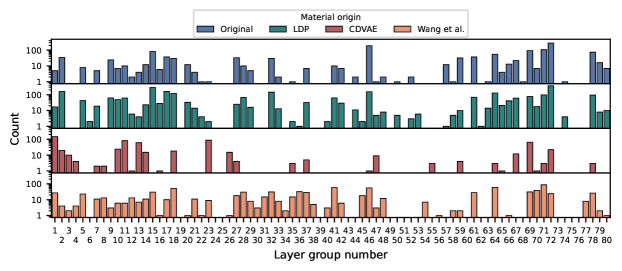
The layer group (the analogue of the space group for a crystal with a 2D lattice) has been determined for all the materials using the algorithm in Ref. Fu et al. (2024). In Fig. 1 we show the histograms of layer group numbers for each of the four sets of materials, namely the original stable materials of the C2DB (original), the materials generated by the deep generative crystal diffusion model (CDVAE), the materials generated by the lattice decoration protocol (LDP), and the materials generated by the symmetry-based approach of Wang et al. (Wang et al.). Note the logarithmic scale. Only materials with formation energies within 0.1 eV/atom of the convex hull are included in the plot.
Not surprisingly, the layer group distribution of the LDP materials is very similar to that of the original materials from which they were generated. The CDVAE structures contain relatively few layer groups while the structures of Wang et al. are more homogeneously distributed and span a larger set of layer groups. No materials are present in the data set for 11 out of the 80 layer groups. These layer groups are: 19, 24, 25, 39, 43, 49, 51, 60, 73, 75, and 76.
II.3 Thermodynamic stability
All the monolayers considered have formation energies within 0.1 eV/atom of the convex hull. In this work we use a convex hull defined by a reference database consisting of the most stable 1,2, and 3-element solid phases from the Open Quantum Materials Database (OQMD)Kirklin et al. (2013) amended by the monolayers themselves (this ensures that the energy above the hull is always non-negative). The threshold value of 0.1 eV/atom has been chosen to account for the finite accuracy of the PBE xc-functional, and to allow for inclusion of meta-stable crystal structures. There are dozens of examples of meta-stable 2D crystal structures that have been experimentally characterised, e.g. the T’-phases of Mo-based dichalcogenides with ranging from 0.18 to 0.02 eV/atom.
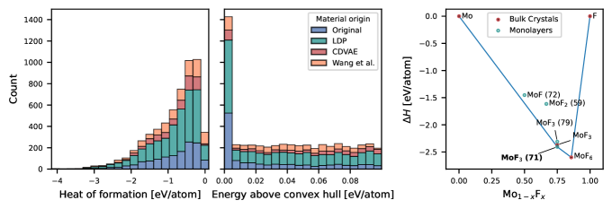
The distribution of heat of formation, , and energy above the convex hull, , for the new materials and stable original materials is shown in Fig. 2. An example of an LDP-generated monolayer on the convex hull ( eV/atom) is MoF3 as seen on the right panel. This monolayer phase has a formation energy of eV/atom below the most stable bulk phase of the same composition. We note that MoF3 does not have a (known) layered bulk counterpart and thus could not have been found by analysing bulk crystal structure databases.
II.4 Dynamical stability
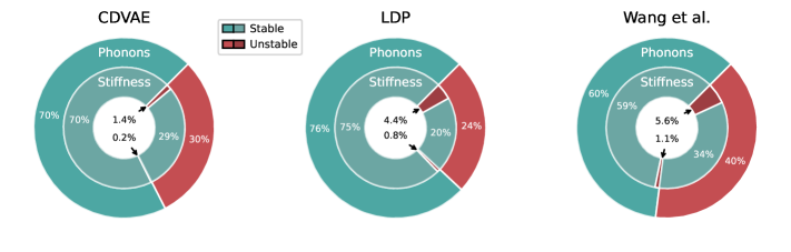
The dynamical stability is assessed by calculating the phonons at the high-symmetry points of the Brillouin zone corresponding to the -points (0,0), (0,0.5), (0.5,0), and (0.5,0.5) in fractional coordinates. An imaginary frequency signals a phonon instability. Moreover, the stiffness tensor is calculated and diagonalized. A negative eigenvalue signals an instability of the shape of the unit cell. A material is termed dynamically stable if all phonon frequencies and stiffness tensor eigenvalues are real and positive. More details including justification of the scheme can be found in Ref. Manti et al. (2023).
Figure 3 shows the distribution of materials according to the dynamical stability (phonons and stiffness, respectively). The materials have been subdivided according to their origin, i.e. LDP, CDVAE, and Wang et al.. For all groups of materials, phonon instabilities occur more frequently than stiffness instabilities. In particular, very few materials that are stable with respect to phonons show stiffness instability (0.2%, 0.8%, and 1.1% for the three groups of materials). A slightly higher percentage (76%) of the LDP materials are found to be dynamically stable with respect to phonons as compared to the CDVAE materials (70%), which in turn have a higher phonon stability rate than the materials from Wang et al. (60%).
The percentage of dynamically stable structures produced by the LDP and CDVAE schemes (70-76%) is similar to that of the subset of seed structures with eV/atom (76%) suggesting that the LDP/CDVAE models learn to generate dynamically stable crystals from the seed/training structures.
In total 2759 of the new materials are found to be dynamically stable. The remaining part of the property workflow is limited to this set of materials.
II.5 Electronic band structure
The electronic band structure has been calculated for all the dynamically stable materials using the PBE xc-functional. For materials with a finite band gap, the band structure has also been obtained with the HSE06 hybrid functional. In both cases spin-orbit coupling (SOC) is included.
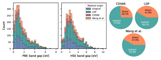
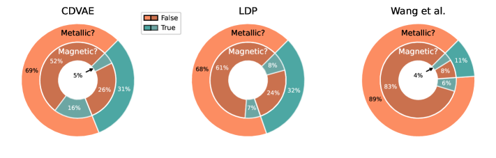
The distribution of the PBE and HSE06 band gaps is shown in Fig. 4 (metals not included). About 30% the new materials generated by LDP and CDVAE are metallic, which is very similar to that of the seed structures (31 %). The fraction of metallic compounds is significantly lower in the set from Wang et al. (11%). Focusing on the 1982 non-metallic compounds, we find that 26% (CDVAE), 42% (LDP), and 47% (Wang) of the new structures have a direct band gap, see pie charts on Fig. 4. Here we classify band gaps as direct if the direct gap is below or within 5 meV of the indirect gap.
Ultra wide band gap materials are important for applications such as insulating dielectrics and ultraviolet photonics. We find 18 new 2D materials with very large band gaps, here defined as the HSE06 band gap exceeding 8 eV. In comparison, the largest band gap in the original set of stable materials in C2DB is 7.49 eV (MgB2H8). 17 of the new large band gap materials are fluorides and most of them have chemical formula XYF6 or YF3, where X is an alkali metal and Y is a transition metal.Only one of the new large band gap materials B4O6 does not contain fluoride.
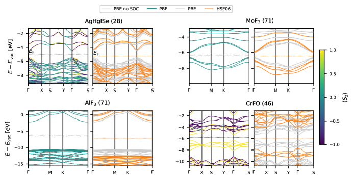
In Fig. 5 we show the PBE and HSE06 band structures for four non-metallic compounds selected from the set of new monolayers: AgHgISe, MoF3, AlF3, and CrFO2. All four materials have a direct band gap.
With a band gap of 10.8 eV (HSE06), AlF3 has the largest band gap among all the new materials. Such large band gap 2D insulators are relevant for several reasons, including as gate dielectrics in field effect transistors employing 2D semiconductors as the channel materialKnobloch et al. (2021); Xu et al. (2023). As an example of a simple, previously unknown monolayer we show the band structure of MoF3. This material lies on the convex hull () and is predicted to have a direct band gap of 1.0 eV (HSE06), which is close to a widely used telecommunication wavelength band (O-band)Cao et al. (2019), making it interesting for photonics and opto-electronic applications in the visible frequency range. As an example of a more complex material we show the band structure of AgHgISe. This material has an energy slightly above the convex hull of ( eV/atom) and a direct band gap of 1.88 eV (HSE06). Finally, as an example of a new magnetic material, we show the band structure of CrFO2. This material also lies on the convex hull and has a direct band gap of 3.65 eV (HSE06).
II.6 Magnetic materials
All the DFT structure relaxations are performed with spin polarisation starting from an initial ferromagnetic spin configuration. If the final structure has absolute magnetic moments on all atoms below , the materials is considered non-magnetic and all subsequent property evaluations are performed on-top of a spin-paired ground state calculation. For magnetic materials, a nearest neighbor exchange coupling, , is derived from the total energy of one specific anti-ferromagnetic configuration. If , the material is classified as ’ferromagnetic’. If , the material is classified as ’magnetic’. Note that in the case of , we do not classify the material as ’anti-ferromagnetic’, because (1) we have only considered one of many possible anti-ferromagnetic configurations and (2) the true magnetic ground state could be more complex, e.g. a spin spiral.
Fig. 6 shows three pie charts depicting the fraction of new materials that are magnetic/non-magnetic and metallic/insulating. Magnetic materials with semiconducting properties are of particular interest for spintronics applications, e.g. spin transistorsDatta and Das (1990). Interestingly, the CDVAE-generated structures contain a significantly larger fraction of magnetic, non-metallic materials (16%) than both the LDP (7%) and Wang et al. (6%) structures.
In addition to the total magnetic moment and the nearest neighbor exchange coupling, the magnetic anisotropy is also calculated by the workflow for materials with one or two magnetic atoms in the unit cell. It represents the total energy difference between spins aligned in the in-plane ( and ) and out-of-plane () directions, respectively. Thus the sign of the magnetic anisotropy determines whether the magnetic material has an easy axis or easy plane.
The magnetic properties of a material can be described using a Heisenberg model (assuming a single magnetic site per unit cell and nearest neighbor interactions)
| (1) |
Here is the nearest neighbor exchange coupling, is the single-ion anisotropy (out-of-plane) and is the anisotropic exchange (out-of-plane). The sums over and is restricted to nearest neighbors. The parameters of the Heisenberg model can be obtained from DFT total energies as described in Ref.Torelli et al. (2019). Using spin wave theory, the spin wave gap, , i.e. the smallest energy required for a magnetic excitation, is given byTorelli et al. (2019)
| (2) |
where is the number of nearest neighbors in the given crystal and is the spin. is required for for out-of-plane magnetism in 2D materials. By combining the exchange coupling and spin wave gap with simple structural parameters, e.g. number of nearest neighbors and lattice type, it is possible to estimate the critical temperature as described in Ref. Torelli et al. (2019). In general for a high critical temperature, both the exchange coupling and the spin wave gap should be as large as possible.
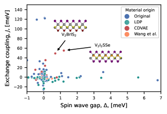
In Fig. 7 the exchange coupling, , is plotted against the spin wave gap, , for the magnetic and non-metallic materials. The two CDVAE generated materials V2I2SSe and V2BrIS2 exhibit notably high values of and . These two share the same crystal structure and belong to layer group 11.
II.7 Dielectric screening
The frequency-dependent 2D optical polarisability, , in the long wave lenght limit (), is calculated within the random phase approximation (RPA). For metals, a Drude term,
| (3) |
is added to the interband polarisability to account for intraband transitions. In this expression the plasma frequency is obtained as an integral of over the Fermi surface, where is a unit vector in the direction of the electric fieldHaastrup et al. (2018)
In materials with a finite band gap, the atomic lattice can also contribute to the polarisability at frequencies below or comparable to the maximum phonon frequency. To include the contribution to the polarisability from infrared (IR) active phonons, we first determine the atomic Born charges describing the change in the macroscopic polarisation, , due to displacement of the atom,
| (4) |
The IR polarisability can then be determined by combining the Born charges with the eigenmodes and frequencies of the optical phonons at the -point. The total polarisability is then obtain as the sum
| (5) |
All quantities in the above equation are tensors.
It has been proposed that the dielectric constant of a layered van der Waals (vdW) bulk crystal can be obtained from the polarisability of its constituent monolayers via the relationsTian et al. (2019)
| (6) | |||||
| (7) |
where is taken as an effective thickness of the 2D material. We estimate as the distance between the two outermost atoms of the monolayer plus the vdW radiiAlvarez (2013) of the outermost atoms. We have checked that this approximation gives a good qualitative agreement with the DFT calculated distance between monolayers in vdW bilayers, albeit slightly underestimating the thicknessPakdel et al. (2023).
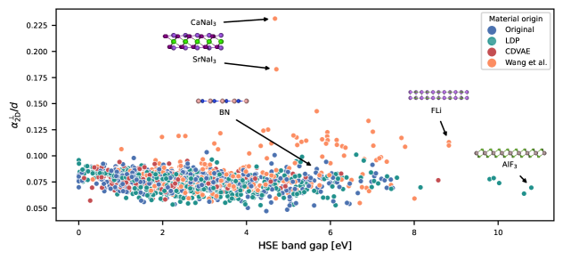
As previously mentioned, 2D vdW materials with good dielectric properties are being actively sought for due to the potential application in 2D electronics, e.g. as gate insulatorsKnobloch et al. (2021); Osanloo et al. (2022); Xu et al. (2023). Good field effect transistor gate dielectrics are characterised by a large electronic band gap (to limit leakage currents) and a large out-of-plane static dielectric constant (to minimise gate thickness and threshold voltage). To screen the new 2D materials for gate dielectric candidates we plot the fraction against the HSE06 band gap, see Fig. 8. While our results show that Eq. (6) is generally quite accurate, we have found that Eq. (7) can lead to a diverging or even negative out-of-plane dielectric constant - even when the layer thickness () is derived from more accurate DFT calculations or experimental interlayer distances. For this reason we show , which directly expresses the ability of the individual 2D layer to screen an electric field. We note in passing that the electronic contribution to the total static polarisability is expected to scale as . While such a trend is indeed observed for the in-plane component () it is almost absent for the out-of-plane component (). These observations agree with previous findingsTian et al. (2019). We ascribe this different behavior to the larger influence of local field effects on the out-of-plane polarisability.
A few of the new materials with particularly large values of the key quantity are highlighted and their atomic structure shown. In particular, CaNaI3 and SrNaI3, which shares structure prototype, have exceptionally high and a reasonably large band gap of 4.4 eV. This is due to a very large phonon contribution to the polarisability, e.g. in the case of CaNaI3, Åwhile Å. Hexagonal BN, which is commonly used in experimental studies, is also highlighted as is AlF3 whose band structure is shown in Fig. 5. In general, the materials from Wang et al. contain several candidates with large phonon contributions to .
II.8 Piezoelectric tensor
The piezoelectric tensor has been calculated for 858 of the new materials that are dynamically stable, non-centrosymmetric, and have a finite band gap.
The piezoelectric tensor, , of an insulating crystal is a rank-3 tensor relating the macroscopic polarization, , to an applied strain. It is non-zero only for crystals lacking an inversion center. In Voigt notation, is expressed as a matrix relating the components of the macroscopic polarizability to the independent components of the strain tensor. The piezoelectric tensor is evaluated as a finite difference of the polarization under three independent strains of the unit cell with the atom positions fully relaxed. The polarisation in the periodic directions is calculated as an integral over Berry phases. The polarization in the non-periodic direction is obtained by direct evaluation of the first moment of the electron density.
For 2D materials, the strain tensor has three independent components comprising two linear ( and ) and one shear () component. Thus strain can be represented as a 3-vector, and the Piezoelectric tensor as a matrix,
| (8) |
where and . As a validation of the computational methodology we mention that the calculated piezoelectric coupling of freestanding MoS2 is 0.35 nC/m in good agreement with the experimental value of 0.3 nC/m. See Ref. Gjerding et al. (2021b) for further details on the computational method.
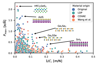
Piezoelectric 2D materials could find applications in nanoscale electro-mechanical devices, mechanical-electrical energy conversion, and sensingZhu et al. (2015); Wu et al. (2014). For a high mechanical-electrical energy conversion, the strain-induced polarisation should be as large as possible, and the elastic energy as small as possible. The strain direction of maximum polarisation is the eigenvector () corresponding to the largest eigenvalue of the matrix . The stiffness of the material in this direction is then . In Fig. 9 we plot the maximum polarisation against the inverse stiffness along the direction of the maximum polarisation for the different materials groups. Some of the materials that look particularly promising mechanical-electrical energy conversion, are highlighted.
II.9 Topological invariants
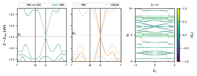
The Berry phase spectrum is calculated for 340 of the new materials with a band gap in the range eV and with less than 13 atoms in the unit cell. The Berry phase spectrum gives the Berry phase, , of an occupied band, , along the path , where a specific point in reciprocal space is given by . The topological indices, in particular the Chern number (), the mirror Chern number (), and the invariant (), can be determined by inspection of the Berry phase spectrum. We refer to Refs. Gjerding et al. (2021a) and Olsen et al. (2019) for more details on the methodology.
An example of a quantum spin Hall insulator is the CDVAE-generated Ta2Te2S. The Berry phase spectrum of this materials is shown in Fig. 10 (right) while the electronic band structures calculated with PBE and HSE06 are shown in the left and middle panels, respectively. From the band structure we note that Ta2Te2S, like grapheneCastro Neto et al. (2009) and siliceneKharadi et al. (2020), hosts a Dirac cone at the K point. However, the band gap of Ta2Te2S (150 meV) is much larger than that of pristine graphene (no gap) and silicene (1.55 meV Liu et al. (2011)), making it more suitable for applications.
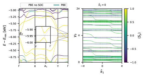
The only example among the new materials of an anomalous Hall insulator is the CDVAE-generated magnetic monolayer Mn2Br2O3. Its Berry phase spectrum and PBE electronic band structure is shown in Fig. 11.
III Summary
We have performed an extensive computational characterisation of 2759 two-dimensional (2D) crystals all of which are predicted to be dynamically and thermodynamically stable, but never have been explored before. Using state of the art ab initio calculations we have determined a variety of basic properties of this previously unknown set materials and made them available in the Computational 2D Materials Database (C2DB). As a result, this work increases the number of stable materials contained in the C2DB by almost a factor of three.
We identify 633 monolayers with a band gap in the semiconductor energy range 0.5-2 eV, of which 156 are direct gaps (results obtained with the HSE06 xc-functional including spin-orbit coupling). We find 406 materials with a magnetic ground state of which 216 have a finite band gap. Among these several exhibit a large magnetic anisotropy, which is an essential requirement for magnetic order at finite temperatures in the 2D limit. In particular, we find a number of semiconducting materials (e.g. the chalcohalides V2BrIS2 and V2I2SSe) with simultaneously large exchange coupling and spin wave gaps making them candidates for 2D magnets with high Curie temperature.
Our calculations provide a complete characterisation of the linear dielectric properties of the non-metallic monolayers. Specifically, both the electronic and phononic contributions to the polarisability are calculated as function of frequency for in-plane and out-of-plane polarisation directions. Focusing on the static out-of-plane polarisability, which is of greatest relevance for dielectric applications in 2D electronics, we identify a number of promising materials combining a high polarisability with a large band gap, e.g. CaNaI3 and SrNaI3. Not surprisingly, these materials are characterised by a relatively large contribution to the polarisability from out-of-plane optical phonons.
The piezoelectric tensor is calculated for more than 800 non-centrosymmetric and insulating monolayers. Based on a combined analysis of the piezoelectric tensor and the stiffness tensor, we identified a number of promising materials for mechanical-electrical energy conversion.
Finally, we have calculated the Berry phase spectrum of 340 materials with small band gaps and used to identify materials with topologically non-trivial band structures. Here we highlighted Ta2Te2S, which we predict to be a quantum spin Hall insulator with a gapped Dirac cone, and Mn2Br2O3, which is classified as a ferromagnetic anomalous Hall insulator.
IV Method
The employed C2DB computational workflow was constructed within the Atomic Simulation Recipes (ASR) Python frameworkGjerding et al. (2021a) and executed using the MyQueueMortensen et al. (2020) task scheduler. The workflow performs calculations using the GPAWEnkovaara et al. (2010) electronic structure code and the Atomic Simulation Environment (ASE) Python libraryLarsen et al. (2017).
All GPAW DFT calculations were performed using an 800 eV plane wave cut-off and a k-point grids with density between 4 and 12 Å. The PBE exchange-correlation functionalPerdew et al. (1996) was used in all calculations, except for the HSE06Heyd et al. (2003) band structure calculations. Spin-orbit coupling was included in calculations of single-particle band energies and the magnetic anisotropy. The precise computational settings used for each type of property calculation can be found in Ref. Gjerding et al. (2021b).
V Data availability
All the crystal structures and their properties are available as a part of C2DB (https://cmr.fysik.dtu.dk/c2db/c2db.html)
VI Acknowledgements
The authors acknowledge funding from the European Research Council (ERC) under the European Union’s Horizon 2020 research and innovation program Grant No. 773122 (LIMA) and Grant agreement No. 951786 (NOMAD CoE). K. S. T. is a Villum Investigator supported by VILLUM FONDEN (grant no. 37789).
VII Competing interests
The authors declare no competing interests.
VIII Author contributions
P.L. and K.S.T. developed the initial concept. P.L. ran the DFT simulations and performed the data analysis. K.S.T. supervised the project and aided with the interpretation of the results. P.L. and K.S.T wrote and discussed the paper together.
References
- Marzari et al. (2021) N. Marzari, A. Ferretti, and C. Wolverton, Nature Materials 20, 736 (2021).
- Thygesen and Jacobsen (2016) K. S. Thygesen and K. W. Jacobsen, Science 354, 180 (2016).
- Saal et al. (2013) J. E. Saal, S. Kirklin, M. Aykol, B. Meredig, and C. Wolverton, JOM 65, 1501 (2013).
- Curtarolo et al. (2012) S. Curtarolo, W. Setyawan, G. L. Hart, M. Jahnatek, R. V. Chepulskii, R. H. Taylor, S. Wang, J. Xue, K. Yang, O. Levy, et al., Computational Materials Science 58, 218 (2012).
- Montavon et al. (2013) G. Montavon, M. Rupp, V. Gobre, A. Vazquez-Mayagoitia, K. Hansen, A. Tkatchenko, K.-R. Müller, and O. A. Von Lilienfeld, New Journal of Physics 15, 095003 (2013).
- Ward et al. (2016) L. Ward, A. Agrawal, A. Choudhary, and C. Wolverton, npj Computational Materials 2, 1 (2016).
- Manti et al. (2023) S. Manti, M. K. Svendsen, N. R. Knøsgaard, P. M. Lyngby, and K. S. Thygesen, npj Computational Materials 9, 33 (2023).
- Wei et al. (2019) J. Wei, X. Chu, X.-Y. Sun, K. Xu, H.-X. Deng, J. Chen, Z. Wei, and M. Lei, InfoMat 1, 338 (2019).
- Mueller et al. (2016) T. Mueller, A. G. Kusne, and R. Ramprasad, Reviews in Computational Chemistry 29, 186 (2016).
- Himanen et al. (2019) L. Himanen, A. Geurts, A. S. Foster, and P. Rinke, Advanced Science 6, 1900808 (2019).
- Schmidt et al. (2019) J. Schmidt, M. R. Marques, S. Botti, and M. A. Marques, npj Computational Materials 5, 83 (2019).
- Knøsgaard and Thygesen (2022) N. R. Knøsgaard and K. S. Thygesen, Nature Communications 13, 468 (2022).
- Merchant et al. (2023) A. Merchant, S. Batzner, S. S. Schoenholz, M. Aykol, G. Cheon, and E. D. Cubuk, Nature 624, 80 (2023).
- Schmidt et al. (2022a) J. Schmidt, H.-C. Wang, T. F. T. Cerqueira, S. Botti, and M. A. L. Marques, Scientific Data 9, 64 (2022a).
- Schmidt et al. (2022b) J. Schmidt, N. Hoffmann, H.-C. Wang, P. Borlido, P. J. M. A. Carriço, T. F. T. Cerqueira, S. Botti, and M. A. L. Marques, “Large-scale machine-learning-assisted exploration of the whole materials space,” (2022b), arXiv:2210.00579 [cond-mat.mtrl-sci] .
- Ashton et al. (2017) M. Ashton, J. Paul, S. B. Sinnott, and R. G. Hennig, Physical Review Letters 118, 106101 (2017).
- Mounet et al. (2018) N. Mounet, M. Gibertini, P. Schwaller, D. Campi, A. Merkys, A. Marrazzo, T. Sohier, I. E. Castelli, A. Cepellotti, G. Pizzi, and N. Marzari, Nature Nanotechnology 13, 246 (2018).
- Haastrup et al. (2018) S. Haastrup, M. Strange, M. Pandey, T. Deilmann, P. S. Schmidt, N. F. Hinsche, M. N. Gjerding, D. Torelli, P. M. Larsen, A. C. Riis-Jensen, et al., 2D Materials 5, 042002 (2018).
- Gjerding et al. (2021a) M. Gjerding, T. Skovhus, A. Rasmussen, F. Bertoldo, A. H. Larsen, J. J. Mortensen, and K. S. Thygesen, Computational Materials Science 199, 110731 (2021a).
- Xie et al. (2021) T. Xie, X. Fu, O.-E. Ganea, R. Barzilay, and T. Jaakkola, arXiv preprint arXiv:2110.06197 (2021).
- Lyngby and Thygesen (2022) P. Lyngby and K. S. Thygesen, npj Computational Materials 8, 232 (2022).
- Wang et al. (2023) H.-C. Wang, J. Schmidt, M. A. L. Marques, L. Wirtz, and A. H. Romero, 2D Materials 10, 035007 (2023).
- Fu et al. (2024) J. Fu, M. Kuisma, A. H. Larsen, K. Shinohara, A. Togo, and K. S. Thygesen, arXiv preprint arXiv:2401.16705 (2024).
- Gjerding et al. (2021b) M. N. Gjerding, A. Taghizadeh, A. Rasmussen, S. Ali, F. Bertoldo, T. Deilmann, N. R. Knøsgaard, M. Kruse, A. H. Larsen, S. Manti, et al., 2D Materials 8, 044002 (2021b).
- Kirklin et al. (2013) S. Kirklin, B. Meredig, and C. Wolverton, Advanced Energy Materials 3, 252 (2013).
- Knobloch et al. (2021) T. Knobloch, Y. Y. Illarionov, F. Ducry, C. Schleich, S. Wachter, K. Watanabe, T. Taniguchi, T. Mueller, M. Waltl, M. Lanza, et al., Nature Electronics 4, 98 (2021).
- Xu et al. (2023) Y. Xu, T. Liu, K. Liu, Y. Zhao, L. Liu, P. Li, A. Nie, L. Liu, J. Yu, X. Feng, et al., Nature Materials 22, 1078 (2023).
- Cao et al. (2019) X. Cao, M. Zopf, and F. Ding, Journal of Semiconductors 40, 071901 (2019).
- Datta and Das (1990) S. Datta and B. Das, Applied Physics Letters 56, 665 (1990).
- Torelli et al. (2019) D. Torelli, K. S. Thygesen, and T. Olsen, 2D Materials 6, 045018 (2019).
- Tian et al. (2019) T. Tian, D. Scullion, D. Hughes, L. H. Li, C.-J. Shih, J. Coleman, M. Chhowalla, and E. J. Santos, Nano Letters 20, 841 (2019).
- Alvarez (2013) S. Alvarez, Dalton Trans. 42, 8617 (2013).
- Pakdel et al. (2023) S. Pakdel, A. Rasmussen, A. Taghizadeh, M. Kruse, T. Olsen, and K. S. Thygesen, arXiv preprint arXiv:2304.01148 (2023).
- Osanloo et al. (2022) M. R. Osanloo, A. Saadat, M. L. Van de Put, A. Laturia, and W. G. Vandenberghe, Nanoscale 14, 157 (2022).
- Zhu et al. (2015) H. Zhu, Y. Wang, J. Xiao, M. Liu, S. Xiong, Z. J. Wong, Z. Ye, Y. Ye, X. Yin, and X. Zhang, Nature Nanotechnology 10, 151 (2015).
- Wu et al. (2014) W. Wu, L. Wang, Y. Li, F. Zhang, L. Lin, S. Niu, D. Chenet, X. Zhang, Y. Hao, T. F. Heinz, et al., Nature 514, 470 (2014).
- Olsen et al. (2019) T. Olsen, E. Andersen, T. Okugawa, D. Torelli, T. Deilmann, and K. S. Thygesen, Phys. Rev. Mater. 3, 024005 (2019).
- Castro Neto et al. (2009) A. H. Castro Neto, F. Guinea, N. M. R. Peres, K. S. Novoselov, and A. K. Geim, Rev. Mod. Phys. 81, 109 (2009).
- Kharadi et al. (2020) M. A. Kharadi, G. F. A. Malik, F. A. Khanday, K. A. Shah, S. Mittal, and B. K. Kaushik, ECS Journal of Solid State Science and Technology 9, 115031 (2020).
- Liu et al. (2011) C.-C. Liu, W. Feng, and Y. Yao, Phys. Rev. Lett. 107, 076802 (2011).
- Mortensen et al. (2020) J. Mortensen, M. Gjerding, and K. Thygesen, The Journal of Open Source Software 5, 1844 (2020).
- Enkovaara et al. (2010) J. Enkovaara, C. Rostgaard, J. J. Mortensen, J. Chen, M. Dułak, L. Ferrighi, J. Gavnholt, C. Glinsvad, V. Haikola, H. Hansen, et al., Journal of Physics: Condensed Matter 22, 253202 (2010).
- Larsen et al. (2017) A. H. Larsen, J. J. Mortensen, J. Blomqvist, I. E. Castelli, R. Christensen, M. Dułak, J. Friis, M. N. Groves, B. Hammer, C. Hargus, et al., Journal of Physics: Condensed Matter 29, 273002 (2017).
- Perdew et al. (1996) J. P. Perdew, K. Burke, and M. Ernzerhof, Physical review letters 77, 3865 (1996).
- Heyd et al. (2003) J. Heyd, G. E. Scuseria, and M. Ernzerhof, The Journal of Chemical Physics 118, 8207 (2003).