Nonconventional screening of Coulomb interaction in two-dimensional semiconductors and metals: A comprehensive cRPA study of MX2 (M=Mo, W, Nb, Ta; X=S, Se, Te)
Abstract
Two-dimensional (2D) semiconducting and metallic transition metal dichalcogenides (TMDs) have attracted significant attention for their promising applications in a variety of fields. Experimental observations of large exciton binding energies and non-hydrogenic Rydberg series in 2D semiconducting TMDs, along with deviations in plasmon dispersion in 2D metallic TMDs, suggest the presence of a nonconventional screening of the Coulomb interaction. The experimentally observed Mott insulating state in the charge density wave (CDW) reconstructed lattice of TMDs containing and elements further confirms the presence of strong Coulomb interactions in these systems. In this study, we use first-principles electronic structure calculations and constrained random-phase approximation to calculate the Coulomb interaction parameters (partially screened and fully screened ) between localized electrons in 2D TMDs. We specifically explore materials represented by the formula MX2 (M=Nb, Ta, Mo, W, and X=S, Se, Te) and consider three different phases (, , and ). Our results show that the short-range interactions are strongly screened in all three phases, whereas the long-range interactions remain significant even in metallic systems. This nonconventional screening provides a compelling explanation for the deviations observed in the usual hydrogenic Rydberg series and conventional plasmon dispersion in 2D semiconducting and metallic TMDs, respectively. Our calculations yield on-site Coulomb interaction parameters within the ranges of 0.8-2.5 eV, 0.8-1.9 eV, and 0.9-2.4 eV for the , , and structures, respectively. These values depend on the specific chalcogen X, the number of electrons, and the correlated subspace. Using the calculated parameters for the undistorted structure, we extract the on-site effective and nearest neighbor Coulomb interaction parameters for reconstructed commensurate CDW NbX2 and TaX2 compounds. Furthermore, our findings indicate a substantially high ratio of on-site effective Coulomb interaction to bandwidth () in CDW TMDs, providing robust evidence for the experimentally observed strongly correlated Mott phase. This work sheds light on the nonconventional screening of Coulomb interactions in 2D TMDs, offering valuable insights into their electronic properties and potential applications in emerging technologies. It advances our fundamental understanding of these materials and holds promise for their use in various applications.
pacs:
73.22.-f, 78.20.Bh, 71.15.-m, 71.10.FdI Introduction
Two-dimensional (2D) transition metal dichalcogenides (TMDs) have attracted significant attention for their unique electronic [1, 2, 3], magnetic [4, 5], optical [6, 7, 8], and valleytronic properties [9, 10, 11, 12]. Semiconducting TMDs have tunable band gaps [13, 14] and high charge carrier mobility, making them promising candidates for next-generation electronic devices that can overcome the limitations of traditional silicon-based technology [15, 16]. TMDs also have strong light-matter interaction and valley-dependent electronic properties, making them ideal for developing valleytronic devices such as valley-selective photodetectors and light-emitting diodes [17, 18, 19]. In addition to their potential applications in optoelectronics and valleytronics, TMDs have also been shown to have promising thermoelectric properties [20, 21, 22, 23]. TMDs have a high thermoelectric figure of merit (), which is a measure of their efficiency as thermoelectric materials. This makes them promising candidates for applications in thermoelectric energy harvesting, waste heat recovery, and refrigeration.
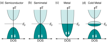
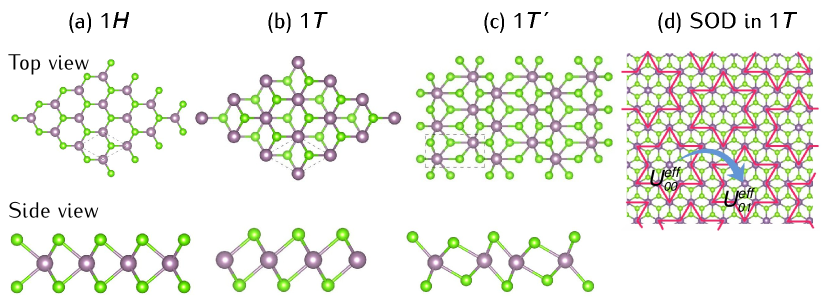
Metallic TMDs, such as ”cold metals” like 1- NbSe2 (see Fig. 1), have opened up new possibilities for device innovation. One notable application is their potential to enable tunnel diodes exhibiting negative differential resistance with ultra-high peak-to-valley current ratios [24]. Cold metallic TMDs have also been shown to achieve sub-60 mV/dec subthreshold swing in CMOS transistors, which could lead to significant improvements in transistor performance [25, 26, 27, 28, 29]. In addition to their applications in nanoelectronics, metallic TMDs exhibit intriguing low-temperature properties such as unconventional plasmon dispersion [30, 31], charge density wave (CDW) phenomena [32, 33, 34], superconductivity [35, 36], and magnetism [37, 38, 39]. These diverse properties are governed by the crystal phases of MX2, which can be trigonal prismatic , octahedral , or distorted octahedral (see Fig. 2) [40, 41]. TMDs are therefore a promising platform for exploring a wide range of phenomena, with the potential to make significant contributions to both fundamental science and technological applications.
The screening of the Coulomb interaction in reduced dimensions is of fundamental interest for practical applications, as it affects the transport and optical properties of low-dimensional devices. In 2D materials containing TM atoms, the dielectric screening of Coulomb interactions is significantly reduced due to the confinement effect and presence of narrow electronic states [42, 43]. This reduced screening has important consequences for the properties of semiconducting TMDs, such as the MoS2 monolayer. For example, it leads to the formation of tightly bound excitons with large binding energies up to 1 eV [44, 45, 46, 47, 48, 49, 50]. Additionally, the exciton excitation spectra in TMDs monolayer strongly deviates from the hydrogenic Rydberg series [51, 52], which indicates a significantly reduced and non-local dielectric screening of the Coulomb interaction. This is further supported by the fact that monolayers of -NbSe2 and -TaS2 are Mott insulators, which is very rare for and transition metal compounds [53]. For metallic 2D TMDs, localized plasmons have been observed experimentally in the correlated 2D CDW -TaSe2 and -NbSe2 materials [54, 30, 31, 55]. Additionally, electron energy-loss spectra (EELS) for these materials have revealed a negative dispersion of the plasmons in these materials [56], which is in contrast to the results for a homogeneous 2D electron gas. This unconventional behavior of the plasmon dispersion is attributed to the electronic correlation effects in these materials.
Monolayer TMDs, especially those with heavy elements like W and Mo have strong spin-orbit coupling and are topological insulators with one-way linear dispersion bands near the Fermi level EF [57, 58]. This crystal phase exhibits an intriguing screening behavior, as electrons in linear bands do not effectively screen long-range Coulomb interactions [59, 60, 61, 62]. This property provides a unique perspective on the interplay between electronic structure and screening phenomena in these materials. Additionally, the topological insulating behavior of TMDs adds another layer of complexity to the interplay of electronic properties and their implications for device applications and emergent physical phenomena.
The study of electronic screening effects and the calculation of Coulomb matrix elements in transition metal (TM) materials, including TMDs, have been the subject of several studies [63, 42, 43, 64]. Most of these studies have focused on TM compounds, which have narrow and states and strong correlation effects. A few works have investigated Coulomb interactions in TMDs with elements [65, 66, 67]. For example, in the distorted structure of TaS2, the on-site Coulomb interaction was calculated to be 0.65 eV [65], which is significantly lower than the value of 2.27 eV for undistorted -TaS2 [66]. Van Loon et al. used first-principles calculations to determine an effective on-site Coulomb interaction eV and a nearest-neighbor interaction eV for -NbS2 [67]. These effective interactions can be incorporated into model Hamiltonians, which can improve the predictive power of model-based calculations. This motivates our systematic and fully ab-initio approach to comprehensively compute effective Coulomb parameters for and TMD monolayers. We anticipate that our work will provide new insights into the complex interplay between electronic structure and interaction effects and that it will enhance the predictive power and applicability of theoretical models in this field.
In this study, we used first-principles electronic structure calculations and constrained random-phase approximation (cRPA) within the full-potential linearized augmented-plane-wave (FLAPW) method to calculate the effective Coulomb interaction parameters between localized electrons in 2D TMDs. We specifically explored materials represented by the formula MX2 (M=Nb, Ta, Mo, W, and X=S, Se, Te) and considered three different phases (, , and ). All compounds in the and phases are metallic, while Mo and W-based compounds in the phases are semiconductors and Nb and Ta-based compounds in the same phase exhibit cold metallic behavior (see Fig. 1 and Table 1). Our results show that the short-range interactions are strongly screened in all three phases, whereas the long-range interaction remains significant even in metallic systems. This nonconventional screening provides a compelling explanation for the deviations observed in the usual hydrogenic Rydberg series and conventional plasmon dispersion in 2D semiconducting and metallic TMDs, respectively. Our calculations yield on-site Coulomb interaction values within the ranges of 0.8-2.5 eV, 0.8-1.9 eV, and 0.9-2.4 eV for the , , and structures, respectively. We find that these values depend on the specific chalcogen X, the number of electrons, and the correlated subspace. Using the calculated parameters for undistorted structure, we extract the on-site effective and nearest neighbor Coulomb interaction parameters for reconstructed commensurate CDW NbX2 and TaX2 compounds. Furthermore, our findings indicate a substantially high ratio of on-site Coulomb interaction to bandwidth () in CDW TMDs, providing robust evidence for the experimentally observed strongly correlated Mott phase. The rest of the manuscript is organized as follows: In Sec. II, we outline the computational method. Sec. III covers results and discussions. Finally, Sec. IV presents conclusions and a summary.
II Computational Method
II.1 Crystal structure and ground state calculations
We consider 2D TMDs, which have the chemical formula MX2. Here, M represents elements such as Mo, W, Nb, and Ta, and X represents chalcogen elements, namely S, Se, and Te. Our study encompasses TMDs with distinct crystallographic structures, including trigonal prismatic (1), octahedral (1), and distorted octahedral (1) structures. The crystal structures are shown in Fig. 2 and the corresponding lattice parameters are given in Table 1. In the 1 and 1 structures, the fundamental unit cell has a hexagonal lattice configuration and it contains one M atom and two X atoms, which are separated by a vacuum region of 20 Å. This is illustrated in Fig. 2(a) and 2(b). For our investigation of the structure, we use an orthorhombic unit cell containing two M atoms and four X atoms, as shown in Fig. 2(c).
| MX2 | Phase | a (Å) | b (Å) | Ground state |
| MoS2 | 3.18 | 3.18 | Semiconductor | |
| 3.19 | 3.19 | Metal | ||
| 5.72 | 3.18 | Semimetal | ||
| MoSe2 | 3.32 | 3.32 | Semiconductor | |
| 3.28 | 3.28 | Metal | ||
| 5.96 | 3.29 | Semimetal | ||
| MoTe2 | 3.55 | 3.55 | Semiconductor | |
| 3.49 | 3.49 | Metal | ||
| 6.36 | 3.46 | Metal | ||
| WS2 | 3.19 | 3.19 | Semiconductor | |
| 3.21 | 3.21 | Metal | ||
| 5.73 | 3.20 | Semimetal | ||
| WSe2 | 3.32 | 3.32 | Semiconductor | |
| 3.29 | 3.29 | Metal | ||
| 5.95 | 3.30 | Semimetal | ||
| WTe2 | 3.55 | 3.55 | Semiconductor | |
| 3.51 | 3.51 | Metal | ||
| 6.31 | 3.49 | Metal | ||
| NbS2 | 3.34 | 3.34 | Cold-metal | |
| 3.38 | 3.38 | Metal | ||
| NbSe2 | 3.47 | 3.47 | Cold-metal | |
| 3.48 | 3.48 | Metal | ||
| NbTe2 | 3.68 | 3.68 | Cold-metal | |
| 3.65 | 3.65 | Metal | ||
| TaS2 | 3.34 | 3.34 | Cold-metal | |
| 3.38 | 3.38 | Metal | ||
| TaSe2 | 3.47 | 3.47 | Cold-metal | |
| 3.50 | 3.50 | Metal | ||
| TaTe2 | 3.70 | 3.70 | Cold-metal | |
| 3.69 | 3.69 | Metal |
The variation in crystal field splitting induced by the neighboring chalcogen X atoms in the three lattice configurations of 1-MX2, 1-MX2, and 1-MX2 yields distinct correlated subspaces, which will be discussed in the following section. This phenomenon plays a key role in expressing the differences in the observed electronic and optical properties of the materials.
In the structure, the chalcogens are aligned vertically along the -axis, with the transition metals sandwiched within the central plane along the -axis. This arrangement results in a Bernal (ABA) stacking configuration, as depicted in the side view of Fig. 2(a). Conversely, the structure exhibits rhombohedral (ABC) stacking, as evident from the side view presented in Fig. 2(b)[69, 70]. In the structure, the orbitals experience a splitting into a singlet , an intermediate-energy doublet (, ), and a high-energy doublet (, ). On the other hand, in the case of the 1 structure, the orbital splits into three lower-energy (, , ) and two higher-energy (, ) states [71].
The 1-MX2 structure of TMDs is a low-symmetry crystal phase that can be considered as a periodically distorted structure of the 1 structure. In the 1 structure, the two adjacent transition metal (TM) atoms move towards each other in the -direction, compared to the 1 structure. The 1 structure is more stable than the 1 structure, and the energy barrier to separate the 1 structure from the stable 1 structure is nearly zero, leading to spontaneous structural distortions [72, 73]. This distortion causes an inversion of the band structure at the point between the orbital of the dichalcogenide and the orbital of the TM, and a cone-like band structure is formed [74, 75].
The FLAPW method, as implemented in the FLEUR code [76], is used for the ground-state calculations. We employ the generalized gradient approximation (GGA) to the exchange-correlation potential, as parametrized by Perdew et al. [77]. To ensure that the results are consistent, calculations are performed using the same cutoff for the wave functions (kmax = 4 a.u.-1), and the same 16 16 1 (12 16 1) -point grid for the 1 and 1 (1) structures in the determination of the ground states. These parameters have been verified to yield well-converged Coulomb interaction parameters across all studied compounds. The maximally localized Wannier functions (MLWFs) are constructed using the WANNIER90 library [78, 79, 80, 81]. The effective Coulomb potential is calculated within the constrained random-phase approximation (cRPA) method [82, 83, 84, 85, 86], as implemented in the SPEX code [87, 88]. We use a 14141 (10141) -point grid for 1 and 1 (1) structures in the cRPA calculations.
II.2 The cRPA method and parametrization of the Coulomb matrix
The cRPA method is an efficient way to calculate the screened Coulomb interaction between localized electrons. It allows us to determine individual Coulomb matrix elements, such as on-site, off-site, intra-orbital, inter-orbital, and exchange, as well as their frequency dependence. The fully screened Coulomb interaction is related to the bare Coulomb interaction by
| (1) |
where is the dielectric function. The dielectric function is related to the electron polarizability by
| (2) |
where the RPA polarization function is given by
| (3) |
Here, are the single-particle DFT Kohn-Sham eigenfunctions, and a positive infinitesimal. with the Kohn-Sham eigenvalues . In the cRPA approach, to exclude the screening due to the correlated subspace, we partition the full polarization function of Eq. (II.2) into two parts.
| (4) |
where includes only the transitions between the states of the correlated subspace and is the remainder. Then, the frequency-dependent effective Coulomb interaction is given schematically by the matrix equation
| (5) |
The set comprises all transitions, excluding those occurring within the correlated subspace The matrix elements of the effective Coulomb interaction in the MLWF basis is given by
| (6) |
where is the MLWF at site with orbital index , and the effective Coulomb potential is calculated within the cRPA method as described above. We define the average on-site diagonal (direct intra-orbital) and off-diagonal (direct and exchange inter-orbital) , matrix elements of the screened Coulomb potential in the static limit as follows [89, 90]:
| (7) |
| (8) |
| (9) |
where is the number of localized orbitals, i.e., one for , three for and five for full orbitals. We employ Eq. (7) to Eq. (9) for all subspaces discussed in this paper. One can show that these Hubbard-Kanamori parameters define the full partially screened Coulomb matrix [Eq. (II.2)] of subspaces formed by and orbitals (assuming spherical symmetry around the atoms). However, to fully define Eq. (II.2) for the three-orbital () and five-orbital () subspaces, we need at least one additional matrix element. For reference, we provide explicit values for several relevant matrix elements in the supplementary material. Similar to the definition of (, ), we can also define the so-called fully screened interaction as well as unscreened (bare) . The bare Coulomb interaction parameter provides information on the localization of Wannier functions. Several procedures have been proposed in the literature to calculate the polarization function for entangled bands [63, 91, 82, 83, 84, 85, 86]. In the present work, we use the method described in Ref. [63, 91].
Calculating Coulomb interaction parameters for the , , and structures is relatively straightforward. However, the star-of-David (SOD) reconstruction increases the number of atoms per 2D unit cell to 39, of which 13 are TM atoms. cRPA calculations for such systems would become very demanding. For the sake of simplicity, we therefore utilize the results from the undistorted structure to make estimations of the on-site and long-range effective Coulomb interactions [66, 92, 65] for the SOD reconstructed systems. The estimated effective Coulomb interaction is given by [65]
| (10) |
when both the vectors and correspond to the positions of TM atoms within a specific star in the 1 structure, represents the on-site effective interaction for that star. On the other hand, to determine the long-range interaction within the reconstructed lattice, vector should pertain to star A, while refers to the indices of TM atoms belonging to the nearest neighboring star B [see a schematic representation of the star of David in Fig. 2(d)].
III Results and discussion
III.1 Correlated subspace
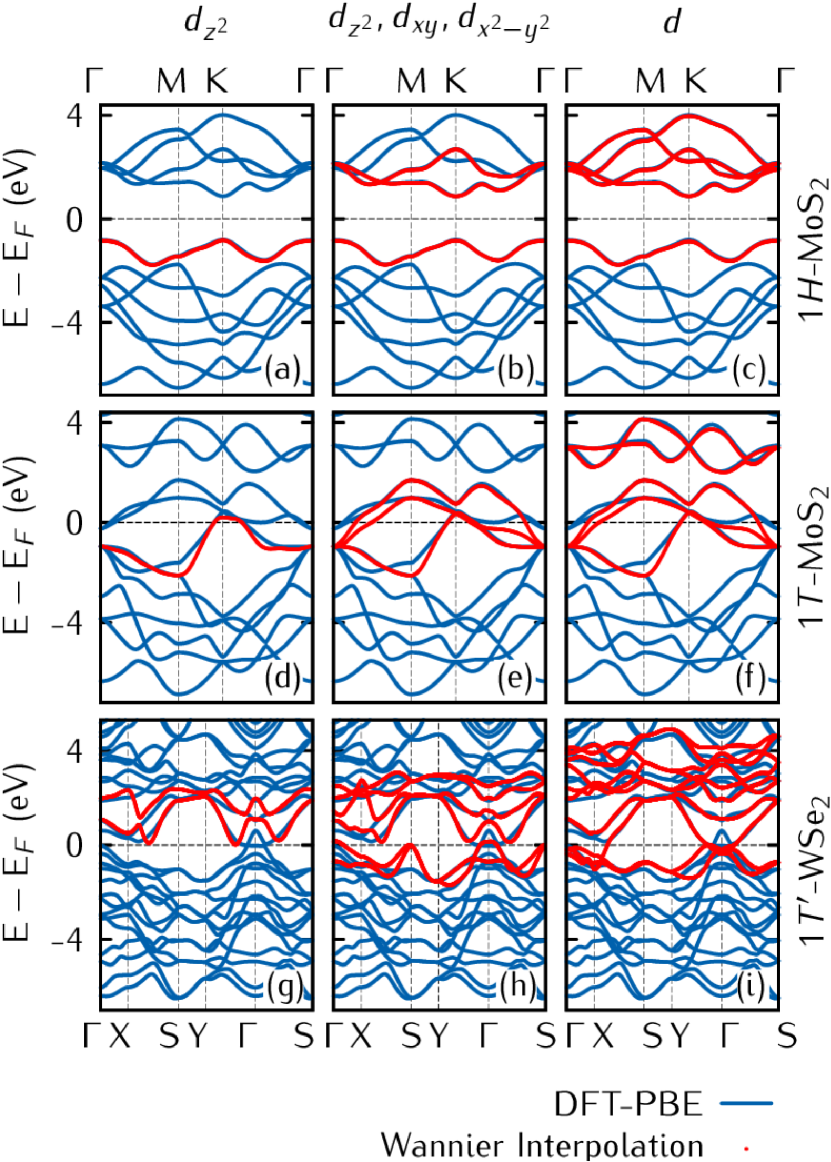
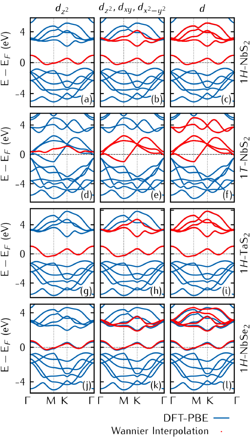
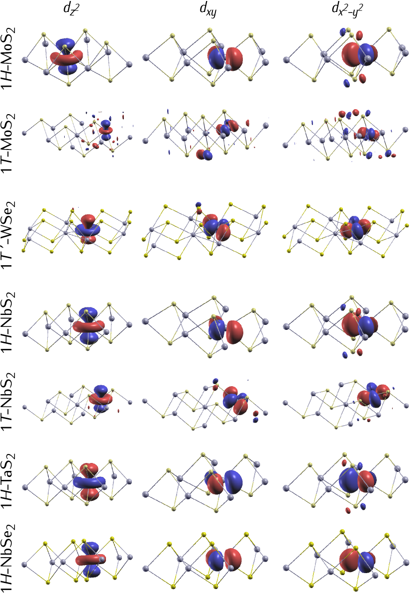
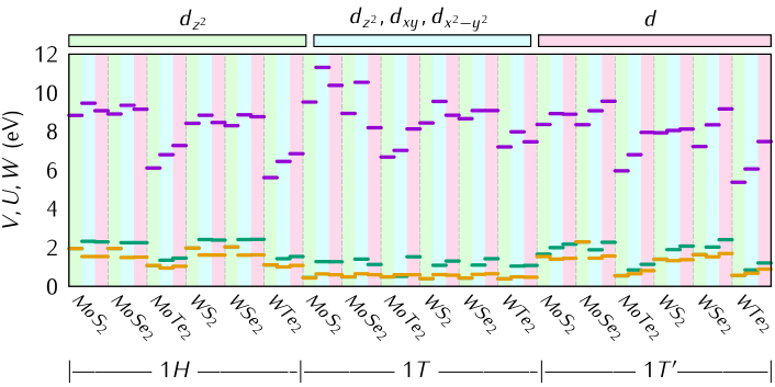
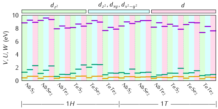
In order to determine the strength of the screened Coulomb interaction, it is important to identify the correlated subspace. This is the subspace of electronic states that are most strongly interacting, and it is essential for the accurate construction of Wannier functions and the corresponding effective low-energy model Hamiltonian. As a first step, we performed electronic structure calculations for all systems. The projected band structures (see Figs. S1 and S2 in supplementary material) show that the orbitals of the TM atom make a significant contribution to the bands near the Fermi level, compared to the other orbitals from chalcogen atoms. Thus, all investigated compounds can be described by an effective low-energy model based on only TM atom electrons. In Fig. 3 and Fig. 4 we compare the DFT-PBE band structures with the corresponding Wannier-interpolated bands for some selected materials. The corresponding Wannier orbitals are depicted in Fig. 5. As seen in Fig. 3, the 1 phase of the MX2 (M=Mo, W; X=S, Se, Te) compounds can be described well by a three-orbital () model, while the 1 and 1 phases of the same materials require a full -orbital effective model. On the other hand, 1 MX2 (M=Nb, Ta; X=S, Se, Te) compounds show cold metallic behavior and thus they can be described by a simple one-orbital model, while the same materials in the 1 structure require a three-orbital model. For consistency, the Coulomb interaction parameters in the following section will be presented for a one-orbital (), for a three-orbital (), and for five-orbital () correlated subspaces.
III.2 Coulomb interaction parameters: MX2 (M=Mo, W; X=S, Se, Te)
Prior to discussing the effective Coulomb interaction parameters in in MX2 (M=Mo, W; X=S, Se, Te) compounds in 1, 1, and 1 structures it is worth noting that the screening of the Coulomb interaction in 2D semiconductors has been extensively explored in recent years by numerous researchers employing various methodologies. For instance, the quantum-electrostatic heterostructure model [93] employs a monopole-dipole approximation to estimate the dielectric function at zero frequency. Trolle et al. [94] proposed a model 2D dielectric function to determine excitonic binding energies. One difficulty in the calculation of dielectric functions of 2D systems with a 3D code is the unwanted but unavoidable screening contribution of the periodic images of the layer in the neighboring supercells. A possible solution is to truncate the Coulomb interaction in the direction [95]. As an alternative, we employ an extrapolation formula that yields the dielectric function for infinite inter-layer distances [96, 97]. The effect of the extrapolation can be seen in Fig. 6. In Fig. S5 of the supplementary material, we show, for reference, the -dependent static dielectric function calculated within RPA for 1H-MoS2 and a layer distance (supercell height) of 25Å, thus including the inter-layer screening. The calculated dielectric function exhibits a behavior similar to the results obtained in other works [95, 98, 99, 100].
The choice of correlated subspace can significantly impact the accuracy of the calculated properties. For example, a minimal three-orbital low-energy model might be sufficient for investigating transport properties in 1 structure, but the inclusion of the full -orbital correlated subspace might be necessary to accurately account for the complex interplay of electrons and photons within the material when delving into optical properties, such as absorption and emission spectra. This distinction highlights the nuanced nature of these materials’ behaviors and the necessity of tailoring the correlated subspace according to the specific properties under investigation. As mentioned in the preceding section, we will consider a one-orbital (), a three-orbital (), and five-orbital () correlated subspace.
| MX2 | Phase | Orbitals | (eV) | (eV) | (eV) | ||
| 8.84 | 1.95 | —– | —– | 1.95 | |||
| 9.47 | 2.33 | 2.04 | 0.15 | 1.54 | |||
| 9.08 | 2.30 | 2.03 | 0.13 | 1.54 | |||
| 9.53 | 0.45 | —– | —– | 0.44 | |||
| 11.32 | 1.28 | 0.96 | 0.17 | 0.64 | |||
| 10.39 | 1.27 | 1.01 | 0.13 | 0.60 | |||
| 8.37 | 1.66 | —– | —– | 1.54 | |||
| 8.93 | 2.00 | 1.57 | 0.22 | 1.41 | |||
| 8.90 | 2.18 | 1.77 | 0.21 | 1.45 | |||
| 8.91 | 1.96 | —– | —– | 1.96 | |||
| 9.36 | 2.26 | 1.98 | 0.16 | 1.49 | |||
| 9.16 | 2.26 | 1.99 | 0.13 | 1.51 | |||
| 8.94 | 0.49 | —– | —– | 0.49 | |||
| 10.55 | 1.41 | 1.06 | 0.18 | 0.65 | |||
| 9.59 | 1.13 | 0.89 | 0.11 | 0.60 | |||
| 8.36 | 2.30 | —– | —– | 2.30 | |||
| 9.08 | 1.89 | 1.43 | 0.21 | 1.46 | |||
| 9.57 | 2.28 | 1.77 | 0.23 | 1.57 | |||
| 6.12 | 1.08 | —– | —– | 1.08 | |||
| 6.81 | 1.35 | 1.18 | 0.08 | 0.95 | |||
| 7.28 | 1.46 | 1.25 | 0.09 | 1.04 | |||
| 6.69 | 0.49 | —– | —– | 0.49 | |||
| 7.03 | 0.52 | 0.35 | 0.07 | 0.60 | |||
| 8.14 | 1.53 | 1.31 | 0.11 | 0.60 | |||
| 5.97 | 0.55 | —– | —– | 0.55 | |||
| 6.81 | 0.85 | 0.56 | 0.15 | 0.65 | |||
| 7.96 | 1.14 | 0.78 | 0.18 | 0.81 | |||
| 8.43 | 1.98 | —– | —– | 1.98 | |||
| 8.85 | 2.42 | 2.16 | 0.15 | 1.62 | |||
| 8.47 | 2.39 | 2.14 | 0.12 | 1.62 | |||
| 8.45 | 0.40 | —– | —– | 0.40 | |||
| 9.56 | 1.09 | 0.85 | 0.13 | 0.61 | |||
| 8.85 | 1.31 | 1.09 | 0.12 | 0.58 | |||
| 7.94 | 1.40 | —– | —– | 1.40 | |||
| 8.06 | 1.90 | 1.51 | 0.21 | 1.33 | |||
| 8.13 | 2.08 | 1.70 | 0.20 | 1.38 | |||
| 8.31 | 2.04 | —– | —– | 2.04 | |||
| 8.87 | 2.42 | 2.16 | 0.17 | 1.61 | |||
| 8.77 | 2.43 | 2.16 | 0.14 | 1.63 | |||
| 8.67 | 0.43 | —– | —– | 0.43 | |||
| 9.09 | 1.10 | 0.84 | 0.15 | 0.62 | |||
| 9.09 | 1.43 | 1.15 | 0.14 | 0.65 | |||
| 7.23 | 1.64 | —– | —– | 1.64 | |||
| 8.35 | 2.03 | 1.59 | 0.21 | 1.53 | |||
| 9.17 | 2.41 | 1.88 | 0.23 | 1.70 | |||
| 5.62 | 1.11 | —– | —– | 1.11 | |||
| 6.46 | 1.43 | 1.26 | 0.09 | 1.00 | |||
| 6.86 | 1.54 | 1.33 | 0.09 | 1.08 | |||
| 7.21 | 0.39 | —– | —– | 0.39 | |||
| 7.99 | 1.05 | 0.84 | 0.14 | 0.49 | |||
| 7.47 | 1.08 | 0.89 | 0.11 | 0.47 | |||
| 5.38 | 0.57 | —– | —– | 0.57 | |||
| 6.07 | 0.85 | 0.59 | 0.12 | 0.68 | |||
| 7.49 | 1.21 | 0.85 | 0.17 | 0.89 |
In Table 2, we present on-site Coulomb interaction parameters, including the bare , the partially screened Hubbard-Kanamori parameters , , and , as well as the fully screened . Note that the definitions of and are the same as , i.e., the average diagonal elements of the Coulomb matrix [see Eq.(7)]. To facilitate a more comprehensive comparison, we visualize the unscreened , partially screened , and fully screened parameters across all compounds and their corresponding phases. This graphical representation is presented in Fig. 7, enhancing our ability to discern the variations and trends in these interactions more effectively.
Let us begin with a discussion of the bare (unscreened) Coulomb interaction. The bare values range from 5.6 to 11.3 eV and depend on the principal quantum number of the shell, chalcogen X, and symmetry of the structure. Our calculated interaction for M=Mo and W with and orbitals, respectively, are almost 4-5 eV smaller than the bare Coulomb interactions of TMDs with correlated subspaces [42]. Additionally, if we focus on a specific subspace, the calculated parameters for WX2 are smaller than MoX2. This is not unexpected, as the bare interaction generally decreases when moving downward in the periodic table from TM to TM materials, due to the lower degree of contraction of the wave functions compared to and ones. Furthermore, the results for the chalcogen series MX2 with X=S to Te tend to show a reduction in bare (with exceptions). One might attribute this to the increase in the lattice constant, making the Wannier function more extended or more delocalized. This can be seen in Fig. 5, which shows the shape of Wannier orbitals for Mo(W)X2 compounds. An analysis of the shape of these Wannier functions and the projected band structures (see supplementary material) indicates that the coupling of states to neighboring chalcogen states is not negligible, which leads to delocalization and, therefore, to smaller bare interaction parameters in X=Se, Te compounds compared to X=S. From a symmetry point of view, the largest value of bare interaction is observed in the structure. This is consistent with the stronger contraction of wave functions and weaker admixture of chalcogen with states in the structure.
In most of the TMDs considered, the Coulomb interaction is screened efficiently due to the high density of M- and X- states near the Fermi level . As a consequence, the on-site and values are considerably reduced. The calculated values for -MX2, -MX2, and -MX2 lie in the range 1.3-2.4 eV, 1.1-1.4 eV, and 0.9-2.4 eV, respectively. The calculated and values depend on the correlated subspace, ground-state electronic structure, and chalcogen X atom. In contrast to the bare interaction, the values are larger in the structure. This can be attributed to the band gap of the materials in this structure. For example, considering a three-orbital correlated subspace, the values in the structure are smaller than in and due to a metallic screening channel stemming from the chalcogen X- states in the and structures (see Fig. 3 and the projected band structure in the supplementary material).
| MX2 | Phase | Orbitals | (eV) | (eV) | (eV) | (eV) | (eV) | (eV) | (eV) |
| 1.95 | 1.08 | 0.84 | 0.78 | 0.66 | 0.60 | 0.54 | |||
| 2.33 | 1.29 | 1.01 | 0.93 | 0.79 | 0.72 | 0.65 | |||
| 2.30 | 1.29 | 1.01 | 0.93 | 0.79 | 0.72 | 0.65 | |||
| 0.45 | 0.09 | 0.03 | 0.02 | 0.01 | 0.01 | 0.00 | |||
| 1.28 | 0.26 | 0.09 | 0.07 | 0.03 | 0.02 | 0.01 | |||
| 1.27 | 0.27 | 0.10 | 0.07 | 0.02 | 0.01 | 0.00 | |||
| 1.66 | 0.94 | 0.89 | 0.71 | 0.71 | 0.67 | 0.59 | |||
| 2.00 | 1.13 | 1.08 | 0.86 | 0.85 | 0.81 | 0.71 | |||
| 2.18 | 1.24 | 1.16 | 0.93 | 0.91 | 0.87 | 0.76 | |||
| 1.96 | 1.08 | 0.86 | 0.80 | 0.68 | 0.63 | 0.56 | |||
| 2.26 | 1.25 | 0.99 | 0.92 | 0.78 | 0.72 | 0.65 | |||
| 2.26 | 1.25 | 0.99 | 0.92 | 0.78 | 0.72 | 0.65 | |||
| 0.49 | 0.11 | 0.05 | 0.04 | 0.02 | 0.01 | 0.00 | |||
| 1.41 | 0.33 | 0.15 | 0.11 | 0.05 | 0.03 | 0.01 | |||
| 1.13 | 0.36 | 0.17 | 0.12 | 0.05 | 0.03 | 0.01 | |||
| 2.30 | 1.29 | 1.25 | 0.99 | 1.01 | 0.94 | 0.83 | |||
| 1.89 | 1.06 | 1.03 | 0.81 | 0.83 | 0.77 | 0.69 | |||
| 2.28 | 1.24 | 1.18 | 0.94 | 0.93 | 0.88 | 0.77 | |||
| 1.08 | 0.69 | 0.55 | 0.52 | 0.44 | 0.41 | 0.37 | |||
| 1.35 | 0.86 | 0.69 | 0.64 | 0.55 | 0.51 | 0.46 | |||
| 1.46 | 0.84 | 0.69 | 0.64 | 0.55 | 0.51 | 0.46 | |||
| 0.49 | 0.21 | 0.17 | 0.17 | 0.15 | 0.14 | 0.13 | |||
| 0.52 | 0.22 | 0.19 | 0.18 | 0.16 | 0.15 | 0.14 | |||
| 1.53 | 0.82 | 0.66 | 0.62 | 0.53 | 0.49 | 0.44 | |||
| 0.55 | 0.17 | 0.16 | 0.10 | 0.09 | 0.09 | 0.07 | |||
| 0.85 | 0.27 | 0.25 | 0.16 | 0.13 | 0.15 | 0.10 | |||
| 1.14 | 0.32 | 0.28 | 0.17 | 0.14 | 0.15 | 0.10 | |||
| 1.98 | 1.13 | 0.88 | 0.81 | 0.68 | 0.62 | 0.56 | |||
| 2.42 | 1.38 | 1.07 | 0.99 | 0.83 | 0.76 | 0.68 | |||
| 2.39 | 1.38 | 1.07 | 0.99 | 0.83 | 0.76 | 0.68 | |||
| 0.40 | 0.09 | 0.04 | 0.03 | 0.01 | 0.01 | 0.01 | |||
| 1.09 | 0.25 | 0.10 | 0.08 | 0.04 | 0.02 | 0.01 | |||
| 1.31 | 0.40 | 0.18 | 0.14 | 0.05 | 0.03 | 0.00 | |||
| 1.40 | 0.77 | 0.73 | 0.58 | 0.56 | 0.55 | 0.47 | |||
| 1.90 | 1.04 | 0.99 | 0.79 | 0.76 | 0.74 | 0.64 | |||
| 2.08 | 1.14 | 1.06 | 0.86 | 0.81 | 0.80 | 0.68 | |||
| 2.04 | 1.14 | 0.90 | 0.84 | 0.71 | 0.65 | 0.58 | |||
| 2.42 | 1.36 | 1.07 | 0.99 | 0.84 | 0.77 | 0.69 | |||
| 2.43 | 1.35 | 1.07 | 0.99 | 0.84 | 0.77 | 0.69 | |||
| 0.43 | 0.09 | 0.04 | 0.03 | 0.02 | 0.01 | 0.01 | |||
| 1.10 | 0.24 | 0.10 | 0.08 | 0.04 | 0.03 | 0.01 | |||
| 1.43 | 0.39 | 0.18 | 0.13 | 0.05 | 0.03 | 0.00 | |||
| 1.64 | 0.95 | 0.92 | 0.74 | 0.73 | 0.70 | 0.61 | |||
| 2.03 | 1.18 | 1.14 | 0.91 | 0.91 | 0.86 | 0.76 | |||
| 2.41 | 1.31 | 1.24 | 0.99 | 0.97 | 0.93 | 0.81 | |||
| 1.11 | 0.72 | 0.58 | 0.54 | 0.46 | 0.42 | 0.38 | |||
| 1.43 | 0.93 | 0.74 | 0.69 | 0.59 | 0.54 | 0.48 | |||
| 1.54 | 0.91 | 0.74 | 0.69 | 0.59 | 0.54 | 0.48 | |||
| 0.39 | 0.12 | 0.06 | 0.05 | 0.03 | 0.02 | 0.01 | |||
| 1.05 | 0.32 | 0.17 | 0.14 | 0.07 | 0.04 | 0.02 | |||
| 1.08 | 0.36 | 0.19 | 0.15 | 0.08 | 0.05 | 0.02 | |||
| 0.57 | 0.21 | 0.20 | 0.12 | 0.11 | 0.11 | 0.08 | |||
| 0.85 | 0.31 | 0.29 | 0.18 | 0.16 | 0.17 | 0.12 | |||
| 1.21 | 0.37 | 0.33 | 0.20 | 0.17 | 0.17 | 0.11 |
In the structure, all states are split due to its lower symmetry compared to the structure, which significantly modifies the electronic structure [101]. In this context, the full orbital set is the optimal correlated subspace for capturing the electronic characteristics of this structure. The semimetallic behavior of the structure enhances electron-electron interactions compared to the structure [102, 103, 101, 104]. While the structure does not have a band gap, the scarcity of metallic states near the Fermi level reduces the contribution of X- M- transitions to screening, resulting in a value that is largely similar to that of the structure.
Regardless of the correlated subspace or structural symmetry, electron screening is enhanced in the MTe2 compared to MS2/MSe2, leading to a reduction in both the Coulomb interaction parameters and . For example, in the three-orbital correlated subspace, the value decreases from 2.33 eV in -MoS2 to 1.35 eV in -MoTe2. The transition from S to Te in each MX2 system contributes to the determination of the and parameters through two mechanisms. First, similar to the effect seen in the bare interaction, the Wannier localization effect causes a reduction in and from S to Te. Second, the shift from S/Se to Te brings the X- states into closer energy proximity with the M- states, as shown in Fig. S1 of the supplementary material. This closeness in energy levels translates to a smaller energy difference, which increases the contribution of X- M- transitions to the polarization function and as a consequence reduces the and parameters. On the other hand, a comparison of MoX2 and WX2 compounds reveals that the screened interactions are nearly identical for most of them. This is likely due to the similar atomic radii of Mo and W, which leads to a similar degree of localization of the orbitals in both materials.
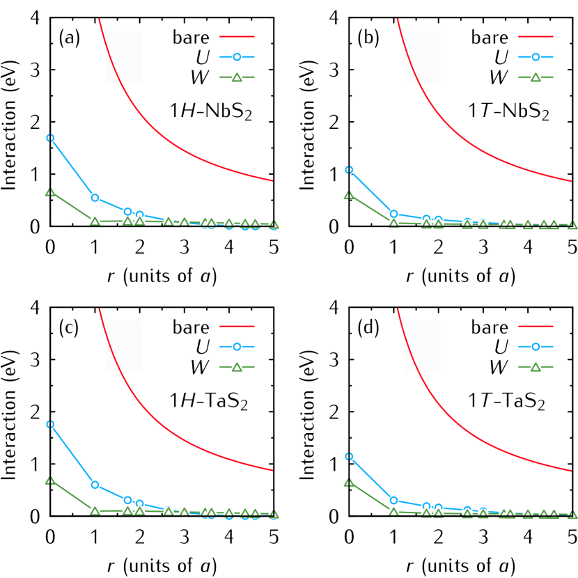
So far, we have only considered the on-site Coulomb interaction matrix elements. The long-range off-site Coulomb interaction plays an important role in determining the phase diagram of 2D materials. The long-range behavior of the screened Coulomb interaction is shown in Fig. 8 for four MX2 compounds and compared with the unscreened interaction. Table 3 reports the off-site partially screened Coulomb interaction for all considered Mo- and W-based TMDs as a function of distance up to . As shown in Fig. 8(a), the effective Coulomb interaction in -MoS2 reveals a significant long-range part of . This indicates that the short-range interaction is strongly screened, while the long-range interaction is weakly screened. Furthermore, due to reduced screening at large distances, in -MoS2 the calculated approaches the bare interaction . The metallic states in the structure [see Fig. 8(c)] give rise to a significant reduction in long-range Coulomb interaction, and it is fully screened at a short distance of about 1.5a. In contrast, for the -MoS2 it takes a considerably larger value at a short distance. We find that the ratio for -MoS2 has a strong -dependence, i.e., =3.4, =2.1, =1.7, where the distance is given in units of lattice constant . This means that the -dependent screening in -MX2 deviates substantially from , i.e., and cannot be expressed by a simple static dielectric constant . The situation is quite similar in other considered TMDs with structure, where the dielectric constant decreases with distance, in agreement with recent experiments. This -dependent nonconventional screening explains the large exciton binding energies and deviations from the usual hydrogenic Rydberg series of energy levels of the excitonic states in semiconducting monolayer TMDs [51, 52]. Note that the long-range behavior of the for bulk MoS2 can be fitted by a static dielectric constant (see Fig. S3 in supplementary material), revealing a conventional screening in three-dimensional semiconductors. Indeed, the dielectric constant that we use is very close to the experimental value of [105].
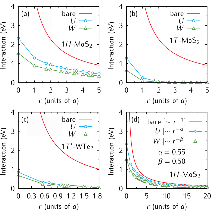
Most monolayer MoX2 and WX2 materials are stable only in the structure. However, recent work has shown that monolayer of WSe2 can also be grown in the structure, which has a topological gap of 129 meV as measured by angle-resolved photoemission spectroscopy (ARPES) experiments [57, 58]. In the absence of spin-orbit coupling, -WX2 is a semimetal, with two bands meeting at the Fermi level (EF), similar to graphene. However, the valence band maximum in -WX2 has a flattened non-parabolic shape along the -Y direction, while the conduction and valence bands in graphene meet at the K point with linear dispersion. From the point of view of screening, electrons in linear bands behave like electrons in an insulator, and the long-range part of the effective Coulomb interaction is not screened well [60, 59, 106]. In the structure of MX2 compounds, the screening also turns out to be non-local, even though the bands do not have purely linear dispersion. For example, in the full subspace of MoS2, the non-local sixth neighbor interaction for the structure is 0.76 eV, which is even larger than the corresponding value for the semiconducting structure ( = 0.65 eV). These findings have important implications for our understanding of the interaction effects in 2D materials. It suggests that the relationship between long-range screening and linear dispersion is not straightforward and that other factors such as the density of correlated states around EF and the overlap of the orbitals with these states also play a role.
III.3 Coulomb interaction parameters: MX2 (M=Nb, Ta; X=S, Se, Te)
The 2D Mo(W)X2 compounds discussed in the preceding section can have different ground states, ranging from semiconducting to semimetallic to metallic, depending on the crystal structure. In this section, we investigate the screening of the Coulomb interaction in Nb- and Ta-based MX2 compounds (where X=S, Se, Te). Nb and Ta atoms have one fewer electron than Mo and W atoms. Their electronic structures show different metallic behaviors. In the structure, these materials show cold metallic behavior, while in the structure they are normal metals (see Fig. 1 and Fig. 4 ). As can be seen from the Wannier interpolated band structures in Fig. 4 a minimal one-orbital low-energy model may be sufficient for investigating transport properties in the structure of these materials. However, the structure requires a more comprehensive three-orbital low-energy model. For completeness, we provide Coulomb interaction parameters for three correlated subspaces: a single orbital (), a three-orbitals ( + + ), and the full shell of the TM atom. The calculated Coulomb interaction parameters, including the bare , Hubbard-Kanamori parameters (, , and ), and the fully screened , are systematically presented in Table 4 and Fig. 9 provides a visual representation of the trends of , , and parameters across all compounds and their respective phases, to facilitate the comparison.
| MX2 | Phase | Orbitals | (eV) | (eV) | (eV) | ||
| 8.84 | 1.29 | —– | —– | 0.43 | |||
| 9.25 | 1.69 | 1.39 | 0.15 | 0.67 | |||
| 8.92 | 2.30 | 2.01 | 0.13 | 0.67 | |||
| 8.36 | 1.23 | —– | —– | 0.41 | |||
| 8.99 | 1.08 | 0.83 | 0.14 | 0.61 | |||
| 8.74 | 1.77 | 1.52 | 0.13 | 0.61 | |||
| 9.21 | 1.11 | —– | —– | 0.37 | |||
| 9.58 | 1.59 | 1.29 | 0.17 | 0.62 | |||
| 9.35 | 2.25 | 1.97 | 0.14 | 0.64 | |||
| 9.01 | 1.16 | —– | —– | 0.52 | |||
| 9.19 | 1.25 | 0.96 | 0.16 | 0.56 | |||
| 9.19 | 1.29 | 1.03 | 0.14 | 0.58 | |||
| 7.93 | 0.65 | —– | —– | 0.36 | |||
| 8.36 | 0.96 | 0.71 | 0.12 | 0.49 | |||
| 8.05 | 0.94 | 0.70 | 0.10 | 0.49 | |||
| 8.18 | 0.60 | —– | —– | 0.35 | |||
| 8.86 | 0.86 | 0.59 | 0.13 | 0.53 | |||
| 8.30 | 0.93 | 0.70 | 0.11 | 0.50 | |||
| 8.12 | 1.13 | —– | —– | 0.41 | |||
| 8.66 | 1.76 | 1.47 | 0.16 | 0.69 | |||
| 8.34 | 2.40 | 2.12 | 0.12 | 0.70 | |||
| 8.63 | 1.15 | —– | —– | 0.46 | |||
| 8.35 | 1.14 | 0.90 | 0.14 | 0.65 | |||
| 7.87 | 1.89 | 1.66 | 0.12 | 0.61 | |||
| 8.74 | 2.05 | —– | —– | 0.45 | |||
| 9.19 | 2.47 | 2.18 | 0.19 | 0.67 | |||
| 8.96 | 2.45 | 2.17 | 0.14 | 0.69 | |||
| 8.58 | 1.14 | —– | —– | 0.38 | |||
| 8.90 | 1.21 | 0.95 | 0.16 | 0.62 | |||
| 8.85 | 1.52 | 1.26 | 0.14 | 0.64 | |||
| 7.67 | 0.90 | —– | —– | 0.33 | |||
| 8.15 | 1.17 | 0.92 | 0.15 | 0.52 | |||
| 7.88 | 1.14 | 0.88 | 0.11 | 0.53 | |||
| 7.36 | 0.78 | —– | —– | 0.30 | |||
| 8.29 | 0.87 | 0.61 | 0.12 | 0.54 | |||
| 7.62 | 0.94 | 0.72 | 0.11 | 0.50 |
We find that the calculated parameters are slightly smaller than the same parameters in Mo(W)X2 compounds. This is because the Nb (Ta) atom has one electron less than the Mo (W) atom (less nuclear charge), and thus the wave functions are less contracted, leading to less localized Wannier functions and as a consequence slightly smaller parameters. This is consistent with the findings of previous studies [63, 42, 107]. We also compare the parameters in Nb(Ta)X2 compounds with the corresponding ones in elementary transition metals. We find that the values for the considered 4/5 TMDs compounds, namely NbX2 and TaX2, are almost 2 eV smaller than the corresponding ones in elementary Nb or Ta bulk systems [63]. This is likely due to the coupling to neighboring chalcogen states in TMDs. The coupling to states makes the TM orbitals spill into the states, giving rise to delocalization and, therefore, to smaller parameters. This effect is also reflected in the shape of the Wannier orbitals shown in Fig. 5 and in the projected band structures (see supplementary material). An analysis of the shape of the Wannier orbitals reveals that for any system in which the overlap of the and orbitals is stronger, the Wannier functions spread to the nearest neighboring atoms. Moreover as shown in Fig. S4, the coupling to neighboring chalcogen states gets stronger in Te-based TMDs, which makes the Wannier functions more extended.
Similarly to the bare Coulomb interaction parameters discussed above, the Wannier localization effect is also important for the partially screened and fully screened parameters. The () parameter tends to decrease from Mo/W to Nb/Ta TMDs systems because the Wannier functions are less localized in Nb/Ta TMDs due to smaller value of nuclear charge. In addition, for the structure of MX2 (M=Nb, Ta), a flat half-filled band with mainly character increases screening substantially. This results in larger and differences compared to the corresponding differences for the -MX2 (M=Mo, W) compounds. Note that although the interaction parameter is smaller in metallic MX2 (M=Nb, Ta) compounds than in elementary TMs and other materials containing transition metals, such as MXenes ( eV) [64], the narrow bands with , , and character in TMDs result in a larger correlation strength.
Strong interactions between localized electrons can lead to a transition from a metal to an insulator and trigger a magnetic phase change [37, 38, 108, 109]. Magnetic ordering and Mott phases have been experimentally observed in layered materials containing transition metal (TM) atoms, such as the TM halides CrI3 [110, 111], VI3 [112, 43], the 3d transition metal dichalcogenides (TMDs) -VX2 [113, 42], and the TM phosphorous trichalcogenides NiPX3 (where X=S and Se) [114]. All of these materials have flat bands in their energy spectra. In the case of -NbX2 and -TaX2, there is an isolated, half-filled low-energy band with predominantly character resulting in a large ratio. Although the structure of NbX2 and TaX2 has stronger correlations due to a single, narrow band, Mott-like insulating behavior has been observed in the reconstructed lattice.
Experimentally, compounds such as TaS2[115], NbSe2 [116], and TaSe2 [117] exhibit metallic behavior at high temperatures in the 1 crystal structure. However, as the temperature is lowered, they undergo a transition to an insulating phase characterized by a distinct atomic rearrangement pattern, known as the ”star-of-David” motif [118, 119, 120, 121]. For example, the reconstructed 1-TaS2 monolayer has a Mott gap of 0.45 eV [108]. This lattice reconstruction coincides with a commensurate CDW (CCDW) transition.
| MX2 | Phase | Orbitals | (eV) | (eV) |
| NbS2 | 0.71 | 0.40 | ||
| NbSe2 | 0.27 | 0.06 | ||
| NbTe2 | 0.18 | 0.04 | ||
| TaS2 | 0.83 | 0.47 | ||
| TaSe2 | 0.35 | 0.07 | ||
| TaTe2 | 0.18 | 0.04 |
The effective Coulomb interaction for the star-of-David configuration in MX2 lattices has been reported in the literature by some authors [66, 92, 65]. Following the same procedure [see Eq.(10)] and using the results of the undistorted 1 structure, we estimated the on-site and off-site Coulomb interactions. The results are presented in Table 5. In the cases of NbS2 and TaS2, we obtain values of 0.71 eV and 0.83 eV, respectively. This is 0.18 eV larger than the value of 0.65 eV reported for TaS2 in a previous study using the same approach [65]. The on-site interaction is large enough compared to the bandwidth =0.02 eV [66, 65] which induces a robust Mott insulator in CCDW 1-TaS2. Moreover, for TaSe2 is also sizable, revealing the importance of the correlation in other MX2 which have not been quantitatively studied before.
The stabilization of the distorted CCDW 1-MX2 (M=Nb, Ta) not only increases the ratio of the on-site effective Coulomb interaction to the bandwidth , but also leads to an increase in the ratio of the long-range interaction to up to 0.56. This could potentially lead to the emergence of exotic quantum phenomena. The obtained on-site and off-site Coulomb interaction parameters are important for use in extended model Hamiltonians and methods beyond DFT, such as DFT+ and DFT plus dynamical mean-field theory (DFT+DMFT), which is used to obtain a reliable electronic structure, Mott gap, and other properties.
We have discussed the on-site Coulomb interaction parameters in Nb(Ta)X2 (where X=S, Se, Te) compounds. As in Mo(W)X2 compounds, the screening of the long-range Coulomb interaction is nonconventional in these compounds. Figure 10 shows the calculated partially and fully screened Coulomb interaction parameters and for the and phases of NbS2 and TaS2 compounds as a function of distance up to . Despite the metallic nature of these compounds, the long-range Coulomb interactions do not screen well, and as a consequence, long-range interactions remain sizable, as shown in Table 6. The important consequence of this reduced screening and sizable long-range Coulomb interaction in metallic systems is the appearance of CDW order and the existence of intriguing plasmons in TMDs. The latter will be discussed in detail below. Note that CDW appears to be stronger in the single-layer form of 1-MX2 [122, 32, 33, 34]. The sizable in the 1 structure indicates that the electron-electron interaction is one of the main reasons for the occurrence of CDW order in TMDs. Although the value of off-site in the 1 structure is not negligible, it is not as large as the corresponding one in the 1 structure. It would be interesting to take off-site into account within the extended Hubbard model and investigate whether CDW order occurs for TaX2 and NbX2 or not.
| MX2 | Phase | Orbitals | (eV) | (eV) | (eV) | ||||
| 1.29 | 0.42 | 0.22 | 0.17 | 0.09 | 0.06 | 0.03 | |||
| 1.69 | 0.55 | 0.28 | 0.22 | 0.11 | 0.07 | 0.03 | |||
| 2.30 | 1.23 | 0.97 | 0.90 | 0.76 | 0.69 | 0.62 | |||
| 1.23 | 0.27 | 0.16 | 0.14 | 0.10 | 0.08 | 0.06 | |||
| 1.08 | 0.24 | 0.14 | 0.13 | 0.09 | 0.07 | 0.05 | |||
| 1.77 | 0.79 | 0.61 | 0.57 | 0.48 | 0.45 | 0.40 | |||
| 1.11 | 0.34 | 0.17 | 0.14 | 0.07 | 0.05 | 0.02 | |||
| 1.59 | 0.48 | 0.25 | 0.20 | 0.10 | 0.06 | 0.03 | |||
| 2.25 | 1.19 | 0.95 | 0.89 | 0.76 | 0.70 | 0.63 | |||
| 1.16 | 0.28 | 0.18 | 0.15 | 0.11 | 0.09 | 0.06 | |||
| 1.12 | 0.27 | 0.17 | 0.15 | 0.10 | 0.08 | 0.06 | |||
| 1.29 | 0.32 | 0.18 | 0.15 | 0.09 | 0.07 | 0.05 | |||
| 0.65 | 0.16 | 0.09 | 0.08 | 0.05 | 0.03 | 0.02 | |||
| 0.96 | 0.24 | 0.14 | 0.11 | 0.07 | 0.05 | 0.03 | |||
| 0.94 | 0.25 | 0.14 | 0.11 | 0.07 | 0.05 | 0.03 | |||
| 0.60 | 0.09 | 0.05 | 0.04 | 0.03 | 0.02 | 0.02 | |||
| 0.86 | 0.13 | 0.07 | 0.06 | 0.04 | 0.03 | 0.02 | |||
| 0.93 | 0.20 | 0.11 | 0.09 | 0.05 | 0.04 | 0.03 | |||
| 1.13 | 0.39 | 0.20 | 0.15 | 0.07 | 0.05 | 0.02 | |||
| 1.76 | 0.60 | 0.31 | 0.24 | 0.12 | 0.07 | 0.03 | |||
| 2.40 | 1.32 | 1.03 | 0.96 | 0.80 | 0.73 | 0.65 | |||
| 1.15 | 0.30 | 0.19 | 0.17 | 0.12 | 0.09 | 0.07 | |||
| 1.14 | 0.30 | 0.19 | 0.16 | 0.11 | 0.09 | 0.06 | |||
| 1.89 | 0.95 | 0.73 | 0.68 | 0.58 | 0.53 | 0.48 | |||
| 2.05 | 1.09 | 0.86 | 0.80 | 0.68 | 0.62 | 0.56 | |||
| 2.47 | 1.31 | 1.04 | 0.96 | 0.82 | 0.75 | 0.67 | |||
| 2.45 | 1.31 | 1.03 | 0.96 | 0.82 | 0.75 | 0.67 | |||
| 1.14 | 0.28 | 0.17 | 0.15 | 0.10 | 0.08 | 0.06 | |||
| 1.21 | 0.29 | 0.18 | 0.15 | 0.11 | 0.09 | 0.06 | |||
| 1.52 | 0.44 | 0.24 | 0.20 | 0.12 | 0.09 | 0.06 | |||
| 0.90 | 0.26 | 0.14 | 0.11 | 0.06 | 0.04 | 0.02 | |||
| 1.17 | 0.34 | 0.18 | 0.14 | 0.08 | 0.05 | 0.03 | |||
| 1.14 | 0.33 | 0.17 | 0.14 | 0.07 | 0.05 | 0.03 | |||
| 0.78 | 0.12 | 0.06 | 0.05 | 0.03 | 0.03 | 0.02 | |||
| 0.87 | 0.13 | 0.07 | 0.06 | 0.04 | 0.03 | 0.02 | |||
| 0.94 | 0.21 | 0.11 | 0.09 | 0.05 | 0.04 | 0.03 |
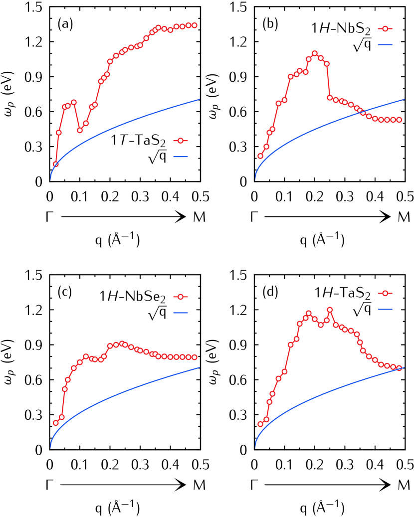
The plasmon dispersion of monolayer TMDs has been studied extensively in recent years [54, 30, 31, 55]. While the dispersion of plasmons in three-dimensional bulk systems commences with finite energy at a wavevector of , conventional plasmons in 2D metallic systems follow a relationship. To ascertain plasmon excitations, we identify the peaks in the loss function , wherein represents the macroscopic dielectric function. Fig. 12 displays the calculated plasmon dispersion for the monolayers of four compounds: 1-TaS2, 1-NbS2, 1-NbSe2, and 1-TaS2 and compared with the plasmon dispersion. Surprisingly, materials of the form MX2 (M=Nb, Ta) deviate from the anticipated plasmon dispersion observed in conventional 2D metallic systems. Particularly striking is the nearly linear dispersion of plasmons in the monolayer metallic 1-NbS2 at small , which transitions to a nearly dispersionless behavior within an intermediate range of wavevectors ( Å-1 to 0.3 Å-1). Moreover, we observe a negative slope in the dispersion relation for 1-MX2 at larger . This deviation from the behavior is most pronounced in the 1 structure due to its comparatively greater long-range interaction compared to the 1 structure. Notably, these findings align well with electron energy loss spectroscopy (EELS) measurements conducted by other researchers, who noted a negative slope in the plasmon dispersion of 1-TaS2, 1-TaSe2, and 1-NbSe2 [56]. The negative plasmon dispersion in TMDs has been attributed to the strong electron-electron interactions in these materials. These interactions can lead to the formation of collective charge fluctuations, which can couple to the plasmons and modify their dispersion. The results of our study provide new insights into the plasmon properties of TMDs. These insights could be used to design TMD-based plasmonic devices with novel functionalities.
III.4 Frequency dependency of screened Coulomb interaction
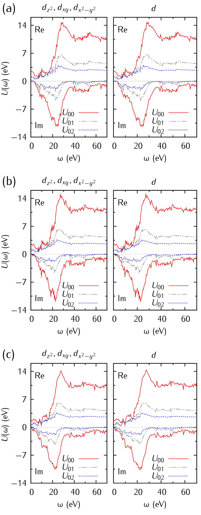
In this section, we investigate the frequency-dependent behavior of the partially . We focus on the semiconducting 1-MoS2, metallic 1-NbS2, and metallic 1-NbS2 compounds. We analyze these materials with respect to two distinct correlated subspaces. The real and imaginary components of the computed on-site interaction , as well as the interactions of the first and second nearest neighbors, namely and , are shown in Fig. 13 for these materials. Given the structural and compositional similarities among them, the frequency-dependent behaviors of the screened Coulomb interactions exhibit comparable trends across all three systems.
In the case of 1-MoS2, the profile displays smooth behavior with minor fluctuations up to a frequency of 15 eV. Beyond this point, it experiences linear growth, ultimately peaking at the plasmon frequency of approximately 25 eV (which is also evident as a peak in the imaginary part of ). Subsequently, as the frequency increases further, it asymptotically approaches the static value of 9.5 eV characteristic of 1-MoS2.
For 1-NbS2 and 1-NbS2, both metallic systems, the Coulomb interactions exhibit more pronounced variations at lower frequencies. These strong variations can be attributed to the narrow bands around the Fermi level in these materials. Notably, the frequency dependency of shows similar trends to the and cases. The decline in at lower frequencies, around 5 eV, in metallic systems arises from effective screening influenced by states around the Fermi level, which forms a bandwidth of approximately 5 eV. This behavior extends to the off-site Coulomb interactions (nearest-neighbor and next nearest-neighbor ), as shown by the dashed lines. One can imagine that the variations in the effective Coulomb interaction at low frequencies will average out, so that the static limit may still be appropriate for model Hamiltonian studies.
IV Conclusions
In this work, we have employed the random phase approximation within the FLAPW method to study the on-site and -dependent screening of the Coulomb interactions (partially screened) and (fully screened) in 2D TMDs MX2 (M=Mo, W, Nb, Ta; X = S, Se, Te). Our results show that the -dependent screening in semiconducting compounds like MoS2 deviates substantially from the conventional behavior, i.e., and cannot be expressed by a simple static dielectric constant . We found that the short-range interactions are strongly screened, while the long-range interactions are weakly screened, i.e., they decay much slower than the bare interaction. This nonconventional screening of the Coulomb interaction in 2D TMDs can be attributed to the reduced dimensionality of these materials. This -dependent nonconventional screening explains the large exciton binding energies and deviations from the usual hydrogenic Rydberg series of energy levels of the excitonic states in semiconducting monolayer TMDs.
Our results also show that metallic TMDs like NbS2 in the structure exhibit a correlation strength , which is significantly larger than the corresponding values in elementary TMs. This is due to the strong -dependent screening, which leads to a larger effective Coulomb interaction. The large ratio suggests that these materials are prone to Mott insulating behavior, which has been experimentally observed in the reconstructed lattice. Using the calculated parameters for undistorted structure, we extract the on-site effective and nearest neighbor Coulomb interaction parameters for reconstructed CCDW NbX2 and TaX2 compounds. Strictly speaking, for the reconstructed star of David -MX2 (M=Nb, Ta) structure, the large eV estimated for electrons compared with the relatively small bandwidth 0.02 eV satisfies the condition of . Furthermore, we found that the long-range Coulomb interactions remain sizable in metallic TMDs, despite the metallic nature of these materials. This is due to the reduced screening at long distances. The long-range Coulomb interactions can lead to the existence of intriguing plasmons in the monolayer of TMDs and the appearance of CDW order.
This study presents a comprehensive understanding of the Coulomb interactions in both semiconducting and metallic 2D TMDs. Furthermore, the derived Coulomb interaction parameters can be effectively employed in model Hamiltonians and DFT+ (DFT++) methods, consequently boosting the predictive power of these techniques.
Acknowledgements.
E.Ş and I.M. acknowledge support from Sonderforschungsbereich TRR 227 of Deutsche Forschungsgemeinschaft (DFG) and funding provided by the European Union (EFRE), Grant No: ZS/2016/06/79307.References
- Geim [2021] A. K. Geim, Exploring two-dimensional empty space, Nano Letters 21, 6356 (2021).
- Li and Wong [2017] Z. Li and S. L. Wong, Functionalization of 2d transition metal dichalcogenides for biomedical applications, Materials Science and Engineering: C 70, 1095 (2017).
- Chen et al. [2022a] H. Chen, J. Zhang, D. Kan, J. He, M. Song, J. Pang, S. Wei, and K. Chen, The recent progress of two-dimensional transition metal dichalcogenides and their phase transition, Crystals 12, 1381 (2022a).
- Yang et al. [2023] F. Yang, P. Hu, F. F. Yang, B. Chen, F. Yin, R. Sun, K. Hao, F. Zhu, K. Wang, and Z. Yin, Emerging enhancement and regulation strategies for ferromagnetic 2D transition metal dichalcogenides, Advanced Science , 2300952 (2023).
- Hossain et al. [2022] M. Hossain, B. Qin, B. Li, and X. Duan, Synthesis, characterization, properties and applications of two-dimensional magnetic materials, Nano Today 42, 101338 (2022).
- Kumbhakar et al. [2021] P. Kumbhakar, C. Chowde Gowda, and C. S. Tiwary, Advance optical properties and emerging applications of 2d materials, Frontiers in Materials 8, 721514 (2021).
- Gong et al. [2017] C. Gong, Y. Zhang, W. Chen, J. Chu, T. Lei, J. Pu, L. Dai, C. Wu, Y. Cheng, T. Zhai, et al., Electronic and optoelectronic applications based on 2D novel anisotropic transition metal dichalcogenides, Advanced Science 4, 1700231 (2017).
- Mueller and Malic [2018] T. Mueller and E. Malic, Exciton physics and device application of two-dimensional transition metal dichalcogenide semiconductors, npj 2D Materials and Applications 2, 29 (2018).
- Norden et al. [2019] T. Norden, C. Zhao, P. Zhang, R. Sabirianov, A. Petrou, and H. Zeng, Giant valley splitting in monolayer ws2 by magnetic proximity effect, Nature communications 10, 4163 (2019).
- Zhao et al. [2021] S. Zhao, X. Li, B. Dong, H. Wang, H. Wang, Y. Zhang, Z. Han, and H. Zhang, Valley manipulation in monolayer transition metal dichalcogenides and their hybrid systems: status and challenges, Reports on Progress in Physics 84, 026401 (2021).
- Edwards et al. [2023] B. Edwards, O. Dowinton, A. Hall, P. Murgatroyd, S. Buchberger, T. Antonelli, G.-R. Siemann, A. Rajan, E. A. Morales, A. Zivanovic, et al., Giant valley-zeeman coupling in the surface layer of an intercalated transition metal dichalcogenide, Nature Materials 22, 459 (2023).
- Du et al. [2019] L. Du, J. Tang, J. Liang, M. Liao, Z. Jia, Q. Zhang, Y. Zhao, R. Yang, D. Shi, L. Gu, et al., Giant valley coherence at room temperature in 3r ws2 with broken inversion symmetry, Research 10.34133/2019/6494565 (2019).
- Ramasubramaniam et al. [2011] A. Ramasubramaniam, D. Naveh, and E. Towe, Tunable band gaps in bilayer transition-metal dichalcogenides, Physical Review B 84, 10.1103/physrevb.84.205325 (2011).
- Sun et al. [2023] X. Sun, Y. Chen, D. Zhao, T. Taniguchi, K. Watanabe, J. Wang, and J. Xue, Measuring band modulation of MoS2 with ferroelectric gates, Nano Letters 23, 2114 (2023).
- Lembke et al. [2015] D. Lembke, S. Bertolazzi, and A. Kis, Single-layer MoS2 electronics, Accounts of Chemical Research 48, 100 (2015).
- Radisavljevic et al. [2011] B. Radisavljevic, M. B. Whitwick, and A. Kis, Integrated circuits and logic operations based on single-layer MoS2, ACS Nano 5, 9934 (2011).
- Liu et al. [2015] X. Liu, T. Galfsky, Z. Sun, F. Xia, E.-c. Lin, Y.-H. Lee, S. Kéna-Cohen, and V. M. Menon, Strong light-matter coupling in two-dimensional atomic crystals, Nature Photonics 9, 30 (2015).
- Shafi et al. [2022] A. M. Shafi, F. Ahmed, H. A. Fernandez, M. G. Uddin, X. Cui, S. Das, Y. Dai, V. Khayrudinov, H. H. Yoon, L. Du, et al., Inducing strong light-matter coupling and optical anisotropy in monolayer MoS2 with high refractive index nanowire, ACS applied materials & interfaces 14, 31140 (2022).
- Zeng and Liu [2018] Q. Zeng and Z. Liu, Novel optoelectronic devices: Transition-metal-dichalcogenide-based 2D heterostructures, Advanced Electronic Materials 4, 1700335 (2018).
- Balendhran et al. [2013] S. Balendhran, S. Walia, H. Nili, J. Z. Ou, S. Zhuiykov, R. B. Kaner, S. Sriram, M. Bhaskaran, and K. Kalantar-zadeh, Two-dimensional molybdenum trioxide and dichalcogenides, Advanced Functional Materials 23, 3952 (2013).
- Zhang and Zhang [2017] G. Zhang and Y.-W. Zhang, Thermoelectric properties of two-dimensional transition metal dichalcogenides, Journal of Materials Chemistry C 5, 7684 (2017).
- Kanahashi et al. [2020] K. Kanahashi, J. Pu, and T. Takenobu, 2d materials for large-area flexible thermoelectric devices, Advanced Energy Materials 10, 1902842 (2020).
- Jia et al. [2022] P.-Z. Jia, J.-P. Xie, X.-K. Chen, Y. Zhang, X. Yu, Y.-J. Zeng, Z.-X. Xie, Y.-X. Deng, and W.-X. Zhou, Recent progress of two-dimensional heterostructures for thermoelectric applications, Journal of Physics: Condensed Matter 35, 073001 (2022).
- Şaşıoğlu and Mertig [2023] E. Şaşıoğlu and I. Mertig, Theoretical prediction of semiconductor-free negative differential resistance tunnel diodes with high peak-to-valley current ratios based on two-dimensional cold metals, ACS Applied Nano Materials 6, 3758 (2023).
- Qiu et al. [2018] C. Qiu, F. Liu, L. Xu, B. Deng, M. Xiao, J. Si, L. Lin, Z. Zhang, J. Wang, H. Guo, H. Peng, and L.-M. Peng, Dirac-source field-effect transistors as energy-efficient, high-performance electronic switches, Science 361, 387 (2018).
- Liu [2020] F. Liu, Switching at less than 60 mv/decade with a “cold” metal as the injection source, Phys. Rev. Appl. 13, 064037 (2020).
- Marin et al. [2020] E. G. Marin, D. Marian, M. Perucchini, G. Fiori, and G. Iannaccone, Lateral heterostructure field-effect transistors based on two-dimensional material stacks with varying thickness and energy filtering source, ACS Nano 14, 1982 (2020).
- Logoteta et al. [2020] D. Logoteta, J. Cao, M. Pala, P. Dollfus, Y. Lee, and G. Iannaccone, Cold-source paradigm for steep-slope transistors based on van der waals heterojunctions, Phys. rev. res. 2, 043286 (2020).
- Tang et al. [2021] Z. Tang, C. Liu, X. Huang, S. Zeng, L. Liu, J. Li, Y.-G. Jiang, D. W. Zhang, and P. Zhou, A steep-slope MoS2/graphene dirac-source field-effect transistor with a large drive current, Nano Lett. 21, 1758 (2021).
- Cudazzo et al. [2016] P. Cudazzo, E. Müller, C. Habenicht, M. Gatti, H. Berger, M. Knupfer, A. Rubio, and S. Huotari, Negative plasmon dispersion in 2H-NbS2 beyond the charge-density-wave interpretation, New Journal of Physics 18, 103050 (2016).
- da Jornada et al. [2020a] F. H. da Jornada, L. Xian, A. Rubio, and S. G. Louie, Universal slow plasmons and giant field enhancement in atomically thin quasi-two-dimensional metals, Nature communications 11, 1013 (2020a).
- Ritschel et al. [2015] T. Ritschel, J. Trinckauf, K. Koepernik, B. Büchner, M. v. Zimmermann, H. Berger, Y. I. Joe, P. Abbamonte, and J. Geck, Orbital textures and charge density waves in transition metal dichalcogenides, Nature Physics 11, 328 (2015).
- Chen et al. [2020a] Y. Chen, W. Ruan, M. Wu, S. Tang, H. Ryu, H.-Z. Tsai, R. L. Lee, S. Kahn, F. Liou, C. Jia, et al., Strong correlations and orbital texture in single-layer 1T-TaSe2, Nature Physics 16, 218 (2020a).
- Lee et al. [2021] M. Lee, M. Šiškins, S. Mañas-Valero, E. Coronado, P. G. Steeneken, and H. S. J. van der Zant, Study of charge density waves in suspended 2H-TaS2 and 2H-TaSe2 by nanomechanical resonance, Applied Physics Letters 118, 193105 (2021).
- Sipos et al. [2008] B. Sipos, A. F. Kusmartseva, A. Akrap, H. Berger, L. Forró, and E. Tutiš, From mott state to superconductivity in 1T-TaS2, Nature Materials 7, 960 (2008).
- Navarro-Moratalla et al. [2016] E. Navarro-Moratalla, J. O. Island, S. Manas-Valero, E. Pinilla-Cienfuegos, A. Castellanos-Gomez, J. Quereda, G. Rubio-Bollinger, L. Chirolli, J. A. Silva-Guillén, N. Agraït, et al., Enhanced superconductivity in atomically thin TaS2, Nature Communications 7, 11043 (2016).
- Xu et al. [2014] Y. Xu, X. Liu, and W. Guo, Tensile strain induced switching of magnetic states in NbSe2 and NbS2 single layers, Nanoscale 6, 12929 (2014).
- Güller et al. [2016] F. Güller, V. L. Vildosola, and A. M. Llois, Spin density wave instabilities in the NbSe2 monolayer, Physical Review B 93, 10.1103/physrevb.93.094434 (2016).
- Pasquier and Yazyev [2022] D. Pasquier and O. V. Yazyev, Ab initio theory of magnetism in two-dimensional 1T-TaS2, Physical Review B 105, 10.1103/physrevb.105.l081106 (2022).
- Chen et al. [2022b] H. Chen, J. Zhang, D. Kan, J. He, M. Song, J. Pang, S. Wei, and K. Chen, The recent progress of two-dimensional transition metal dichalcogenides and their phase transition, Crystals 12, 1381 (2022b).
- Maghool et al. [2023] S. Maghool, H. Hadipour, and H. Rahimpour, Magnetism in single-layer of ZrSe2 by substituting 3d transition metals for zr: Structural symmetry versus exchange splitting, Computational Materials Science 216, 111823 (2023).
- Aghaee et al. [2022] A. K. Aghaee, S. Belbasi, and H. Hadipour, Ab initio calculation of the effective coulomb interactions in MX2 (M=Ti, V, Cr, Mn, Fe, Co, Ni; X=S, Se, Te): Intrinsic magnetic ordering and mott phase, Physical Review B 105, 10.1103/physrevb.105.115115 (2022).
- Yekta et al. [2021] Y. Yekta, H. Hadipour, E. Şaşıoğlu, C. Friedrich, S. Jafari, S. Blügel, and I. Mertig, Strength of effective coulomb interaction in two-dimensional transition-metal halides MX2 and MX3 (M= Ti, V, Cr, Mn, Fe, Co, Ni; X= Cl, Br, I), Physical Review Materials 5, 034001 (2021).
- Ramasubramaniam [2012a] A. Ramasubramaniam, Large excitonic effects in monolayers of molybdenum and tungsten dichalcogenides, Physical Review B 86, 115409 (2012a).
- Qiu et al. [2013a] D. Y. Qiu, F. H. Da Jornada, and S. G. Louie, Optical spectrum of MoS2: many-body effects and diversity of exciton states, Physical review letters 111, 216805 (2013a).
- Chernikov et al. [2014a] A. Chernikov, T. C. Berkelbach, H. M. Hill, A. Rigosi, Y. Li, B. Aslan, D. R. Reichman, M. S. Hybertsen, and T. F. Heinz, Exciton binding energy and non-hydrogenic rydberg series in monolayer WS2, Physical review letters 113, 076802 (2014a).
- He et al. [2014] K. He, N. Kumar, L. Zhao, Z. Wang, K. F. Mak, H. Zhao, and J. Shan, Tightly bound excitons in monolayer WSe2, Physical review letters 113, 026803 (2014).
- Ugeda et al. [2014] M. M. Ugeda, A. J. Bradley, S.-F. Shi, F. H. Da Jornada, Y. Zhang, D. Y. Qiu, W. Ruan, S.-K. Mo, Z. Hussain, Z.-X. Shen, et al., Giant bandgap renormalization and excitonic effects in a monolayer transition metal dichalcogenide semiconductor, Nature materials 13, 1091 (2014).
- Kobayashi et al. [2023] Y. Kobayashi, C. Heide, A. C. Johnson, V. Tiwari, F. Liu, D. A. Reis, T. F. Heinz, and S. Ghimire, Floquet engineering of strongly driven excitons in monolayer tungsten disulfide, Nature Physics 10.1038/s41567-022-01849-9 (2023).
- Chen et al. [2023] Y. Chen, H. Liang, L. Loh, Y. Ho, I. Verzhbitskiy, K. Watanabe, T. Taniguchi, M. Bosman, A. A. Bettiol, and G. Eda, Gate-tunable bound exciton manifolds in monolayer MoSe2, Nano Letters 23, 4456 (2023).
- Chernikov et al. [2014b] A. Chernikov, T. C. Berkelbach, H. M. Hill, A. Rigosi, Y. Li, B. Aslan, D. R. Reichman, M. S. Hybertsen, and T. F. Heinz, Exciton binding energy and nonhydrogenic rydberg series in monolayer WS2, Physical Review Letters 113, 10.1103/physrevlett.113.076802 (2014b).
- Qiu et al. [2013b] D. Y. Qiu, F. H. da Jornada, and S. G. Louie, Optical spectrum of MoS2: Many-body effects and diversity of exciton states, Physical Review Letters 111, 10.1103/physrevlett.111.216805 (2013b).
- Liu et al. [2021a] L. Liu, H. Yang, Y. Huang, X. Song, Q. Zhang, Z. Huang, Y. Hou, Y. Chen, Z. Xu, T. Zhang, X. Wu, J. Sun, Y. Huang, F. Zheng, X. Li, Y. Yao, H.-J. Gao, and Y. Wang, Direct identification of mott hubbard band pattern beyond charge density wave superlattice in monolayer 1T-NbSe2, Nature Communications 12, 10.1038/s41467-021-22233-w (2021a).
- Song et al. [2021] C. Song, X. Yuan, C. Huang, S. Huang, Q. Xing, C. Wang, C. Zhang, Y. Xie, Y. Lei, F. Wang, L. Mu, J. Zhang, F. Xiu, and H. Yan, Plasmons in the van der waals charge-density-wave material 2H-TaSe2, Nature Communications 12, 10.1038/s41467-020-20720-0 (2021).
- da Jornada et al. [2020b] F. H. da Jornada, L. Xian, A. Rubio, and S. G. Louie, Universal slow plasmons and giant field enhancement in atomically thin quasi-two-dimensional metals, Nature Communications 11, 10.1038/s41467-020-14826-8 (2020b).
- van Wezel et al. [2011] J. van Wezel, R. Schuster, A. König, M. Knupfer, J. van den Brink, H. Berger, and B. Büchner, Effect of charge order on the plasmon dispersion in transition-metal dichalcogenides, Physical Review Letters 107, 10.1103/physrevlett.107.176404 (2011).
- Chen et al. [2018] P. Chen, W. W. Pai, Y.-H. Chan, W.-L. Sun, C.-Z. Xu, D.-S. Lin, M. Y. Chou, A.-V. Fedorov, and T.-C. Chiang, Large quantum-spin-hall gap in single-layer 1T’-WSe2, Nature Communications 9, 10.1038/s41467-018-04395-2 (2018).
- Ugeda et al. [2018] M. M. Ugeda, A. Pulkin, S. Tang, H. Ryu, Q. Wu, Y. Zhang, D. Wong, Z. Pedramrazi, A. Martín-Recio, Y. Chen, F. Wang, Z.-X. Shen, S.-K. Mo, O. V. Yazyev, and M. F. Crommie, Observation of topologically protected states at crystalline phase boundaries in single-layer WSe2, Nature Communications 9, 10.1038/s41467-018-05672-w (2018).
- Wehling et al. [2011] T. O. Wehling, E. Şaşıoğlu, C. Friedrich, A. I. Lichtenstein, M. I. Katsnelson, and S. Blügel, Strength of effective coulomb interactions in graphene and graphite, Physical Review Letters 106, 10.1103/physrevlett.106.236805 (2011).
- Hwang and Sarma [2007] E. H. Hwang and S. D. Sarma, Dielectric function, screening, and plasmons in two-dimensional graphene, Physical Review B 75, 10.1103/physrevb.75.205418 (2007).
- Hadipour et al. [2018] H. Hadipour, E. Şaşıoğlu, F. Bagherpour, C. Friedrich, S. Blügel, and I. Mertig, Screening of long-range coulomb interaction in graphene nanoribbons: Armchair versus zigzag edges, Physical Review B 98, 10.1103/physrevb.98.205123 (2018).
- Şaşıoğlu et al. [2017] E. Şaşıoğlu, H. Hadipour, C. Friedrich, S. Blügel, and I. Mertig, Strength of effective coulomb interactions and origin of ferromagnetism in hydrogenated graphene, Physical Review B 95, 10.1103/physrevb.95.060408 (2017).
- Şaşıoğlu et al. [2011] E. Şaşıoğlu, C. Friedrich, and S. Blügel, Effective coulomb interaction in transition metals from constrained random-phase approximation, Physical Review B 83, 121101 (2011).
- Hadipour and Yekta [2019] H. Hadipour and Y. Yekta, Ab initio study of the effective coulomb interactions and stoner ferromagnetism in M2C and M2CO2 MX-enes (M=Sc,Ti,V,Cr,Fe,Zr,Nb,Mo,Hf,Ta), Physical Review B 100, 10.1103/physrevb.100.195118 (2019).
- Kim et al. [2023] T. J. Kim, M. Y. Jeong, and M. J. Han, First principles investigation of screened coulomb interaction and electronic structure of low-temperature phase TaS2, iScience 26, 106681 (2023).
- Darancet et al. [2014] P. Darancet, A. J. Millis, and C. A. Marianetti, Three-dimensional metallic and two-dimensional insulating behavior in octahedral tantalum dichalcogenides, Physical Review B 90, 10.1103/physrevb.90.045134 (2014).
- van Loon et al. [2018] E. G. van Loon, M. Rösner, G. Schönhoff, M. I. Katsnelson, and T. O. Wehling, Competing coulomb and electron-phonon interactions in NbS2, npj Quantum Materials 3, 32 (2018).
- Haastrup et al. [2018] S. Haastrup, M. Strange, M. Pandey, T. Deilmann, P. S. Schmidt, N. F. Hinsche, M. N. Gjerding, D. Torelli, P. M. Larsen, A. C. Riis-Jensen, J. Gath, K. W. Jacobsen, J. J. Mortensen, T. Olsen, and K. S. Thygesen, The computational 2d materials database: high-throughput modeling and discovery of atomically thin crystals, 2d Mater. 5, 042002 (2018).
- Manzeli et al. [2017] S. Manzeli, D. Ovchinnikov, D. Pasquier, O. V. Yazyev, and A. Kis, 2D transition metal dichalcogenides, Nature Reviews Materials 2, 17033 (2017).
- Wang et al. [2018] J. Wang, Y. Wei, H. Li, X. Huang, and H. Zhang, Crystal phase control in two-dimensional materials, Science China Chemistry 61, 1227 (2018).
- Qian et al. [2020] Z. Qian, L. Jiao, and L. Xie, Phase engineering of two-dimensional transition metal dichalcogenides, Chinese Journal of Chemistry 38, 753 (2020).
- Chen et al. [2020b] K. Chen, J. Deng, Q. Shi, X. Ding, J. Sun, S. Yang, and J. Z. Liu, Charge doping induced reversible multistep structural phase transitions and electromechanical actuation in two-dimensional 1T’-MoS2, Nanoscale 12, 12541 (2020b).
- Voiry et al. [2015] D. Voiry, A. Mohite, and M. Chhowalla, Phase engineering of transition metal dichalcogenides, Chemical Society Reviews 44, 2702 (2015).
- Choe et al. [2016] D.-H. Choe, H.-J. Sung, and K. J. Chang, Understanding topological phase transition in monolayer transition metal dichalcogenides, Physical Review B 93, 125109 (2016).
- Zhao et al. [2018] W. Zhao, J. Pan, Y. Fang, X. Che, D. Wang, K. Bu, and F. Huang, Metastable MoS2: crystal structure, electronic band structure, synthetic approach and intriguing physical properties, Chemistry–A European Journal 24, 15942 (2018).
- [76] The FLEUR project, https://www.flapw.de/.
- Perdew et al. [1996] J. P. Perdew, K. Burke, and M. Ernzerhof, Generalized gradient approximation made simple, Physical review letters 77, 3865 (1996).
- Pizzi et al. [2020] G. Pizzi, V. Vitale, R. Arita, S. Blügel, F. Freimuth, G. Géranton, M. Gibertini, D. Gresch, C. Johnson, T. Koretsune, et al., Wannier90 as a community code: new features and applications, Journal of Physics: Condensed Matter 32, 165902 (2020).
- Marzari and Vanderbilt [1997] N. Marzari and D. Vanderbilt, Maximally localized generalized wannier functions for composite energy bands, Physical review B 56, 12847 (1997).
- Mostofi et al. [2008] A. A. Mostofi, J. R. Yates, Y.-S. Lee, I. Souza, D. Vanderbilt, and N. Marzari, wannier90: A tool for obtaining maximally-localized wannier functions, Computer physics communications 178, 685 (2008).
- Freimuth et al. [2008] F. Freimuth, Y. Mokrousov, D. Wortmann, S. Heinze, and S. Blügel, Maximally localized wannier functions within the flapw formalism, Physical Review B 78, 035120 (2008).
- Aryasetiawan et al. [2004] F. Aryasetiawan, M. Imada, A. Georges, G. Kotliar, S. Biermann, and A. Lichtenstein, Frequency-dependent local interactions and low-energy effective models from electronic structure calculations, Physical Review B 70, 195104 (2004).
- Aryasetiawan et al. [2006] F. Aryasetiawan, K. Karlsson, O. Jepsen, and U. Schönberger, Calculations of hubbard u from first-principles, Physical Review B 74, 125106 (2006).
- Miyake et al. [2009] T. Miyake, F. Aryasetiawan, and M. Imada, Ab initio procedure for constructing effective models of correlated materials with entangled band structure, Physical Review B 80, 155134 (2009).
- Nomura et al. [2012] Y. Nomura, M. Kaltak, K. Nakamura, C. Taranto, S. Sakai, A. Toschi, R. Arita, K. Held, G. Kresse, and M. Imada, Effective on-site interaction for dynamical mean-field theory, Physical Review B 86, 085117 (2012).
- Shih et al. [2012] B.-C. Shih, Y. Zhang, W. Zhang, and P. Zhang, Screened coulomb interaction of localized electrons in solids from first principles, Physical Review B 85, 045132 (2012).
- Schindlmayr et al. [2010] A. Schindlmayr, C. Friedrich, E. Sasioglu, and S. Blügel, First-principles calculation of electronic excitations in solids with spex, Zeitschrift für Physikalische Chemie 224, 357 (2010).
- Friedrich et al. [2010] C. Friedrich, S. Blügel, and A. Schindlmayr, Efficient implementation of the gw approximation within the all-electron FLAPW method, Physical Review B 81, 125102 (2010).
- Anisimov et al. [1993] V. I. Anisimov, I. Solovyev, M. Korotin, M. Czyżyk, and G. Sawatzky, Density-functional theory and NiO photoemission spectra, Physical Review B 48, 16929 (1993).
- Anisimov et al. [2010] V. Anisimov, Y. Izyumov, V. Anisimov, and Y. Izyumov, Electronic structure calculations in one-electron approximation, Electronic Structure of Strongly Correlated Materials , 9 (2010).
- Şaşıoğlu et al. [2012] E. Şaşıoğlu, C. Friedrich, and S. Blügel, Strength of the effective coulomb interaction at metal and insulator surfaces, Physical review letters 109, 146401 (2012).
- Kamil et al. [2018] E. Kamil, J. Berges, G. Schönhoff, M. Rösner, M. Schüler, G. Sangiovanni, and T. O. Wehling, Electronic structure of single layer 1T-NbSe2: interplay of lattice distortions, non-local exchange, and mott-hubbard correlations, Journal of Physics: Condensed Matter 30, 325601 (2018).
- Andersen et al. [2015] K. Andersen, S. Latini, and K. S. Thygesen, Dielectric genome of van der waals heterostructures, Nano Letters 15, 4616–4621 (2015).
- Trolle et al. [2017] M. L. Trolle, T. G. Pedersen, and V. Véniard, Model dielectric function for 2d semiconductors including substrate screening, Scientific Reports 7, 39844 (2017).
- Hüser et al. [2013] F. Hüser, T. Olsen, and K. S. Thygesen, How dielectric screening in two-dimensional crystals affects the convergence of excited-state calculations: Monolayer mos2, Physical Review B 88, 245309 (2013).
- Nazarov et al. [2014] V. U. Nazarov, F. Alharbi, T. S. Fisher, and S. Kais, Time-dependent density functional theory of coupled electronic lattice motion in quasi-two-dimensional crystals, Phys. Rev. B 89, 195423 (2014).
- Rost et al. [2023] S. Rost, S. Blügel, and C. Friedrich, Efficient calculation of -integrated electron energy loss spectra: Application to monolayers of and graphene, Phys. Rev. B 107, 085132 (2023).
- Molina-Sánchez and Wirtz [2011] A. Molina-Sánchez and L. Wirtz, Phonons in single-layer and few-layer mos2, Physical Review B 84, 155413 (2011).
- Ramasubramaniam [2012b] A. Ramasubramaniam, Large excitonic effects in monolayers of molybdenum and tungsten dichalcogenides, Physical Review B 86, 115409 (2012b).
- Cheiwchanchamnangij and Lambrecht [2012] T. Cheiwchanchamnangij and W. R. L. Lambrecht, Quasiparticle band structure calculation of monolayer, bilayer, and bulk mos2, Physical Review B 85, 205302 (2012).
- Keum et al. [2015] D. H. Keum, S. Cho, J. H. Kim, D.-H. Choe, H.-J. Sung, M. Kan, H. Kang, J.-Y. Hwang, S. W. Kim, H. Yang, et al., Bandgap opening in few-layered monoclinic MoTe2, Nature Physics 11, 482 (2015).
- Huang et al. [2016] H. Huang, X. Fan, D. J. Singh, H. Chen, Q. Jiang, and W. Zheng, Controlling phase transition for single-layer MTe2 (M= Mo and W): modulation of the potential barrier under strain, Physical Chemistry Chemical Physics 18, 4086 (2016).
- Park et al. [2020] J. C. Park, E. Jung, S. Lee, J. Hwang, and Y. H. Lee, Evidence of shallow band gap in ultrathin 1T’-MoTe2 via infrared spectroscopy, Physical Review B 101, 235434 (2020).
- Song et al. [2018] P. Song, C. Hsu, M. Zhao, X. Zhao, T.-R. Chang, J. Teng, H. Lin, and K. P. Loh, Few-layer 1T’-MoTe2 as gapless semimetal with thickness dependent carrier transport, 2D Materials 5, 031010 (2018).
- Chen et al. [2015] X. Chen, Z. Wu, S. Xu, L. Wang, R. Huang, Y. Han, W. Ye, W. Xiong, T. Han, G. Long, et al., Probing the electron states and metal-insulator transition mechanisms in molybdenum disulphide vertical heterostructures, Nature communications 6, 6088 (2015).
- Kotov et al. [2012] V. N. Kotov, B. Uchoa, V. M. Pereira, F. Guinea, and A. H. C. Neto, Electron-electron interactions in graphene: Current status and perspectives, Reviews of Modern Physics 84, 1067 (2012).
- Neroni et al. [2019] A. Neroni, E. Şaşıoğlu, H. Hadipour, C. Friedrich, S. Blügel, I. Mertig, and M. Ležaić, First-principles calculation of the effective on-site coulomb interaction parameters for Sr2ABO6 (A=Cr, Mn, Fe, Co, Ni, and B=Mo, W) double perovskites, Physical Review B 100, 10.1103/physrevb.100.115113 (2019).
- Lin et al. [2019] H. Lin, W. Huang, K. Zhao, S. Qiao, Z. Liu, J. Wu, X. Chen, and S.-H. Ji, Scanning tunneling spectroscopic study of monolayer 1T-TaS2 and 1T-TaSe2, Nano Research 13, 133 (2019).
- Hadipour [2019] H. Hadipour, Screening of coulomb interaction and pi magnetism in defected graphene, Physical Review B 99, 10.1103/physrevb.99.075102 (2019).
- Huang et al. [2017] B. Huang, G. Clark, E. Navarro-Moratalla, D. R. Klein, R. Cheng, K. L. Seyler, D. Zhong, E. Schmidgall, M. A. McGuire, D. H. Cobden, et al., Layer-dependent ferromagnetism in a van der waals crystal down to the monolayer limit, Nature 546, 270 (2017).
- Seyler et al. [2017] K. L. Seyler, D. Zhong, D. R. Klein, S. Gao, X. Zhang, B. Huang, E. Navarro-Moratalla, L. Yang, D. H. Cobden, M. A. McGuire, W. Yao, D. Xiao, P. Jarillo-Herrero, and X. Xu, Ligand-field helical luminescence in a 2D ferromagnetic insulator, Nature Physics 14, 277 (2017).
- Tian et al. [2019] S. Tian, J.-F. Zhang, C. Li, T. Ying, S. Li, X. Zhang, K. Liu, and H. Lei, Ferromagnetic van der waals crystal VI3, Journal of the American Chemical Society 141, 5326 (2019).
- Wang et al. [2021] X. Wang, D. Li, Z. Li, C. Wu, C.-M. Che, G. Chen, and X. Cui, Ferromagnetism in 2D vanadium diselenide, ACS Nano 15, 16236 (2021).
- Kim et al. [2018] S. Y. Kim, T. Y. Kim, L. J. Sandilands, S. Sinn, M.-C. Lee, J. Son, S. Lee, K.-Y. Choi, W. Kim, B.-G. Park, C. Jeon, H.-D. Kim, C.-H. Park, J.-G. Park, S. Moon, and T. Noh, Charge-spin correlation in van der waals antiferromagnet NiPS3, Physical Review Letters 120, 10.1103/physrevlett.120.136402 (2018).
- Butler et al. [2020] C. J. Butler, M. Yoshida, T. Hanaguri, and Y. Iwasa, Mottness versus unit-cell doubling as the driver of the insulating state in 1T-TaS2, Nature Communications 11, 10.1038/s41467-020-16132-9 (2020).
- Wang et al. [2017] H. Wang, X. Huang, J. Lin, J. Cui, Y. Chen, C. Zhu, F. Liu, Q. Zeng, J. Zhou, P. Yu, et al., High-quality monolayer superconductor nbse2 grown by chemical vapour deposition, Nature communications 8, 394 (2017).
- Nakata et al. [2021] Y. Nakata, K. Sugawara, A. Chainani, H. Oka, C. Bao, S. Zhou, P.-Y. Chuang, C.-M. Cheng, T. Kawakami, Y. Saruta, et al., Robust charge-density wave strengthened by electron correlations in monolayer 1T-TaSe2 and 1T-NbSe2, Nature communications 12, 5873 (2021).
- Wang et al. [2020] Y. Wang, W. Yao, Z. Xin, T. Han, Z. Wang, L. Chen, C. Cai, Y. Li, and Y. Zhang, Band insulator to mott insulator transition in 1T-TaS2, Nature communications 11, 4215 (2020).
- Petkov et al. [2022] V. Petkov, J. Peralta, B. Aoun, and Y. Ren, Atomic structure and mott nature of the insulating charge density wave phase of 1T-TaS2, Journal of Physics: Condensed Matter 34, 345401 (2022).
- Liu et al. [2021b] Z.-Y. Liu, S. Qiao, B. Huang, Q.-Y. Tang, Z.-H. Ling, W.-H. Zhang, H.-N. Xia, X. Liao, H. Shi, W.-H. Mao, et al., Charge transfer gap tuning via structural distortion in monolayer 1T-NbSe2, Nano Letters 21, 7005 (2021b).
- Kratochvilova et al. [2017] M. Kratochvilova, A. D. Hillier, A. R. Wildes, L. Wang, S.-W. Cheong, and J.-G. Park, The low-temperature highly correlated quantum phase in the charge-density-wave 1T-TaS2 compound, npj Quantum Materials 2, 42 (2017).
- Xi et al. [2015] X. Xi, L. Zhao, Z. Wang, H. Berger, L. Forró, J. Shan, and K. F. Mak, Strongly enhanced charge-density-wave order in monolayer NbSe2, Nature Nanotechnology 10, 765 (2015).