Amorphous Boron Nitride as a Diffusion Barrier to Cu Atoms
Abstract
This study focuses on amorphous boron nitride (-BN) as a novel diffusion barrier for advanced semiconductor technology, particularly addressing the critical challenge of copper diffusion in back-end-of-logic (BEOL) interconnects. Owing to its ultralow dielectric constant and robust barrier properties, -BN is examined as an alternative to conventional low-k dielectrics. The investigation primarily employs theoretical modeling, using a Gaussian Approximation Potential, to simulate and understand the atomic-level interactions and barrier mechanisms of -BN. This machine learning-based approach allows for realistic simulations of its amorphous structure, enabling the exploration of the impact of different film morphologies on barrier efficacy. Complementing the theoretical study, experimental analyses are conducted on Plasma-Enhanced Chemical Vapor Deposition (PECVD) grown -BN films, evaluating their effectiveness in preventing copper diffusion in silicon-based substrates. The results from both the theoretical and experimental investigations highlight the potential of -BN as a highly effective diffusion barrier, suitable for integration in nanoelectronics. This research not only proposes -BN as a promising candidate for BEOL interconnects but also demonstrates the synergy of advanced computational models and experimental methods in material innovation for semiconductor applications.
1 Introduction
Continuous down-scaling of devices and architectures has been the major goal of the electronic industry for decades to increase the performances and chip density, and reduce power consumption [1, 2, 3]. The technology of interconnects is also experiencing such extreme scale-down, with sustained efforts to improve the resistance of metals and to lower the dielectric constant of intermetal dielectrics (IMDs), for optimized control of signal delays such as RC delay. The diffusion barrier that prevents the interaction between metals and IMD is also becoming thinner and is required to have excellent blocking properties. Ultimately, the technology aims for an almost “barrier-free” structure. Two-dimensional (2D) materials, such as and have recently garnered attention as potential barrier materials. Indeed, recent studies have shown that , when synthesized through Atomic Layer Deposition (ALD), can act as an effective Cu diffusion barrier, potentially reducing barrier thickness down to 1-2 nm. Furthermore, the integration of dopants into such as Niobium (Nb) has been found to enhance its ability to block Cu atom diffusion, indicating its suitability for sub-5 nm technology nodes [4, 5]. However, while these 2D materials could act as efficient diffusion barriers, they also have a higher dielectric constant which would add to the RC-delay.
Hexagonal boron nitride () on the other hand could be a better choice given its low dielectric constant and higher bandgap. However, the practical application of these 2D materials is confronted with significant challenges. Integrating these materials into existing semiconductor manufacturing processes, especially developing a BEOL-compatible growth process for deposition on dielectrics remains a major challenge [6, 7, 8]. Moreover, the presence of defects in 2D materials, such as vacancy defects in hBN and , can lead to Cu accumulation, creating diffusion pathways that compromise the barrier’s effectiveness [9]. Amidst the ongoing quest for materials that can meet the stringent demands of advanced semiconductor technologies, amorphous boron nitride (-BN) emerges as a particularly compelling candidate. In contrast to h-BN, -BN does not suffer from dangling bonds and grain boundaries. In addition to its low temperature growth possibility, -BN films can be uniformly synthesized on various substrates (such as metals and dielectrics) with a controllable thickness. This makes -BN a desirable dielectric material and a diffusion barrier [10, 11]. Besides, -BN has been reported to have a low dielectric constant as a result of poor dipole alignment due to its amorphous nature [12]. While Hong et al.[2] reported an ultralow dielectric constant of 1.7 for 3 nm PECVD-grown -BN. Glavin et al.[11] pointed out that homonuclear bonds can open conductive pathways and increase the dielectric constant. They measured a device dielectric constant of atomic layer deposition (ALD)-grown -BN of 5.9 with a band gap of 4.5 eV [11]. Similarly, the dielectric constant of ALD grown -BN at 65 - 250 ºC is between 4.3 - 9.0 which increases with faster cooling. They observed that faster cooling leads to N deficiency and higher oxygen contamination, causing midgap states and higher dielectric constant [13]. Lin et al.[14] showed that the dielectric constant can be monitored during the growth process and used precursor, to ultimately achieve a dielectric constant of 2.1 for a sub-10 nm -BN film. Meanwhile, Abbas et al.[15] reported dielectric constant of 2.61 - 5.88 for sputtered -BN films with thicknesses ranging between 12 nm and 800 nm[15]. Due to its low dielectric constant, good mechanical properties, and thermal stability, -BN films have already been shown to act as efficient metal diffusion barriers. While Hong et al. [2] showed that 3 nm -BN film can stop Co diffusion at 600 ºC, Kim et al. [16] found that 7-nm--BN film can stop Cu diffusion up to 500 ℃. Hence, -BN seems to be the ideal dielectric material due to the ultralow dielectric constant and its great barrier properties. However, as shown in the literature [11, 14, 13, 17, 18], the properties and performance of -BN are determined by their morphology. Hence, ALD -BN with the correct composition could be an ideal dielectric material due to the potential low dielectric constant and excellent metal barrier properties.
An exhaustive experimental investigation of the morphology and properties of -BN would be quite time-consuming and expensive. On the other hand, atomistic simulations would allow us to study the materials at the atomic level and can provide insights into the relation between morphology and key parameters of materials faster with moderate computational cost. Notwithstanding, implementing an accurate modeling of highly disordered materials such as -BN is quite a challenging task. Due to the lack of long-range order, the simulation box of amorphous materials should be quite large. This becomes quickly prohibitive for ab initio calculations. On the other hand, simulations using classical MD with empirical potentials can deal with such large samples. However, due to simplifications and assumptions used to develop these interatomic potentials, classical MD cannot capture the diverse atomic environment of the amorphous material. These challenges can be overcome using machine learning-based approaches. Classical MD simulations with machine learning-based interatomic potential trained over ab initio calculations can deal with very large simulation boxes with an ab initio accuracy [19, 20].
Here, the relationship between the morphology of -BN structures and their barrier properties is assessed both theoretically and experimentally. First, we develop a Gaussian Approximation Potential (GAP) model to describe the interactions between -BN and Cu atoms. Later, we generate -BN films with different thicknesses, and by employing different parameters, we investigate their resulting morphologies and barrier properties. We also study the mechanical properties of generated -BN samples. Finally, we present an experimental investigation of the barrier performance of PECVD-grown 3-, 5- and 7-nm thick -BN films against Cu diffusion to the Si-based substrate and compare it with the simulations.
2 Methods
In this study, we utilize both experimental and theoretical methods to investigate how -BN can prevent copper diffusion. Initially, we train an interatomic potential model using the Gaussian Approximation Potential (GAP) framework. This model is then applied in molecular dynamics (MD) simulations to explore the relationship between the morphology, properties, and barrier performance of melt-quenched (MQ) -BN. These simulations consider variations in thickness and cooling rates. Subsequently, we measure the barrier properties of PECVD-grown -BN films of different thicknesses by detecting the presence of copper silicide crystals, which aids in correlating our experimental findings with the theoretical work.
2.1 Gaussian Approximation Potential
Due to the complex nature of aBN structure, traditional empirical interatomic potentials cannot provide a clear and accurate picture of how these atoms interact with each other. Moreover, there is no available empirical interatomic potential for BN and Cu interactions. Hence, we first generated a new GAP model based on a training set generated via first-principle methods.
The GAP model is developed using two sets of samples, ”training” and ”validation” sets which include positions of atoms, atomic energies, forces, and stresses calculated using Car Parrinello Molecular Dynamics and density functional theory with Quantum Espresso package [21, 22, 23]. A multi-step procedure is employed to train the GAP model: 1) initial training set is generated using Car-Parrinello MD and 2) a GAP model is trained over this set; 3) a new set of validation set is generated using the previously generated GAP model; 4) force and energy estimation of GAP model is evaluated using DFT calculations. These iterative training-validating steps are repeated until sufficiently low RMSE values are reached.
| 2-body | 3-body | SOAP | |
| (eV) | 2.0 | 0.1 | 0.1 |
| () | 3.7 | 3.0 | 5.0 |
| () | 0.5 | ||
| () | 0.5 | ||
| , | 8 | ||
| 4 | |||
| Sparsification | Uniform | Uniform | CUR |
| (-BN/Cu samples) | 150 | 3000 | |
| (Crystalline samples) | 50 | 1000 | |
| (Total) | 25 | 200 | 4000 |
The ”training” and ”validation” sets contain more than 3000 structures. Here, training sets contain atomistic structures of different phases of boron nitride, Cu-diffused -BN samples, -BN/Cu interfaces, and Cu atoms. Periodic boundary conditions are applied to the cell. Ultrasoft pseudopotentials (USPP) with LDA as an exchange-correlation functional have been used for Car-Parrinello MD calculations. Kinetic energy cutoff for wavefunctions and energy are set to 150 Ry and 20 Ry. DFT calculations have been carried out using PAW pseudopotentials with PBE exchange-correlation functionals. An energy cutoff of 75 Ry and 600 Ry has been employed for the wavefunction and electron density, respectively. To properly take into account the van der Waals (vdW) interactions between BN/Cu interfaces, the Tkatchenko-Sheffle (TS)[24], since it is already proven efficient for both BN and Cu systems seperately [25, 26]. A Gaussian smearing of 0.1 eV width is applied to electronic levels.
The GAP model is trained using the ”quippy” code. Here, we employed three descriptors: two-body(2b), three-body(3b), and smooth overlap of atomic positions (SOAP). The 2b descriptor is used to describe the pairwise interactions between atoms. 3b and SOAP descriptors represent the contribution of the triplets of atoms and the local environment around an atom. The cut-offs and hyperparameters for each descriptor have been presented in Table 1. The GAP models have been proven to be useful for several materials [17, 18, 27, 28]. Sparsification with CUR method [29] has been selected for the SOAP kernel while sparsification on a uniform grid is used for two-body and three-body kernels.
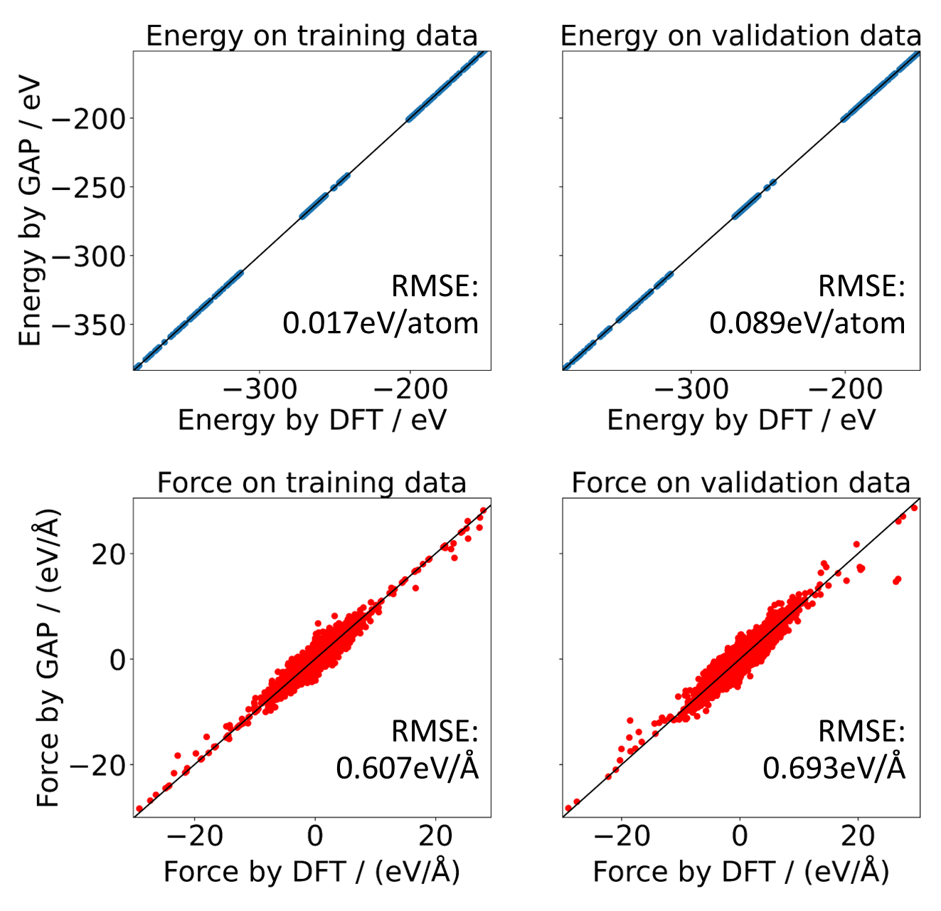
Later, the quality of the trained GAP model is assessed by comparing the obtained energies per atom and forces of samples in the training and validation sets with the trained GAP model and DFT calculations. Significantly low root-mean-squared-errors (RMSE) values are obtained for training and validation sets as presented in 1. A slightly higher RMSE for the validation set is expected since those structures are not used for training the model. Low RMSE values show a good agreement between the GAP model and DFT calculations.
2.2 Molecular Dynamics Simulations
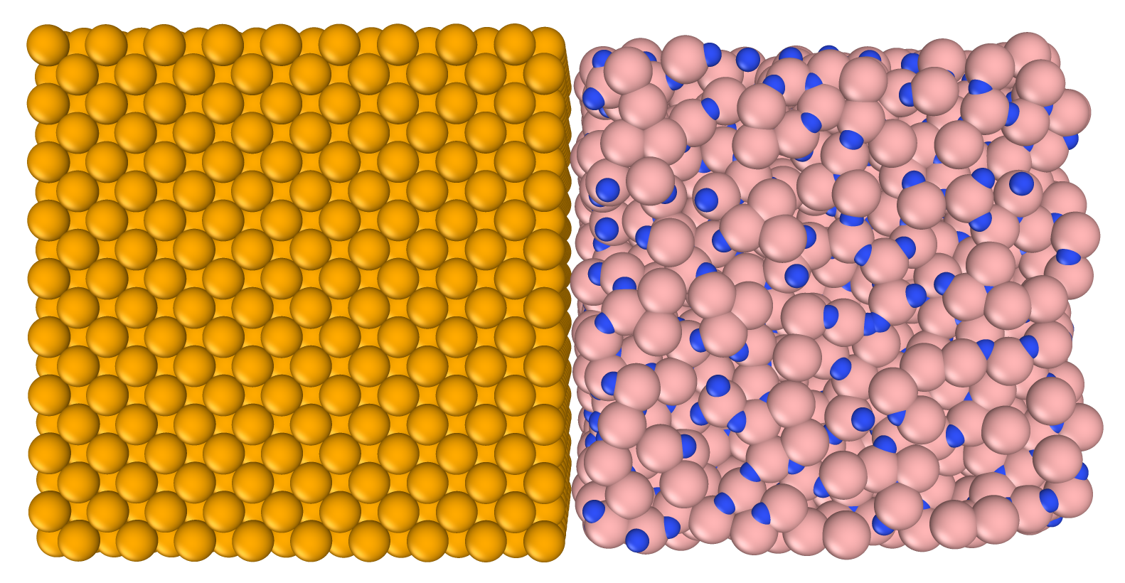
To evaluate the barrier properties of -BN samples, we generated various samples with different thicknesses varying from 3 nm to 7 nm using the melt-quenched protocol. Here, we first heat the randomly positioned BN atoms at random positions to 5000 K and later reduce the temperature to 300 K employing varying cooling rates. After the quenching, we also employ annealing steps to reduce the amount of homonuclear bonds and other impurities. By employing the cooling rates, we achieve different morphologies which allows us to understand how the morphology affects the barrier properties. After the generation of samples, the morphological (amounts of and , amount of homonuclear bonds, nanovoids) and mechanical properties are evaluated. After the structural characterization, we put the -BN samples between two [0001] cubic Cu layers which are 5 nm thick. Here, the interactions between aBN and Cu atoms are calculated using a newly developed GAP model. Fig. 2 shows a sample structure used in this paper. All of the simulations are carried out by the Large-scale Atomic/Molecular Massively Parallel Simulator (LAMMPS) package [30].
2.3 Experimental Studies
2.3.1 -BN Film Growth
To experimentally demonstrate the barrier properties of aBN samples, we employed capacitively coupled plasma-chemical vapor deposition (CCP-CVD) to deposit aBN films. The Si substrate was placed on a substrate holder in the deposition chamber. The substrate was heated at a rate of 10 ºC/min and reached growth temperatures between 350 and 400 ºC. Following a 20-minute annealing process, a borazine precursor (, Gelest) was introduced into the chamber at a rate of 0.05 sccm with a hydrogen flow of 20 sccm. During the growth process, the plasma operated at a power of 20 W. The growth time was adjusted between 20 and 80 minutes depending on the thickness of the aBN film. After the growth was completed, the furnace was slowly cooled down to room temperature.
2.3.2 Experimental Cu Diffusion Barrier Test
We assessed the Cu diffusion barrier properties of the grown aBN films. For comparison with simulation results, 3-nm, 5-nm, and 7-nm thick aBN films on Si substrate were prepared and a 50-nm thick Cu film was deposited on aBN/Si by e-beam evaporation. Cu/aBN/Si samples were annealed at the temperature range of 400 ºC to 600 ºC for 30 minutes using a vacuum furnace. Subsequently, these samples were immersed in a Cu etchant (49-1, Trensene) for 20 minutes to remove the Cu films, followed by a deionized water rinse. to remove the excess etchant. Cu diffusion was evaluated through confirmation of the formation of copper silicide using X-ray diffraction (XRD) and scanning electron microscopy (SEM).
3 Results and Discussion
3.1 Molecular Dynamics Simulations
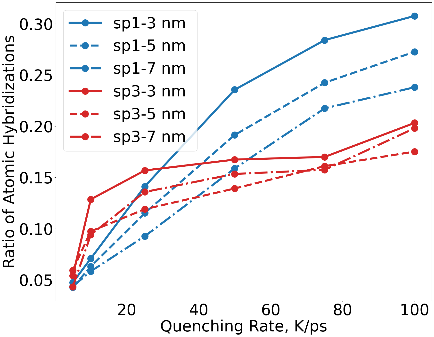
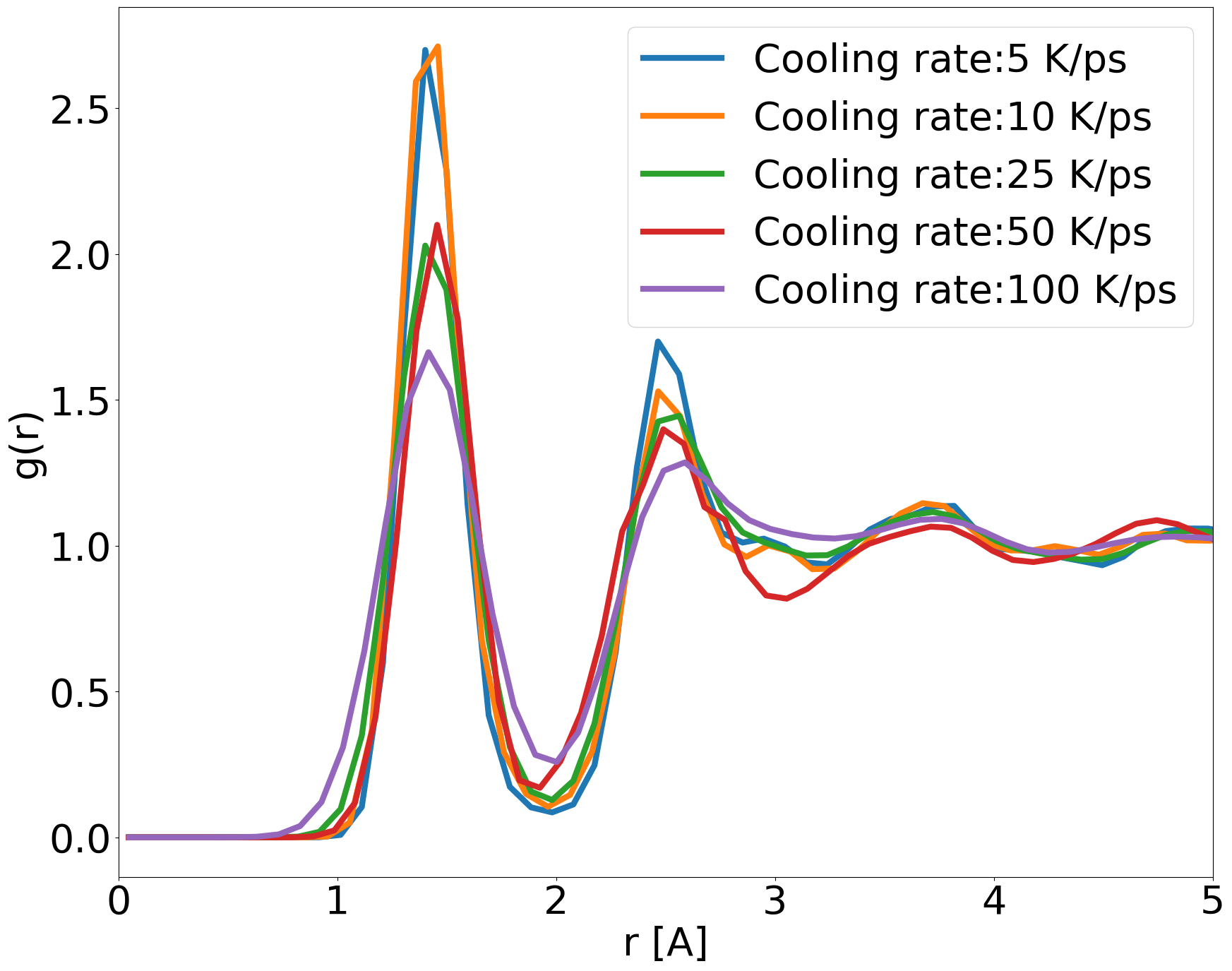
Before studying the barrier properties, a rigorous morphological investigation was carried out for MQ samples to understand how different fabrication conditions change the morphology of -BN samples. Fig. 3 presents how the amount of , , and homonuclear bonds change with the different cooling rates. As cooling rates are getting higher, atoms cannot find enough to organize in an ordered way and are trapped in a disordered state. Hence, fasting cooling rates lead to more disordered samples with higher amounts of homonuclear bonds and hybridized atoms, which may adversely affect the stability of the films. On the contrary, slowly cooled -BN samples tend to have a high amount hybridized atoms and a low amount of homonuclear bonds. Even though -hybridized atoms do not adversely affect the stability of the films, they also diminish with the slower cooling. The annealing step can help atoms reorganize themselves and generate a more ordered structure. However, as shown in Fig. 3, the samples generated with high cooling rates still have higher homonuclear bonds and . The difference between the bonding structure of films generated with different cooling rates can be observed in the first peak of RDF in Fig.4. While slowly cooled down samples have a narrower peak around 1.42 , average length of B-N bonds, fastly cooled down samples have broader peaks due to the presence of shorter and longer B-N bonds, and the presence of N-N and B-B bonds, which have average bond lengths of 1.4 and 1.81 , respectively. RDF also reveals the amorphicity of the samples can vary by employing different cooling rates. Additionally, samples cooled down faster tend to have nanovoids which may provide extra pathways for Cu atoms diffusion. While samples cooled down slower have a density around 2.18 or higher, samples quenched fast have a lower density which is caused by the nanovoids and other defects in the sample.
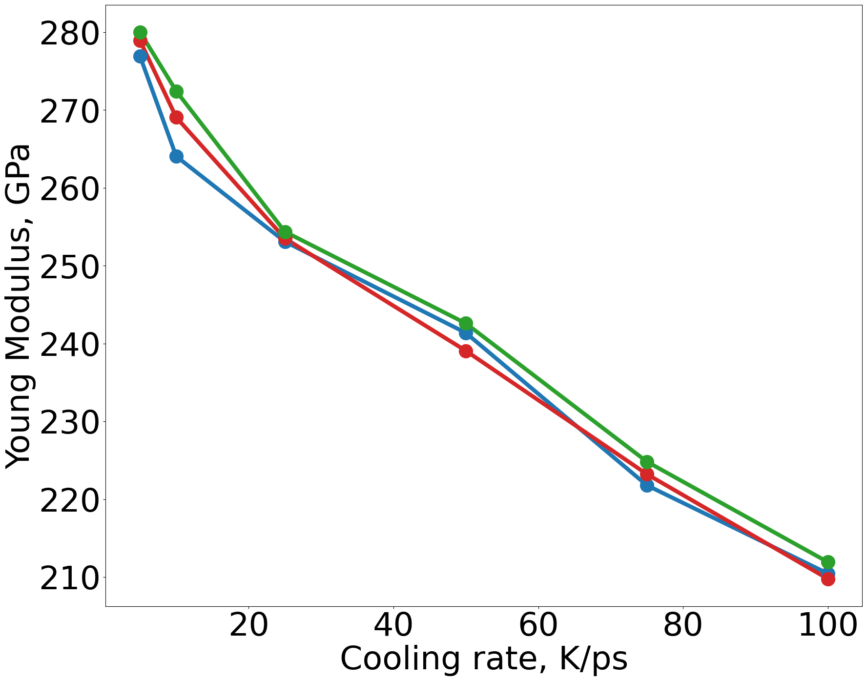
After the structural characterization, the full elastic stiffness matrix of generated -BN samples is calculated by using the stress fluctuations and the second derivatives of the energy with respect to the strain, i.e. Born matrix. Young’s modulus of generated -BN samples with different thicknesses are presented in Fig. 5. Results show that fast-cooled -BN samples with high amounts of -hybridized atoms and homonuclear bonds have lower Young’s modulus. Larger amounts of and less homonuclear bonds have higher density and Young’s modulus which is desired for diffusion barrier. While fast-cooled samples have Young’s modulus of 206 GPa, Young’s modulus of slowly cooled samples may be as high as 280 GPa. Similar trends are observed in the literature [14, 17, 18, 31]. Good mechanical properties and stability are crucial for future barrier materials and dielectrics which makes them more suitable for integration.
Finally, we create -BN/Cu heterostructures to understand the barrier properties of the films. Hence, the diffusivity of Cu atoms is extracted from the mean-squared displacement (MSD). This helps us to evaluate the thermal stability of -BN samples and how Cu atoms can penetrate through the barrier. The positions of atoms are printed at every 10 fs and visualized using a visualization tool, OVITO[32]. We later calculate the MSD by evaluating the displacement of atoms relative to their initial positions. Fig. 6 shows the diffusivity of Cu atoms as a function of temperature. As shown in Fig. 6-a, all 7-nm-thick films can stop Cu diffusion regardless of the density of -BN films up to 1000 K which exceeds the expectation of the interconnect industry. 7-nm-thick films have a more ordered structure due to the high amount of -hybridized atoms and fewer homonuclear bonds compared to the thinner films cooled with the same cooling rates and quenching protocol. A high amount of and hybridized bonds improve the thermal stability of films, and reduce the cracks or nanovoids that create pathways to Cu atoms. The and dominated samples with low amounts of homonuclear bonds, along with the large thickness, can prevent the Cu atoms from diffusing to -BN films and then to the other Cu region. Even though thicker films are better diffusion barriers, the dielectric constant can be higher for thicker films which can increase the RC delay and prevent further down-scaling of the devices. We also calculated the diffusivity of Cu through thinner a-BN as shown in Fig. 6-b and c where the data shows that the diffusivity depends largely on the morphology.
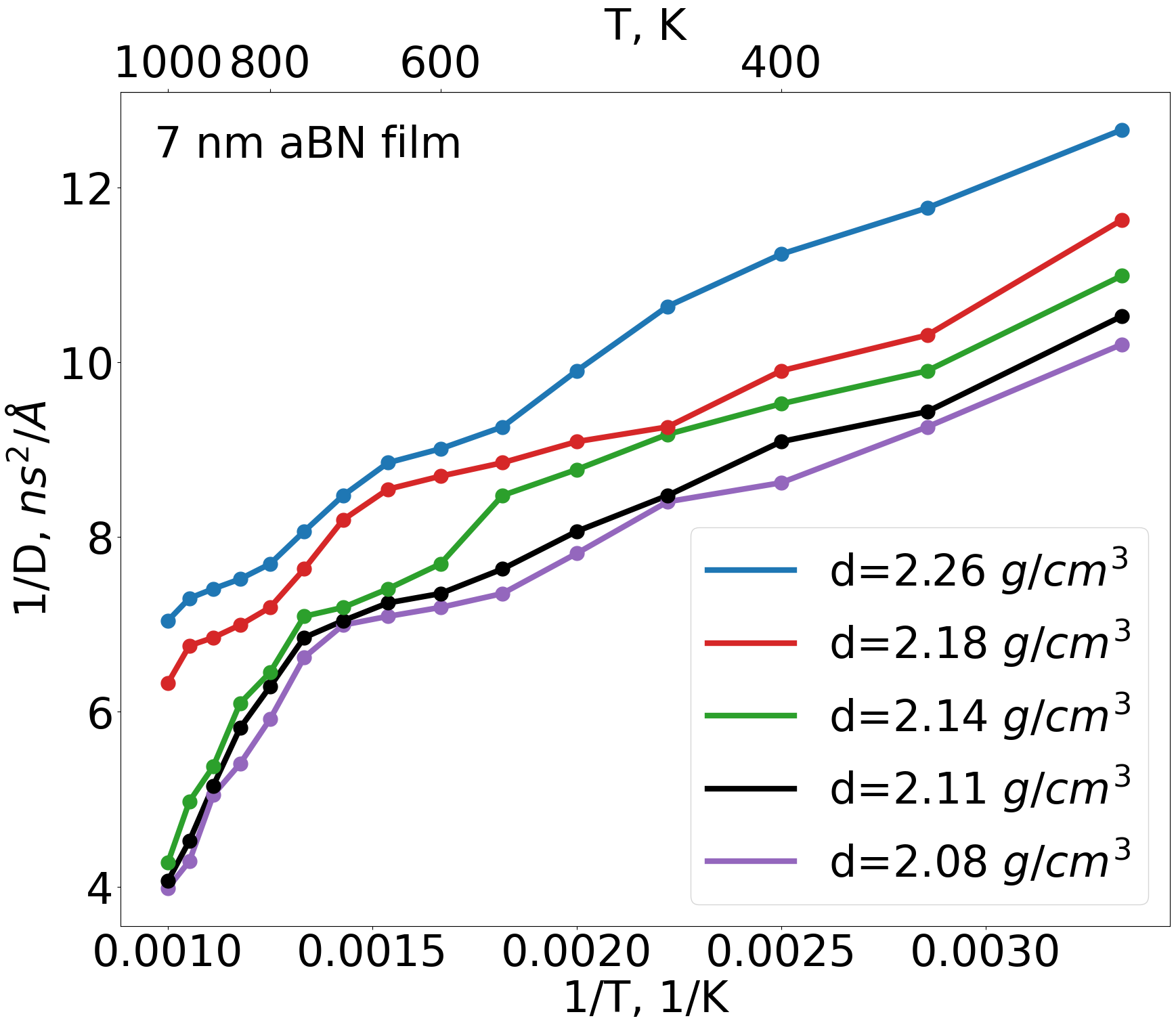
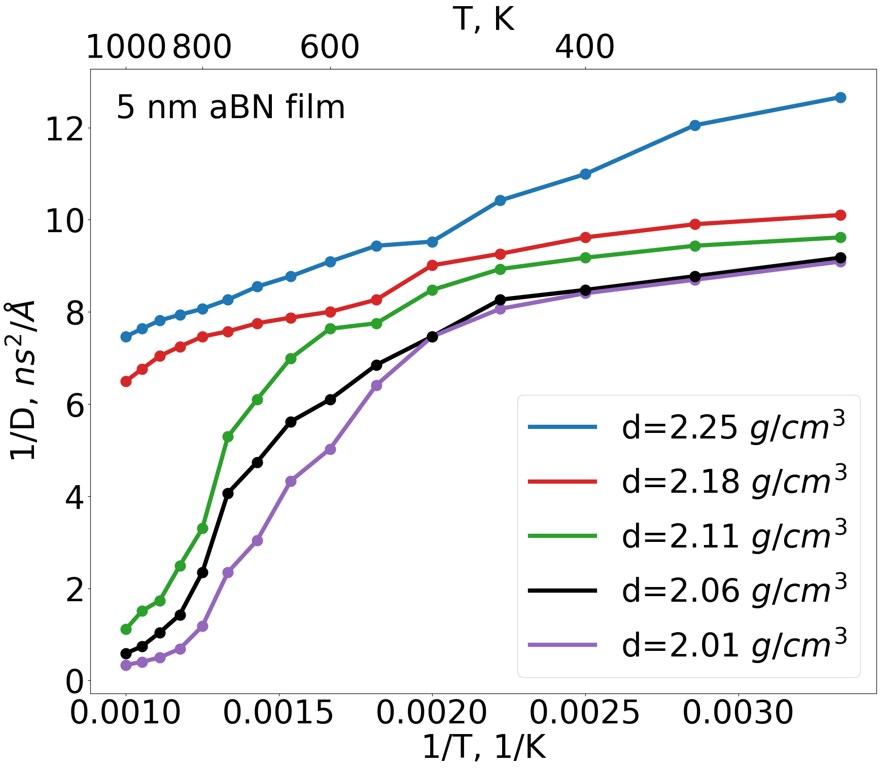
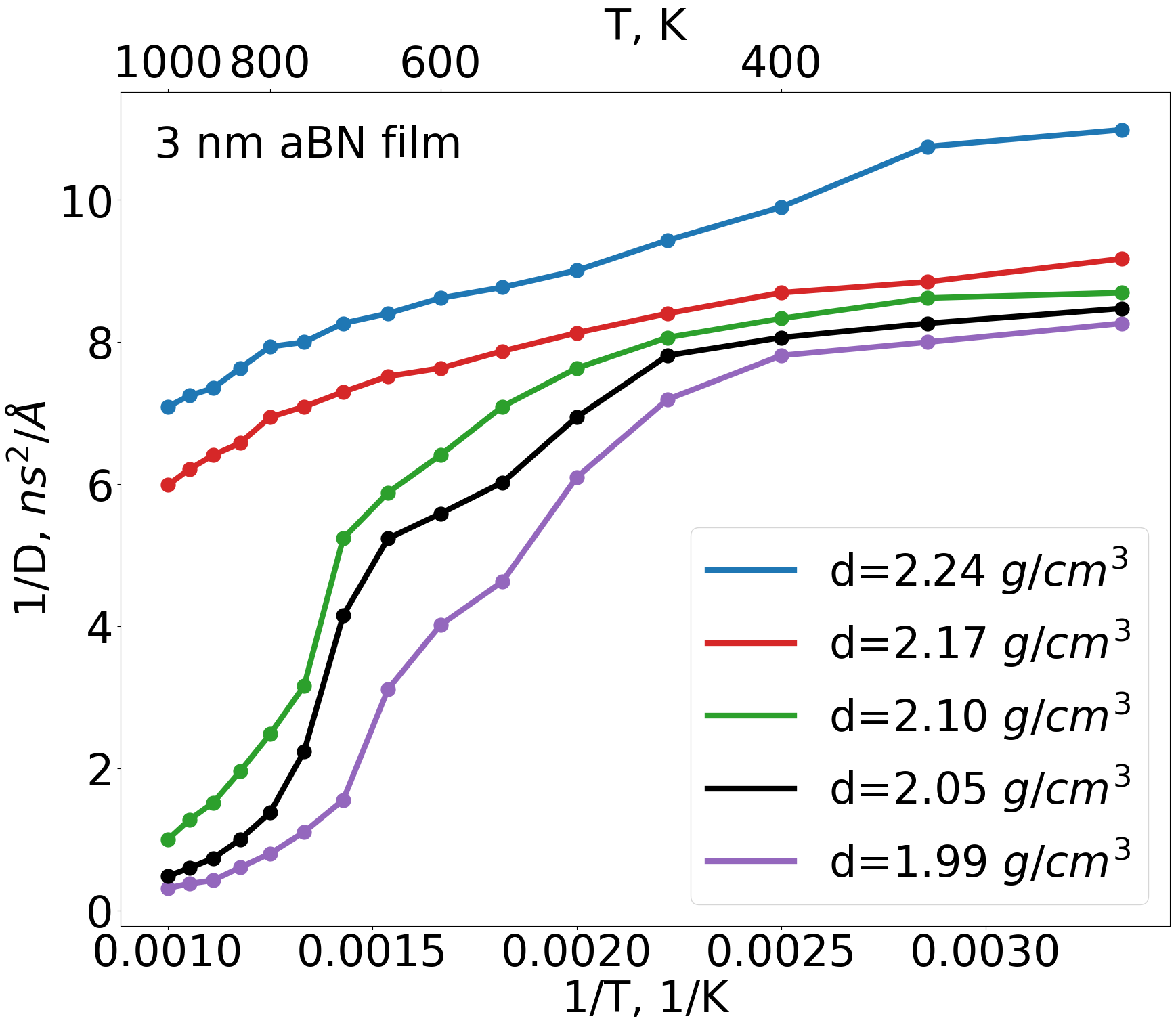
As shown earlier above, the variation of atom hybridizations and bond types of 3-nm and 5-nm films are more sensitive to the cooling process compared to 7-nm thick films. These films have more -hybridized atoms and homonuclear bonds compared to 7-nm films, and some have nanovoids and cracks which might be detrimental to the barrier properties. Fig. 6-b and c show that films with higher density, less , and homonuclear bonds can be better diffusion barriers than the thicker films suggesting that the thinner films might meet or exceed the Cu-barrier requirements at the industrial relevant thermal budgets. Analogous to the mechanical properties and amount of -hybridized atoms, both 3-nm and 5-nm films with the highest density have better Cu diffusion barrier properties up to 1000K. These structures have only a negligible amount of B-Cu or N-Cu bonds (mostly near the -BN/Cu interface) and -hybridized atoms (3-5%) and a significant amount of -hybridized atoms (10-14%). The positive impact of -hybridized atoms on the stability is already shown in the literature[17, 18]. Even though a certain amount of -hybridized atoms increases the density and decreases the voids, it should be noted that a high amount of non--hybridized may lead to some internal stress which would be the main cause of the nanovoids we observed in fast cooled samples. Moreover, higher hybridization and density, even though it may improve the diffusion barrier performance of the film, may cause to formation of additional conductive pathways and increase the dielectric constant of the material [11]. Since a higher dielectric constant of -BN would increase the RC delay of the device, the impact of the -hybridizations on electronic and optical properties should be investigated thoroughly.
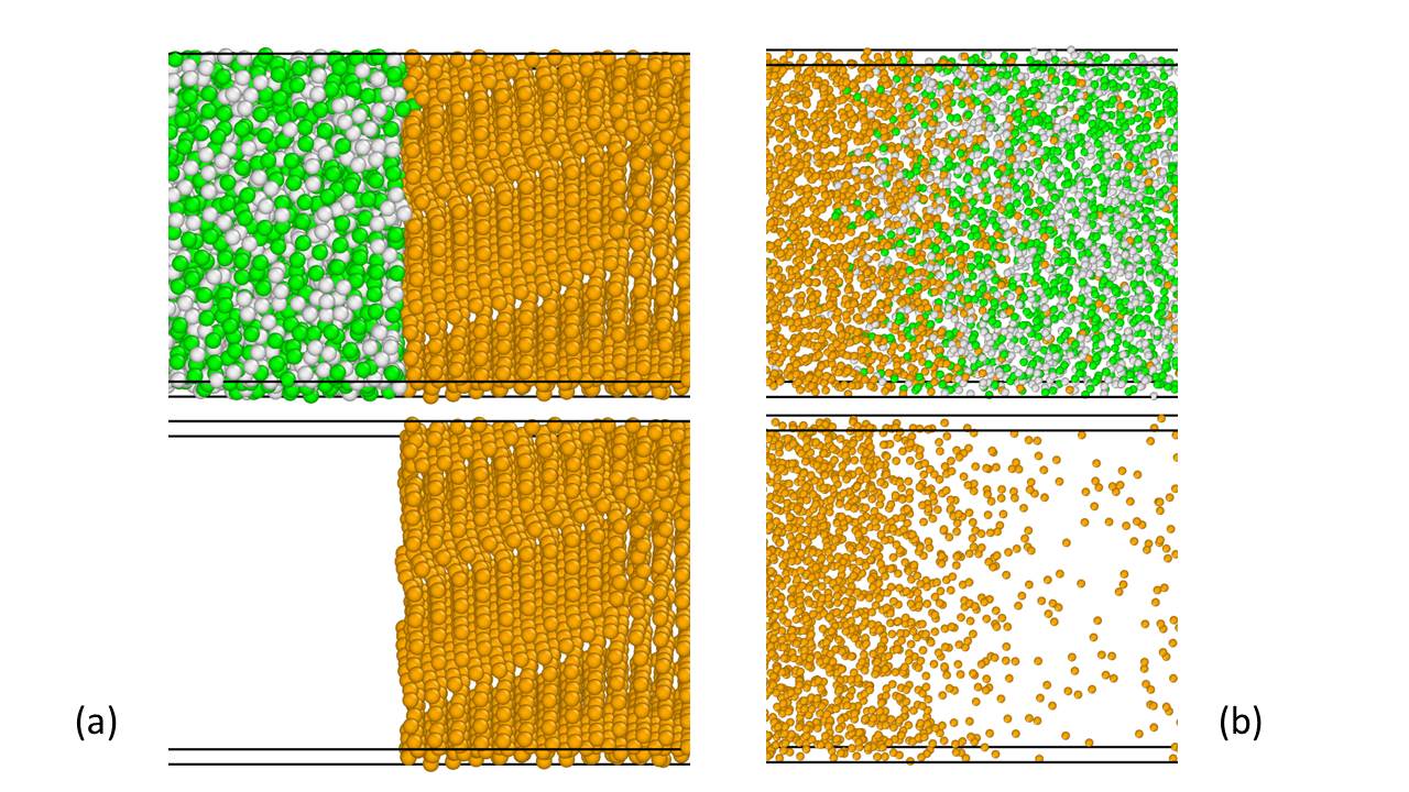
Despite the positive impact of -hybridized atoms on the barrier performance of high-density samples (blue lines in Fig.6-b and -c), nearly full -hybridized B-N network are very effective in stopping the Cu diffusion (as shown the red straight lines in Fig.6-b and -c). Both these samples have the slowest quenching rate during the sample generation and have insignificant amounts of non--hybridized atoms or homonuclear bonds. Although some Cu atoms manage to diffuse to these samples, they could only diffuse to the near-interface region since B-N network may not have sufficient Cu-diffusion pathways. As expected, due to low stability and extra diffusion pathways formed by cracks and nanovoids, Cu atoms could easily diffuse to the fast-cooled -BN. Fig. 7 visualizes how Cu atoms diffuse into the two -BN films generated with different cooling rates at 800 K. The -BN film in Fig.7-a (d=2.17 in Fig.6-c) in the figure is cooled slowly, hence it has mostly B-N and -hybridized atoms, and nearly no nanovoids. This film could stop Cu diffusion up to 1000 K, only then it allows only a small number of Cu atoms could penetrate through the -BN film. Meanwhile, the film in 7-b (d=1.99 in Fig.6-c) is cooled fast and has substantial amount of homonuclear bonds, -hybridized atoms and nanovoids. This film could not stop the Cu diffusion at lower temperature and lost its structural integrity at 800 K completely and Cu atoms completely diffuse to the film.
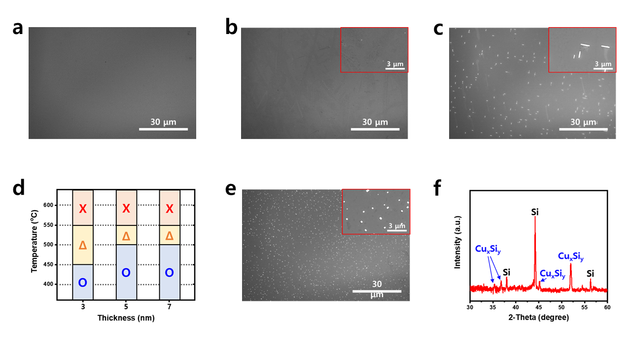
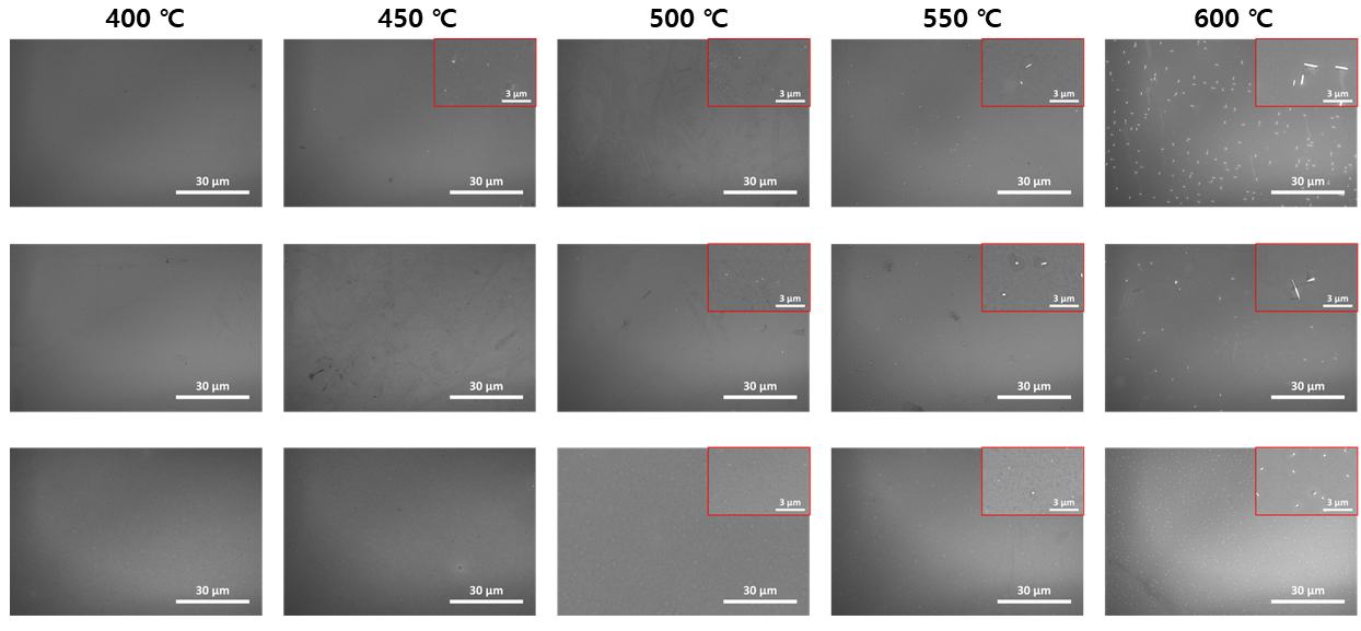
To experimentally evaluate the Cu diffusion barrier properties of aBN, we fabricated Cu/aBN/Si structures and annealed them at 400 - 600 ℃ for 30 minutes. After annealing at 400 ℃, a Si substrate coated with a 3-nm thick aBN film did not form any copper silicide (Fig. 8-a), while a Si substrate not covered with aBN formed a substantial amount of copper silicide (Fig. 8-e). After annealing 3-nm thick aBN/Si at 500 ℃, very small copper silicide nucleations were observed on the Si surface (Fig. 8-b), and it was confirmed that the formation of copper silicide crystals after annealing at 600 ℃ (Fig. 8-d). Fig. 8-c provides a brief summary of Cu diffusion barrier properties of 3-nm, 5-nm, and 7-nm thick aBN films after the 400 - 600 ℃ annealing process. The observation of crystallization by SEM is fine but not sensitive enough to determine Cu diffusion in the sub-silicide formation regime - that is - you could have Cu in the Si but SEM resolution is insufficient to detect or within the solubility limit of Cu in Si (Fig. 9). The characteristics such as density or existence of defects of experimentally synthesized aBN films differ from the simulated aBN films and do not exhibit the same barrier performance as the simulations. However, there is a tendency for the barrier property to improve as the thickness of the aBN film increases.
4 Conclusion
In summary, this study reports a comprehensive analysis that underscores the potential of -BN as an effective Cu diffusion barrier that could be used for future-generation integrated circuits to meet the ever-demanding RC-delay time constant. MD simulations with Gaussian Approximation Potential (GAP) modeling have allowed for a nuanced understanding of how different morphologies of -BN influence its barrier properties. Complementing the theoretical insights, our experimental investigations confirm the efficacy of -BN films to act as significant resistance for blocking copper migration. Such findings demonstrate that -BN films exhibit an efficient barrier against copper diffusion and hence respond to a major challenge for BEOL integration of metal wiring. This work not only contributes to the evolving landscape of material science in nanoelectronics but also sets a precedent for future research, which should focus on fine-tuning the properties of -BN and exploring its integration into existing semiconductor manufacturing processes.
Finally, one should add that the use of Artificial Intelligence-based techniques is the cornerstone to obtain realistic interatomic potentials or electronic models able to deliver quantitative predictions [33, 34]. This has become fundamental to achieve predictive modeling of thermal stability, mechanical [17, 18], electronic, dielectric properties [35], or other properties in amorphous forms of boron-nitride composites, enabling further materials optimization and performance improvement [36, 37].
Acknowledgement
This project has been supported by Samsung Advanced Institute of Technology and is conducted under the REDI Program, a project that has received funding from the European Union’s Horizon 2020 research and innovation programme under the Marie Skłodowska-Curie grant agreement no. 101034328. This paper reflects only the author’s view and the Research Executive Agency is not responsible for any use that may be made of the information it contains. ICN2 acknowledges the Grant PCI2021-122092-2A funded by MCIN/AEI/10.13039/501100011033 and by the “European Union NextGenerationEU/PRTR”. Simulations were performed at the Texas Advanced Computing Center (TACC) at The University of Texas at Austin and the Center for Nanoscale Materials, a U.S. Department of Energy Office of Science User Facility, supported by the U.S. DOE, Office of Basic Energy Sciences, under Contract No. DE-AC02-06CH11357.
References
References
- [1] Shamiryan D, Abell T, Iacopi F and Maex K 2004 Materials Today 7 34–39 ISSN 1369-7021 URL https://www.sciencedirect.com/science/article/pii/S1369702104000537
- [2] Hong S, Lee C S, Lee M H, Lee Y, Ma K Y, Kim G, Yoon S I, Ihm K, Kim K J, Shin T J, Kim S W, chae Jeon E, Jeon H, Kim J Y, Lee H I, Lee Z, Antidormi A, Roche S, Chhowalla M, Shin H J and Shin H S 2020 Nature 582(7813) 511–514 ISSN 1476-4687 URL https://doi.org/10.1038/s41586-020-2375-9
- [3] Liu J, Loh K P, Lin M, Foo Y L, Wang W D and Chi D Z 2004 Journal of Applied Physics 96 6679–6684 ISSN 0021-8979 (Preprint https://pubs.aip.org/aip/jap/article-pdf/96/11/6679/14681778/6679_1_online.pdf) URL https://doi.org/10.1063/1.1808909
- [4] Deijkers J S H, de Jong A A, Mattinen M J, Schulpen J J P M, Verheijen M A, Sprey H, Maes J W, Kessels W E M M, Bol A A and Mackus A J M 2023 Advanced Materials Interfaces 10 2202426
- [5] Zhao R, Lo C L, Zhang F, Ghosh R K, Knobloch T, Terrones M, Chen Z and Robinson J 2019 Advanced Materials Interfaces 6 1901055 (Preprint https://onlinelibrary.wiley.com/doi/pdf/10.1002/admi.201901055) URL https://onlinelibrary.wiley.com/doi/abs/10.1002/admi.201901055
- [6] Maestre C, Toury B, Steyer P, Garnier V and Journet C 2021 Journal of Physics: Materials 4 044018 URL https://dx.doi.org/10.1088/2515-7639/ac2b87
- [7] Ranjan A, O’Shea S J, Padovani A, Su T, La Torraca P, Ang Y S, Munde M S, Zhang C, Zhang X, Bosman M, Raghavan N and Pey K L 2023 ACS Applied Electronic Materials 5 1262–1276
- [8] Jiang L, Shi Y, Hui F, Tang K, Wu Q, Pan C, Jing X, Uppal H, Palumbo F, Lu G, Wu T, Wang H, Villena M A, Xie X, McIntyre P C and Lanza M 2017 ACS Applied Materials & Interfaces 9 39758–39770 pMID: 29039199
- [9] Ahmed M, Li Y, Chen W and Li E P 2022 Nanotechnology 33 165201 URL https://dx.doi.org/10.1088/1361-6528/ac4879
- [10] Glavin N R, Jespersen M L, Check M H, Hu J, Hilton A M, Fisher T S and Voevodin A A 2014 Synthesis of few-layer, large area hexagonal-boron nitride by pulsed laser deposition vol 572 (Elsevier B.V.) pp 245–250 ISSN 00406090
- [11] Glavin N R, Muratore C, Jespersen M L, Hu J, Hagerty P T, Hilton A M, Blake A T, Grabowski C A, Durstock M F, McConney M E, Hilgefort D M, Fisher T S and Voevodin A A 2016 Advanced Functional Materials 26(16) 2640–2647 URL https://onlinelibrary.wiley.com/doi/abs/10.1002/adfm.201505455
- [12] Sattari-Esfahlan S M, Kim H G, Hyun S H, Choi J H, Hwang H S, Kim E T, Park H G and Lee J H 2023 ACS Applied Materials and Interfaces 15(5) 7274–7281 ISSN 19448252
- [13] Chen C Y, Sun Z, Torsi R, Wang K, Kachian J, Liu B, Rayner Jr G B, Chen Z, Appenzeller J, Lin Y C et al. 2023 arXiv preprint arXiv:2312.09136
- [14] Lin C M, Hsu C H, Huang W Y, Astié V, Cheng P H, Lin Y M, Hu W S, Chen S H, Lin H Y, Li M Y, Magyari-Kope B, Yang C M, Decams J M, Lee T L, Gui D, Wang H, Woon W Y, Lin P, Wu J, Lee J J, Liao S S and Cao M 2022 Advanced Materials Technologies 7(10) 2200022 URL https://onlinelibrary.wiley.com/doi/abs/10.1002/admt.202200022
- [15] Abbas Q, Liang H, Shi J, Chen Y, Xia X, ul Ahmad A, Liu J and Du G 2018 Materials Letters 227 284–288 ISSN 0167-577X URL https://www.sciencedirect.com/science/article/pii/S0167577X1830853X
- [16] Kim K, Kim H, Lee S W, Lee M Y, Lee G, Park Y, Kim H, Lee Y H, Kim M, Ma K Y, Kim M J, Kim T S, Shin H S and Cho B J 2023 IEEE Transactions on Electron Devices 70(5) 2588–2593 ISSN 0018-9383 URL https://ieeexplore.ieee.org/document/10079183/
- [17] Kaya O, Colombo L, Antidormi A, Lanza M and Roche S 2023 Nanoscale Horizons 8(3) 361–367 ISSN 20556764
- [18] Kaya O, Colombo L, Antidormi A, Villena M A, Lanza M, Cole I and Roche S 2023 Impact of hydrogenation on the stability and mechanical properties of amorphous boron nitride (Preprint 2310.18102)
- [19] Bartók A P, Payne M C, Kondor R and Csányi G 2010 Physical Review Letters 104(13) 136403 URL https://link.aps.org/doi/10.1103/PhysRevLett.104.136403
- [20] Bartók A P, Kondor R and Csányi G 2013 Phys. Rev. B 87(18) 184115 URL https://link.aps.org/doi/10.1103/PhysRevB.87.184115
- [21] Giannozzi P, Baroni S, Bonini N, Calandra M, Car R, Cavazzoni C, Ceresoli D, Chiarotti G L, Cococcioni M, Dabo I et al. 2009 Journal of physics: Condensed matter 21 395502
- [22] Giannozzi P, Andreussi O, Brumme T, Bunau O, Nardelli M B, Calandra M, Car R, Cavazzoni C, Ceresoli D, Cococcioni M et al. 2017 Journal of physics: Condensed matter 29 465901
- [23] Giannozzi P, Baseggio O, Bonfà P, Brunato D, Car R, Carnimeo I, Cavazzoni C, De Gironcoli S, Delugas P, Ferrari Ruffino F et al. 2020 The Journal of Chemical Physics 152 154105
- [24] Tkatchenko A and Scheffler M 2009 Phys. Rev. Lett. 102(7) 073005 URL https://link.aps.org/doi/10.1103/PhysRevLett.102.073005
- [25] Freire R L H, Guedes-Sobrinho D, Kiejna A and Da Silva J L F 2018 The Journal of Physical Chemistry C 122 1577–1588 (Preprint https://doi.org/10.1021/acs.jpcc.7b09749) URL https://doi.org/10.1021/acs.jpcc.7b09749
- [26] Thiemann F L, Rowe P, Müller E A and Michaelides A 2020 The Journal of Physical Chemistry C 124 22278–22290 (Preprint https://doi.org/10.1021/acs.jpcc.0c05831) URL https://doi.org/10.1021/acs.jpcc.0c05831
- [27] Deringer V L and Csányi G 2017 Physical Review B 95(9) ISSN 24699969
- [28] Deringer V L, Bartók A P, Bernstein N, Wilkins D M, Ceriotti M and Csányi G 2021 Gaussian process regression for materials and molecules
- [29] Mahoney M W and Drineas P 2009 Proceedings of the National Academy of Sciences 106 697–702
- [30] Thompson A P, Aktulga H M, Berger R, Bolintineanu D S, Brown W M, Crozier P S, in ’t Veld P J, Kohlmeyer A, Moore S G, Nguyen T D, Shan R, Stevens M J, Tranchida J, Trott C and Plimpton S J 2022 Comp. Phys. Comm. 271 108171
- [31] Lehmann G, Hess P, Wu J J, Wu C T, Wong T S, Chen K H, Chen L C, Lee H Y, Amkreutz M and Frauenheim T 2001 Phys. Rev. B 64(16) 165305 URL https://link.aps.org/doi/10.1103/PhysRevB.64.165305
- [32] Stukowski A 2010 Modelling and Simulation in Materials Science and Engineering 18 ISSN 0965-0393
- [33] Schleder G R, Padilha A C M, Acosta C M, Costa M and Fazzio A 2019 Journal of Physics: Materials 2 032001 URL https://dx.doi.org/10.1088/2515-7639/ab084b
- [34] Li W, Chen P, Xiong B, Liu G, Dou S, Zhan Y, Zhu Z, Chu T, Li Y and Ma W 2022 Journal of Physics: Materials 5 014003 URL https://dx.doi.org/10.1088/2515-7639/ac5914
- [35] Galvani T, Hamze A K, Caputo L, Kaya O, Dubois S, Colombo L, Nguyen V H, Shin Y, Shin H J, Charlier J C and Roche S 2024 Exploring dielectric properties in models of amorphous boron nitride (Preprint 24XXXXX)
- [36] Matsoso B J, Garcia-Martinez C, Mongwe T H, Toury B, Serbena J P M and Journet C 2021 Journal of Physics: Materials 4 044007 URL https://dx.doi.org/10.1088/2515-7639/ac09d4
- [37] Molina-Garcia M A, Bellani S, Castillo A E D R, Conticello I, Gabatel L, Zappia M I, Eredia M, Thorat S, Martin-Garcia B, Ceseracciu L, Piccinni M and Bonaccorso F 2023 Journal of Physics: Materials 6 035006 URL https://dx.doi.org/10.1088/2515-7639/acd0d8