shapes
Multicols Demo
High-Performance Data Mapping for BNNs on PCM-based Integrated Photonics
Abstract
State-of-the-Art (SotA) hardware implementations of Deep Neural Networks (DNNs) incur high latencies and costs. Binary Neural Networks (BNNs) are potential alternative solutions to realize faster implementations without losing accuracy. In this paper, we first present a new data mapping, called TacitMap, suited for BNNs implemented based on a Computation-In-Memory (CIM) architecture. TacitMap maximizes the use of available parallelism, while CIM architecture eliminates the data movement overhead. We then propose a hardware accelerator based on optical phase change memory (oPCM) called EinsteinBarrier. EinsteinBarrier incorporates TacitMap and adds an extra dimension for parallelism through wavelength division multiplexing, leading to extra latency reduction. The simulation results show that, compared to the SotA CIM baseline, TacitMap and EinsteinBarrier significantly improve execution time by up to 154 and 3113, respectively, while also maintaining the energy consumption within 60% of that in the CIM baseline.
I Introduction
Developments in Deep Neural Network (DNN) in the past decade have led to significant improvements in accuracy and execution time of computer vision tasks [1, 2, 3]. However, current DNN hardware implementations are relatively slow and costly to run [4, 5] due to data movement overhead and expensive GPUs [6]. Hence, developing high-throughput, cost-effective hardware for DNNs while maintaining accuracy is critical.
Recently, researchers have proposed the use of simpler (operation-wise) and smaller Neural Networks (NNs) such as Binary Neural Networks (BNNs). BNNs offer near State-of-the-Art (SotA) accuracy on vision tasks [7] and enjoy lower memory requirements (binary values or vectors of {0, 1} or {-1, 1}) [5, 8] and simplified arithmetic operations (XNOR instead of multiplication or convolution) [7]. However, BNNs on traditional systems using GPUs incur high data movement overhead [7, 9, 10].
The Computation-In-Memory (CIM) paradigm, especially as implemented with photonics and optical hardware, allows the data movement overhead to be alleviated while also achieving high throughput for BNNs and DNNs [11, 12, 13]. However, the previous CIM works that try to alleviate this overhead [14, 15] fail to (fully) exploit the inherent features of the underlying hardware as they (a) lack efficient data mapping, (b) perform at most one single vector operation (e.g., Vector-Matrix-Multiplication (VMM) or logical vector operation that is the most common operation in NNs) at a time, which limits the throughput, and (c) face many design challenges such as crosstalks and large capacitances of the wiring within the memory IP of CIM, which make the design of such devices complex and limits their scalability. Even in the case of photonic CIM, it has been shown that at high frequencies (i.e., high noise level), recovering the result in a CIM architecture comes at a high cost and reduced accuracy [16]. Fortunately, using a smaller bit count leads to an increase in the robustness, offering an opportunity for CIM architectures in photonics with high frequencies [16, 17].
Our paper advances the SotA CIM accelerators for BNNs by providing a high throughput accelerator based on an oPCM crossbar combined with an efficient mapping method tuned to maximize the parallelism. The proposed accelerator realizes an order of magnitude improvement in latency/throughput. The main contributions of the paper are:
-
•
TacitMap: A highly parallel data mapping for BNN operations on any CIM design capable of performing VMM, e.g., memristor-based crossbars based on electronic phase change memory (ePCM) or resistive random-access memory (ReRAM). TacitMap is designed with the conventional 1T1R memory crossbar structure in mind and is therefore compatible with many of the already evolving crossbar architectures.
-
•
EinsteinBarrier: An oPCM-based CIM implementation incorporating the TacitMap mapping. EinsteinBarrier ensures maximum parallelism through exploring the potential provided by the features of CIM architecture and the inherent properties of oPCM (via wavelength division multiplexing (WDM)).
We extensively evaluate TacitMap and EinsteinBarrier and compare them with SotA implementations for various BNNs. Our results show that TacitMap improves the latency by up to 154, compared to the SotA data mapping on CIM architecture for BNNs. When exploiting oPCM and TacitMap, EinsteinBarrier improves the latency by up to 3113, compared to the same baseline.
II Background, Related Work, and Motivation
This section briefly touches on the necessary background for our work. We refer the reader to some previous works [18, 7, 6, 13] for detailed information.
II-A Computation-In-Memory for NNs
Computation-In-Memory (CIM) is a promising computing paradigm that advocates avoiding unnecessary data movement and redesigning systems that are no longer processor-centric. Previous works [19, 20, 21, 22, 23, 24, 25] show the potential of CIM architectures based on nanoscale emerging memory technologies for various applications ranging from NN-based applications to those in the genomics realm. Fig. 1 shows how a memristor-based crossbar supports Vector-Matrix-Multiplication (VMM) operations, the most dominant operation in NNs [26, 27, 28].
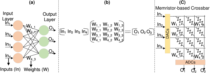
For a memristor-based crossbar (Fig. 1-(c)) to support VMM, one first maps the weight matrix in Fig. 1-(b) to conductances of the memristor devices in the crossbar. Then, they apply the input vector of indexed as voltages to the digital to analog converter (DAC) connected to the wordlines of each row in the crossbar. Based on Kirchhoff’s and Ohm’s law, a current equivalent to accumulated current for element-wise multiplication of individual and corresponding inputs and weights in a column reaches each analog to digital converter (ADC). Thus, each column performs a Multiply-and-Accumulate (MAC) operation in the analog domain, providing us with a VMM operation across multiple columns. Since the columns can work simultaneously, the VMM has an O(1) time complexity in this design.
II-B Binary Neural Network
A BNN works with binarized weights and activations (e.g., {-1, 1} or {0, 1}) instead of datatypes with higher precision, offering two advantages [5, 7]: (1) reduced storage requirement of the NN, and (2) converting the MAC operation from high-resolution multiplication and addition to a low-cost and simpler XNOR followed by an Popcount operation [7] as shown in Equation 1. In Equation 1 is convolution, is XNOR, Popcount (or population count) of a vector or specific value is the process of finding the number of set bits (1s) in that vector/value, and vector length is the length of equally sized input () or weight () vectors.
| (1) |
Unfortunately, naively reducing both activations and weights to binary representations hurt the overall accuracy compared to high-precision (floating point or fixed point) networks. Therefore, to combat this accuracy loss, previous works [7, 5] generally follow two software-based techniques. First, tracking the updates of parameters during training via higher resolutions (floating or fixed point) while keeping the actual weights binarized. Second, using binarized activations and weights only for hidden layers and keeping the input and output layers in higher resolutions. Our proposals (Section III and Section IV) also use both methods to achieve high accuracy in inference.
II-C PCM-based Integrated Photonics
Phase Change Materials (PCMs) are currently the leading alternatives for non-volatile computation in silicon photonics-based platforms [11]. A design that combines integrated photonics with PCM is the commonly known optical phase change memory (oPCM). Compared to diffractive computing in free-space optics and previous photonic-based platforms [29, 12], oPCM-based designs offer CMOS-compatible manufacturing, higher speed, and lower energy consumption for the electronics interface. This is because conventional photonic-based platforms require large and power-hungry phase shifters for calibration and reconfiguration. Therefore, a design based on oPCM can reduce both the cost and the overall footprint of photonic cores for similar logical operations [16]. Cardoso et al. [16] showed that, with a realistic noise level, using PCM devices in a multi-level fashion hurts the accuracy of an oPCM-based design when performing scalar multiplication. However, one can avoid this problem by using fewer levels or states in PCM, such as using them in a binary state. In other words, the binary usage of PCM provides the easiest solution for differentiating between the states. This fits the requirement of vectors in BNNs.
One can also utilize oPCM in a CIM design, which offers three benefits compared to the same design with electronic-based PCM as the underlying technology:
-
•
Higher parallelization: through processing multiple vectors simultaneously using frequency space, a technique known as wavelength division multiplexing (WDM) [13].
- •
- •
III TacitMap for BNN
To support necessary operations in Equation 1 (e.g., XNOR and Popcount) for hidden layers, we propose a data mapping for BNNs, called TacitMap. TacitMap requires an underlying technology inherently capable of VMM operation (Section II-A).
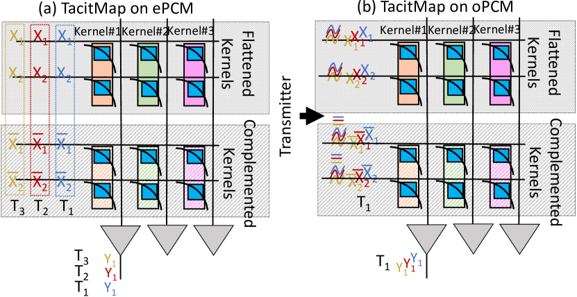
Fig. 2-(a) and -(b) present a comparison between how SotA mapping (hereafter called CustBinaryMap) [15] and TacitMap handle a single XNOR+Popcount of Equation 1, respectively. For a detailed description of CSL, BL, WL, and SL, please refer to previous works [34]. We assume input () and weight () vectors of length 2 bits. and represent the th bit of th input and weight vector, respectively. The bar on a parameter indicates its complement value. Note that the multiplication by 2 and the subtraction in Equation 1 are constant and are implemented with minimum cost on the result of either mapping.
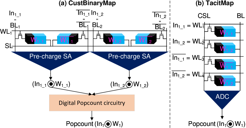
CustBinaryMap (Fig. 2-(a)) uses a 2T2R memory structure and places weight vectors horizontally in memory rows. Instead of storing the weight vectors as they are, this mapping requires the programmer to interleave the weight vectors and their complements in a bitwise manner and then store the two bits and in the two devices in the 2T2R memory cell. In contrast, TacitMap (Fig. 2-(b)) uses a 1T1R memory structure and stores each weight vector vertically in a column. In TacitMap, instead of interleaving the weight vector with its complement, one first stores the weight vector and then, right below it, stores the complemented weight vector. Regarding the inputs, CustBinaryMap does the same interleaving of the input vector and its complement with the input vectors. The outputs are read through a modified SA called precharge sense amplifier (PCSA), which is the XNOR of the input vector and stored weight vector. Conversely, TacitMap concatenates the input vector and its complement and applies it to the crossbar rows. The XNOR+Popcount is directly read out from the ADC. Although the total number of devices (i.e., memristors and transistors) is the same for both mappings, TacitMap offers three main benefits compared to CustBinaryMap:
-
•
1-step XNOR+Popcount in TacitMap compared to 2-step operation in CustBinaryMap, with no need for additional digital circuitry.
-
•
Column-wise XNOR+Popcount in TacitMap compared to row-wise operation in CustBinaryMap, enabling high parallelism for TacitMap.
- •
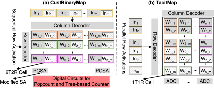
Fig. 3 presents TacitMap against CustBinaryMap at the crossbar level. We observe that TacitMap enables the crossbar to perform XNOR+Popcount via a single VMM operation in only 1 step and reads the results from ADCs simultaneously. In contrast, CustBinaryMap takes a minimum of steps for the same operations because CustBinaryMap utilizes PCSA to perform the logical XNOR for one input and one weight vector of size and processes weight vectors sequentially in steps. Moreover, CustBinaryMap also needs to perform post-processing on the read output on every final vector using two additional digital components: (1) a fully digital five-bit counter per crossbar column for local Popcount and (2) a tree-based Popcount circuit per several connected crossbars for a global Popcount. Theoretically, using the same underlying device, TacitMap should achieve up to lower execution time compared to CustBinaryMap.
Note that TacitMap is compatible with any technology for the crossbar that supports VMM, e.g., ePCM- or oPCM-based crossbars.
IV EinsteinBarrier Architecture
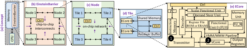
Fig. 4-(a) presents an overview of the EinsteinBarrier concept and its system placement. We envision EinsteinBarrier as an accelerator that is part of the memory itself. EinsteinBarrier is a spatial architecture (similar to PUMA [22]) with four levels: Nodes, Tiles, External Cores (ECores), and VMM-enabled cores (VCores). EinsteinBarrier extends the ISA discussed in a earlier work [22] to support multiple simultaneous VMMs, called Matrix-Matrix-Multiplication (MMM) hereafter.
EinsteinBarrier hierarchical organization, Tile architecture, and ECores provide the generality and reconfigurability needed to support various BNNs and various technologies. The ECore and the new Arch required for XNOR+Popcount brings the generality needed to support TacitMap and multiple technologies in VCores as long as they support VMM operation in a crossbar. The ECore and VCore designs prepare EinsteinBarrier in particular to adopt oPCM technology and its advantages. Finally, by simply adopting CMOS-compatible oPCM-based VCores, EinsteinBarrier avoids the challenges of ePCM-based CIM architecture (Section II-C).
IV-A oPCM-based WDM-enabled ECore
EinsteinBarrier utilizes integrated photonics with PCM devices in the crossbar. This choice of oPCM-enabled ECores demands two specific additional components, namely VCore and transmitter, compared to other CIM-enabled designs. This choice provides an extra dimension for parallelization through WDM and avoids Joule heating and resistance drift in electronic emerging memories [30, 37].
IV-A1 VCore structure
The oPCM-based VCore consists of a memory crossbar (i.e., a tile) with each cell in the crossbar being a single PCM device capable of storing 1 bit of data (binary PCM discussed in Section II-C). A tile also includes all the necessary peripheries for read and write operations (e.g., DACs and ADCs). EinsteinBarrier adds 1 more component to the readout circuitry of the oPCM core: transimpedance amplifiers (TIA) on the output (receiver). EinsteinBarrier uses TIA to feed ADCs, acting as a deserialization stage in the output.
IV-A2 WDM
Fig. 5 depicts an example to present the concept and benefits of WDM in an oPCM core. We assume 3 2-bit activation vectors of distinguished by vectors with yellow, red, and blue colors. The indices refer to the bit number. Moreover, we assume 3 2-bit kernel vectors of , where denotes the activation/kernel vector and denotes the bit position in that activation/kernel vector. Each of these kernel vectors is grouped in a box of orange, green, or pink color. The complements use the same color but striped boxes.
In Fig. 5, TacitMap requires three columns and 4 (22) rows of the crossbar to store the kernels and their complement. TacitMap requires three VMM operations111For simplicity, we assumed that the columns could be read out in parallel and they do not share an ADC. We will revisit this in Section V. to process all the required XNOR+Popcounts; i.e., 1 VMM per each activation vector, wherein each VMM we use the vector of that activation concatenated by its complement as the input to the crossbar.
Fig. 5-(a) depicts the scenario for a conventional ePCM-based VMM-enabled crossbar. In this case, the required VMMs happen in consecutive time-steps, denoted by , , and in Fig. 5-(a). The input vector size in this scenario is 4, the number of inputs is 3, and the matrix is .
On the other hand, Fig. 5-(b) depicts the same scenario but for an oPCM-based VCore. Using an optical transmitter that we discuss next, one can combine our 3 input vectors together into a single input and feed that single input to the crossbar. Therefore, only 1 time-step, i.e., , is required to finish the operation. Here, the input vector and the matrix size are still 4 and , respectively. However, the number of input vectors is reduced to 1. Therefore, effectively, WDM-enabled an MMM of size . We call the number of wavelengths that can be combined into a single wavelength and still be detectable later (with acceptable noise in TIA) the WDM capacity. Current technologies can support up to a capacity of [13], meaning a theoretical 16 improvement in performance compared to ePCM.
IV-A3 Transmitter structure
To support optical inputs and WDM, EinsteinBarrier adds a transmitter circuit ( in Fig. 4) at the ECore level feeding the VMM/MMM pipeline, where the actual oPCM-based core ( ) resides. Fig. 6 presents a high-level overview of the transmitter circuit and components.
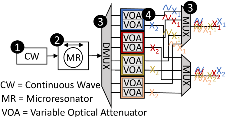
The transmitter has four main components: a laser to provide a single-wavelength continuous wave beam, a microresonator-based optical frequency comb to concentrate the optical power and excite new wavelengths based on non-linearities, DMUXs/MUXs for feeding individual waves to each variable optical attenuator (VOA) and creating a single wave carrying information on multiple bits from different vectors, and VOAs to encode the information of each input into waves via changing the amplitude. In Fig. 6, the transmitter combines four 2-bit vectors (of different colors) into a single vector of 2-bit width.
IV-B oPCM-based ECore Overheads
We showed (Section IV-A) that using oPCM provides higher parallelism (simultaneous VMMs vs. single VMM) for the same vector operations via WDM. However, this extra parallelism comes at the cost of power for the additional components. Assume a core with WDM capacity of K and crossbars of size . Such a crossbar incurs an extra power modeled by Equation 2, where N is # of TIAs, each of which consumes .
| (2) |
The transmitter power overhead is presented in Equation 3, where it accounts for the required power for the laser, modulators, and tuning [38].
| (3) |
V Evaluation Methodology
V-A Implementations and Models
We implement EinsteinBarrier as a heavily extended version of PUMA architecture and compiler [39]. This implementation222We open-source our experimental setup upon acceptance. accounts for (1) WDM capability of oPCM cores, (2) new configurations related to integrated photonics, and (3) power and area overheads introduced by extra components of oPCM cores, e.g., laser. For the photonics components, we use our device-aware extended circuits [40, 38, 13, 41]. Our ePCM-based crossbars are based on extensive characterization done in the EU project MNEMOSENE project and previous works [42, 13], generously provided to us by the partners. To evaluate additional CMOS circuitry of our design (e.g., such as MUXs), we use Synopsys Design Compiler and synthesize them in the target technology to obtain their execution time, power, and area. We apply the prominent technology scaling rules [43] to the configuration numbers of PUMA architecture to ensure our design components are based on the same technology node.
V-B Designs and Baselines
We evaluate the effectiveness of TacitMap and EinsteinBarrier separately using two different configurations: (1) TacitMap-ePCM that is TacitMap on electronic PCM-based cores, and (2) EinsteinBarrier that still uses TacitMap but utilizes oPCM-based VCores. We use two baselines: (1) the design in [15], a SotA hardware accelerator for BNNs, hereafter called Baseline-ePCM, and (2) a GPU implementation of the same network (called Baseline-GPU). We use the same PCM configuration in TacitMap-ePCM for Baseline-ePCM.
V-C Networks and Datasets
We evaluate all designs over 6 BNNs (3 convolutional networks and 3 multilayer perceptrons (MLPs)) with various sizes from MlBench [44]. We use MNIST and CIFAR-10 for the datasets. Note that neither TacitMap nor EinsteinBarrier affect the accuracy of target BNNs and simply accelerates them via efficiently handling their XNOR+Popcount in parallel.
VI Evaluation Results and Discussions
VI-A Performance Analysis
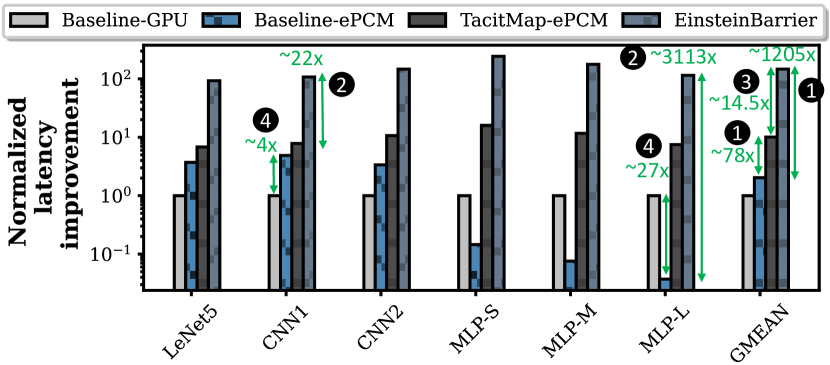
Fig. 7 presents the latency improvement of TacitMap-ePCM and EinsteinBarrier normalized to SotA. The y-axis uses a log scale. We make four key observations:
-
•
Both TacitMap-ePCM and EinsteinBarrier improve the latency over Baseline-ePCM irrespective of the underlying network. On average, TacitMap-ePCM and EinsteinBarrier improve the performance by 78 and 1205, respectively ( ). These are because, unlike the Baseline-ePCM, TacitMap-ePCM and EinsteinBarrier parallelize XNOR with Popcount and parallelize many XNOR+Popcounts via the proposed vertical data mapping.
-
•
The latency improvement is network-dependent and varies from BNN to BNN. Specifically, the latency improvements over Baseline-ePCM vary from 22 to 3113 for EinsteinBarrier ( ). This happens due to (1) the relation between the size of the hidden layers (binary layers) and the first and last layers and (2) available parallelism in the XNOR+Popcount operations of each BNN. In the evaluated BNNs, larger BNNs contain more parallel XNOR+Popcount operations.
-
•
EinsteinBarrier improves the latency on average 15 ( ) with the exact data flow compared to TacitMap-ePCM. This happens due to the extra parallelism dimension enabled by WDM and the fast crossbar read of oPCM core. This is while the improvement is still network-dependent. Unfortunately, the achieved improvement due to the technology is still lower than the WDM capacity (i.e., ). This is simply due to the underlying network, and we expect it to increase for larger networks. We leave this exploration as future work.
-
•
Baseline-ePCM does not always improve the latency over a Baseline-GPU. For example, see in Fig. 7, while Baseline-ePCM is 4 faster than Baseline-GPU for our first CNN, it is 27 slower than Baseline-GPU for our MLP-L network. This happens since in some networks, such as our MLP workloads, Baseline-ePCM has to serialize XNOR+Popcount compared to Baseline-GPU, to the extent that the benefits for reducing the data movement overhead diminish.
VI-B Energy Analysis
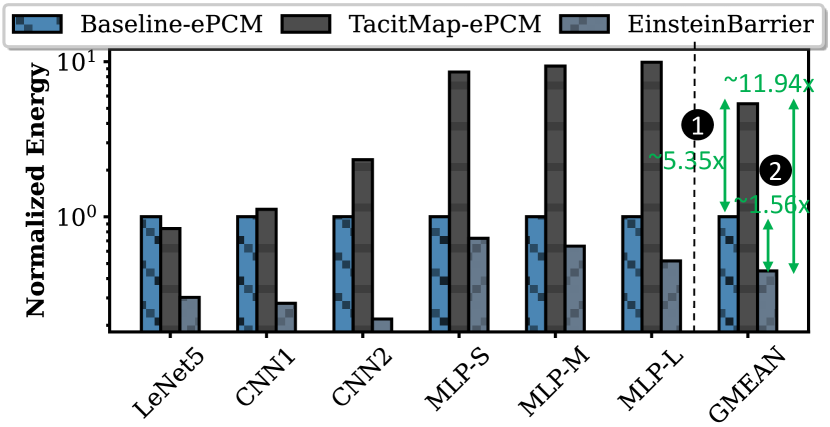
Fig. 8 compares the energy consumption of TacitMap-ePCM and EinsteinBarrier normalized to the Baseline-ePCM. The y-axis is in a log scale. We make two key observations:
-
•
On average, TacitMap-ePCM increases the energy consumption compared to Baseline-ePCM by 5.35, as TacitMap-ePCM requires power-hungry ADCs while Baseline-ePCM uses SAs ( ).
-
•
On average, EinsteinBarrier improves the energy consumption by 1.56 and 11.94 over Baseline-ePCM and TacitMap-ePCM, respectively ( ). This is achieved because EinsteinBarrier requires a lower number of crossbar activations by computing multiple outputs at the same time while using the same crossbar, ADCs, and other peripheries.
VI-C Discussions and Future Works
Multi-Level PCM Devices. Our work uses PCMs in a binary mode. However, recent works [13, 45] show the potential for multi-bit devices at the cost of increased noise. We leave extending TacitMap on multi-bit cells for future work.
Design Space Exploration of oPCM-based VCores. We evaluated EinsteinBarrier using fixed laser, array sizes, and other system configurations due to our limited access to accurate specs of different components (particularly those needed in the transmitter). A study that can freely explore this design space is encouraged and left for future work.
VII Conclusion
This paper proposes an efficient data flow for BNNs, TacitMap, and a CMOS-compatible oPCM-based hardware accelerator based on integrated photonics principles, called EinsteinBarrier, to fully exploit the possible parallelism with TacitMap. Our latency and energy evaluations suggest an average improvement of 1205 and 1.56, respectively, for BNNs on oPCM-based accelerators. This is the first step towards an optimized and efficient hardware realization for BNNs using these emerging technologies. Hence, our work encourages further investigations of oPCM in the NN realm.
References
- [1] A. Krizhevsky et al., “Imagenet classification with deep convolutional neural networks,” Communications of the ACM, 2017.
- [2] R. Girshick et al., “Rich feature hierarchies for accurate object detection and semantic segmentation,” in CVPR, 2014.
- [3] R. Girshick, “Fast r-cnn,” in ICCV, 2015.
- [4] C. Yuan et al., “A comprehensive review of binary neural network,” arXiv preprint arXiv:2110.06804, 2021.
- [5] M. Courbariaux et al., “Binaryconnect: Training deep neural networks with binary weights during propagations,” NIPS, 2015.
- [6] H. Qin et al., “Binary neural networks: A survey,” Pattern Recognition, 2020.
- [7] M. Rastegari et al., “Xnor-net: Imagenet classification using binary convolutional neural networks,” in ECCV, 2016.
- [8] I. Hubara et al., “Binarized neural networks,” NIPS, 2016.
- [9] G. Chen et al., “Phonebit: Efficient gpu-accelerated binary neural network inference engine for mobile phones,” in DATE, 2020.
- [10] E. Nurvitadhi et al., “Accelerating binarized neural networks: Comparison of FPGA, CPU, GPU, and ASIC,” in FPT, 2016.
- [11] N. Peserico et al., “Integrated photonic tensor processing unit for a matrix multiply: a review,” Journal of Lightwave Technology, 2023.
- [12] A. N. Tait, “Quantifying Power in Silicon Photonic Neural Networks,” Physical Review Applied, 2022.
- [13] J. Feldmann et al., “Parallel convolutional processing using an integrated photonic tensor core,” Nature, 2021.
- [14] Y.-F. Qin et al., “Design of high robustness BNN inference accelerator based on binary memristors,” IEEE TED, 2020.
- [15] T. Hirtzlin et al., “Digital biologically plausible implementation of binarized neural networks with differential hafnium oxide resistive memory arrays,” Frontiers in neuroscience, 2020.
- [16] R. Cardoso et al., “Towards a Robust Multiply-Accumulate Cell in Photonics using Phase-Change Materials,” in DATE, 2023.
- [17] T. Shahroodi et al., “Lightspeed Binary Neural Networks using Optical Phase-Change Materials,” in DATE, 2023.
- [18] S. Hamdioui et al., “Memristor for computing: Myth or reality?” in DATE, 2017.
- [19] T. Shahroodi et al., “RattlesnakeJake: A Fast and Accurate Pre-Alignment Filter Suitable for Computation-in-Memory,” in SAMOS, 2022.
- [20] T. Shahroodi et al., “A Case for Genome Analysis Where Genomes Reside,” in SAMOS, 2023.
- [21] A. Shafiee et al., “ISAAC: A convolutional neural network accelerator with in-situ analog arithmetic in crossbars,” ISCA, 2016.
- [22] A. Ankit et al., “PUMA: A programmable ultra-efficient memristor-based accelerator for machine learning inference,” in ASPLOS, 2019.
- [23] T. Shahroodi et al., “Demeter: A fast and energy-efficient food profiler using hyperdimensional computing in memory,” IEEE Access, 2022.
- [24] T. Shahroodi et al., “SieveMem: A Computation-in-Memory Architecture for Fast and Accurate Pre-Alignment,” in ASAP, 2023.
- [25] J. D. Ferreira et al., “pLUTo: In-DRAM Lookup Tables to Enable Massively Parallel General-Purpose Computation,” arXiv preprint, 2021.
- [26] S. Shukla et al., “A scalable multi-TeraOPS core for AI training and inference,” ISSC, 2018.
- [27] T. Shahroodi et al., “KrakenOnMem: a memristor-augmented HW/SW framework for taxonomic profiling,” in ICS, 2022.
- [28] T. Shahroodi et al., “Swordfish: A Framework for Evaluating Deep Neural Network-based Basecalling using Computation-In-Memory with Non-Ideal Memristors,” in MICRO, 2023.
- [29] X. Lin et al., “All-optical machine learning using diffractive deep neural networks,” Science, 2018.
- [30] D. A. Miller, “Attojoule optoelectronics for low-energy information processing and communications,” Journal of Lightwave Technology, 2017.
- [31] S. R. Agrawal et al., “A many-core architecture for in-memory data processing,” in MICRO, 2017.
- [32] T.-Y. Yang et al., “Atomic migration in molten and crystalline Ge 2 Sb 2 Te 5 under high electric field,” Applied Physics Letters, 2009.
- [33] W. W. Koelmans et al., “Projected phase-change memory devices,” Nature communications, 2015.
- [34] C.-C. Chou et al., “An n40 256k 44 embedded rram macro with sl-precharge sa and low-voltage current limiter to improve read and write performance,” in ISSCC, 2018.
- [35] S. Ambrogio et al., “Unsupervised learning by spike timing dependent plasticity in phase change memory (pcm) synapses,” Frontiers in neuroscience, 2016.
- [36] Q. Liu et al., “33.2 A fully integrated analog ReRAM based 78.4 TOPS/W compute-in-memory chip with fully parallel MAC computing,” in ISSCC, 2020.
- [37] V. Joshi et al., “Accurate deep neural network inference using computational phase-change memory,” Nature communications, 2020.
- [38] R. Cardoso et al., “Energy efficient on-chip optical broadcast with partial-absorption photodiodes,” in NEWCAS, 2022.
- [39] Ankit, Aayush and Silveira, Plinio and Aguiar, Glaucimar, “PUMA Simulator.” https://github.com/Aayush-Ankit/puma-simulator, 2019.
- [40] C. Zrounba et al., “Exploration of the optical behavior of phase-change materials integrated in silicon photonics platforms,” in Europe-EQEC, 2021.
- [41] R. Polster et al., “Efficiency optimization of silicon photonic links in 65-nm CMOS and 28-nm FDSOI technology nodes,” TVLSI, 2016.
- [42] MNEMOSENE partners, “The MNEMOSENE project.” http://www.mnemosene.eu/, 2020, accessed: 2022-06-02.
- [43] S. Sarangi et al., “DeepScaleTool: A tool for the accurate estimation of technology scaling in the deep-submicron era,” in ISCAS, 2021.
- [44] P. Chi et al., “PRIME: A novel processing-in-memory architecture for neural network computation in reram-based main memory,” ISCA, 2016.
- [45] H. Zhang et al., “Miniature multilevel optical memristive switch using phase change material,” ACS Photonics, 2019.