Electrical properties of highly-doped MBE-grown gallium phosphide nanowires
Vladislav Sharov,∗a,b Kristina Novikova,a,c Alexey Mozharova,c, Vladimir Fedorova,c,Prokhor Alekseevb,Ivan Mukhina,c,d
Efficient doping of semiconductor nanowires remains a major challenge towards the commercialization of nanowire-based devices. In this work we investigate the growth regimes and electrical properties of MBE-grown p- and n-type gallium phosphide nanowires doped with Be and Si respectively. Electrical conductivity of individual nanowires is quantitatively studied via atomic force microscopy supported with numerical analysis. Based on conductivity measurements, we provide growth strategies for achieving the doping level up to ND=51018 cm-3 and NA=21019 cm-3 for GaP:Si and GaP:Be nanowires respectively, which is high enough to be demanded for technological applications.
1 Introduction
Semiconductor nanowires (NWs) provide new demanded technological possibilities including the direct monolithic integration of III-V materials on silicon, reduced material consumption in photovoltaic and photo-detecting applications without performance degradation, synthesis of new materials and nanostructures such as wurtzite III-V and crystal phase quantum dots as well as new platform for semiconductor straintronics due to high mechanical strength 1, 2, 3, 4, 5, 6, 7, 8, 9. In particular, gallium phosphide nanowires (GaP NWs), which possess high refractive index and broad transparency window, are promising for nanophotonic wave-guides and transparent emitters in axially-heterostructured LEDs, lasers and single photon sources a well as for photoelectrochemical cells 3, 4, 5, 6, 7, 8.
Despite the extensive development of epitaxial NW growth techniques for the last decades, their device implementation is still limited. To date, successful and controllable NW doping is considered to be the main unsolved issue towards their commercialization 9. The control of electrically active dopant concentrations and concentration depth profiles is known to be the key for tuning the properties of semiconductor material and fabricating semiconductor devices. Doping control is challenging as the NW growth conditions do not always favor the desirable dopant incorporation. It was shown that dopant concentration can be restricted by the low solubility in the catalytic droplet during NW vapor-liquid-solid (VLS) growth 10. Vice versa, the excessive dopant flux can affect the growth mechanism of NWs, their structure and morphology 11, 12. In the case of amphoteric impurities, such as Si, self-compensation phenomena are often observed 13. Thus, the development of the effective approaches for both n- and p-type doping of epitaxial GaP NWs is a crucial step for their device implementation.
To date, there are few research on GaP NWs doping. Among them, several works consider S, Te, Sn, Se and Si as an n-type dopant while Zn seems to be the only one material considered as a p-type dopant 14, 11, 15, 16. All the reported studies are focused on CVD-grown nanowires while to the best of our knowledge, there are no reports on MBE-grown ones. In this work, we investigate the MBE growth mechanisms of Si- and Be doped GaP NWs and quantitatively study their doping level. We optimize the growth parameters to improve the dopant incorporation and study the conductivity of individual NWs by obtaining and numerically analyzing their current-voltage characteristics (I-V curves).
2 Results and discussion
2.1 Nanowire growth
The studied GaP NWs were grown by means of molecular beam epitaxy on highly-doped (111) Si substrates. The details about the growth setup can be found in supplementary information.
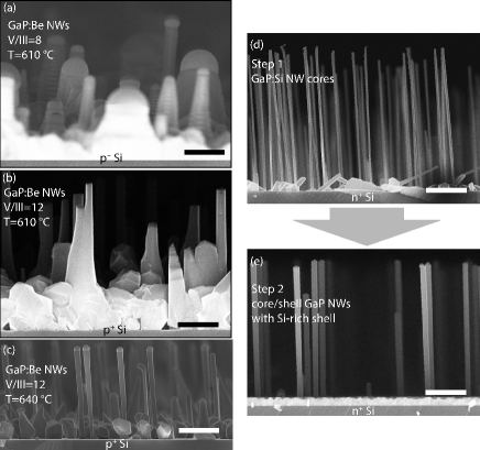
According to the previous reports on the growth of Be-doped GaAs NW, the question of beryllium incorporation efficiency via the nanowire side facets vapor-solid (VS) growth 17 or through the Ga droplet during the Ga-assisted VLS growth is debatable 18. However, it was shown, that regardless of the dopant incorporation path, strong lattice diffusion of Be enables homogeneous doping of NW 17. Our observations for the growth of GaP:Be NWs shows that at sufficiently high dopant fluxes Be accumulates in Ga droplet similarly to the case of GaAs:Be NWs reported in Ref. 18. In turn, Be-induced changes in the catalytic droplet morphology significantly narrow the growth window otherwise providing the uniform formation of vertical GaP NW (8 < V/III flux ratio < 30, 610 ∘C < Tgr < 630 ∘C) 19. It was found, that at high dopant fluxes Be tends to be accumulated in Ga droplet. Be-induced changes in the droplet morphology are clearly visible in Figure 1a,b showing SEM images of NW arrays grown under different V/III ratios. To study the catalytic droplet morphology, NW growth was interrupted by simultaneously closing P, Ga and Be fluxes. As a result, growth of GaP NW under Be flux at Tgr=610 ∘C and V/III=8 leads to the continuous Ga-droplet inflation suppressing axial NW growth and morphology changes visible on the NW side facet (see Figure 1a). On the other hand, as can be seen from Figure 1b, just 1.5-fold increase in the V/III flux ratio up to 12 leads to the absorption of the catalytic droplet interrupting VLS growth and coalescence of NWs at otherwise stable growth conditions. Thus, the range of V/III flux ratios allowing stable VLS growth turns out to be very limited, impeding the achievement of the optimal growth conditions. It was found that a stable VLS growth of GaP:Be NWs at the same Be flux can be achieved by an increase of the growth temperature Tgr up to 640 ∘C. SEM image of the Be-doped GaP NW array grown for 120 min at V/III=10 is shown in Figure 1c. The nanowires are 2.4 m long and 80-100 nm thick near the base and up to thickening to 150 10 nm near top facet, which is covered by catalytic droplet.
In contrast to the growth of Be-doped GaP NWs, introduction of maximal achievable Si flux available in our MBE-setup (TSi cell=1200 ∘C) does not lead to visible changes in the NW and catalytic droplet morphology. Our preliminary studies show that GaP:Si NWs demonstrate conductivity several orders of magnitude lower than expected, since the conductivity of single NW was below the sensitivity of our setup (10 pA). We associate such behaviour with amphoteric nature of silicon dopant and low probability of its incorporation on gallium sites, since self-catalytic VLS growth occurs in the excess of gallium 10. To avoid this limitation, we introduce a two-step growth technique allowing the efficient n-type doping of GaP NWs by Si, involving preliminary formation of a thin GaP:Si NW core in the self-catalytic VLS regime followed by the formation of a highly doped GaP:Si NW shell via the VS growth. Chosen Si flux corresponded to carrier concentration in the planar GaP layer of 7x1018 cm3. At the first step, the NW cores are grown under Si flux at Tgr of 630 ∘C and V/III fluxes ratio of 30 for 33 min. To stop the VLS growth, a catalytic Ga droplet is consumed keeping the of P2 and Si fluxes open for 20 min. As a result, a 3.80.8 m long and 6010 nm thick NW core is formed - see Figure 1d. At the second step, NW shell growth is carried out at reduced growth temperature of 500 ∘C and in excess of the group-V flux (V/III=40, which is roughly 7 times higher that stoichiometric flux ratio) for 60 min.
We suggest, that both low growth temperature and high value of group-V flux facilitate the incorporation of Si on Ga-sites contrasting to VLS growth under Ga-catalytic droplets. The obtained SEM image of the resulting GaP:Si core/shell NW array presented in Figure 1e confirms that radial growth prevails at the conditions chosen for the shell formation. The array possess relatively low surface density and high uniformity of NWs, which have the similar height of 4 m as the initial NW core and increased diameter of 160 and 130 ( 10) nm at the top and bottom facets.
For the further investigations, the doping type of Si-doped nanowires has to be defined. Si can be considered as amphoteric dopant for GaP, thus the doping type is ambiguous. It is known that silicon can give both n- or p-type conductivity in III-V NWs 20. In particular, in case of GaAs NWs, it’s shown that the doping type is governed by V/III flux ratio 20. In case of GaP NWs, Si behaviour as a dopant hasn’t been studied yet. To clarify the doping type of the grown NWs, we employed photo-assisted Kelvin Probe Force Microscopy measurements under in the presence of UV illumination. The technique description and the obtained results can be found in supplementary information. The results indicate that the nanowire surface potential rises under illumination meaning that the photovoltage is positive, and therefore, Si-doped GaP NWs possess n-type conductivity.
2.2 Conductive AFM study
The electrical conductivity of individual vertical NWs was investigated by obtaining their current-voltage characteristics (I-V curves). To do that, we used the nanopositioning technique based on conductive atomic force microscopy (C-AFM), which we have developed in several papers 21, 22, 23. First, we obtained the coordinates of several NWs by scanning the sample topography. Then we switched off the microscope feed-back system and manually positioned the grounded conductive probe tip to create mechanical contact with the NW top facet. Then we applied bias voltage to the conductive substrate and obtained the current signal in the substrate/NW/probe circuit as shown in Figure 2a. Taking into account relatively low surface density of the grown NWs, this approach excludes shunting the electric contact with neighbouring crystals. Figure 2b,c shows surface topography of both studied samples as well as the obtained I-V curves for several NWs. We present the data of 5 NWs for each sample, which coordinates are indicated on topographic images with blue wheel crosses. We analyze only the currents within 10 nA in order to exclude the nonlinear effects, induced by NW heating, appearing at higher currents.
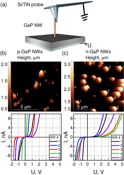
It can be seen that the obtained curves are rather smooth indicating stable tip-NW electrical contact during the measurements. Each acquired curve is well-reproducible which was proved by conducting several dozens of consistent measurements on the same NW. The curves were obtained in dark conditions (i.e. the sample is covered with an opaque dome and the AFM laser is switched off) to avoid the photogeneration in Si substrate. All measured curves show rectifying behaviour originating mainly from NW/tip Schottky and NW/substrate contacts. The curve shape varies significantly between several NWs of each sample. We associate this with the inhomogeneity of grown arrays. Thickness and doping level naturally varies from one NW to another within the same array. Also, the curve shape depends the top electric contact area which can be slightly different in each case 24.
2.3 Numerical modeling of I-V curves
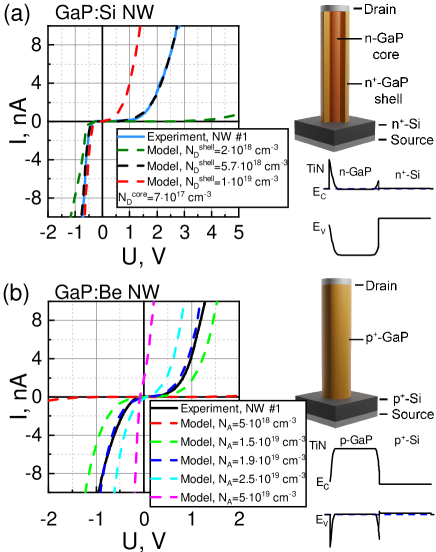
To estimate the NW doping level, numerical modeling of the obtained I-V curves was performed. It’s known that the curve shape is governed not only by NW intrinsic parameters such as doping concentration and carrier mobility, but also by contact and surface effects such as Schottky barrier height, contact area and surface depletion, which overall impact can change the curve shape from linear to rectifying 25. To distinguish the influence of different effects, we propose a 2D model in Silvaco Atlas software package. The NW parameters were estimated either from SEM (NW length and diameter) or from literature (GaP mobility and Schottky barrier height) and are listed in supplementary materials. We confine ourselves to modeling one curve for each sample, namely curves #1 from the figure 3, and vary the doping level and work function until the best fit is achieved, considering that all the remaining curves can be modeled as well with slightly different set of parameters. The best match for the chosen experimental curves was achieved with the following parameters: NDCore=71017 cm-3, NDShell=5.71018 cm-3, =1 eV. For GaP:Be NWs we have NA=1.91019 cm-3 and =1.15 eV. The full set of the used values is listed in supplementary information (see table S1).
The comparison of the modeled and experimental curves is presented in Figure 3. The doping level appears to be the most critical parameter, which variation within one order of magnitude completely modifies the NW electrical properties. At the same time, changing the NW geometry, mobility, and Schottky barrier within the accuracy of their estimation does not lead to such dramatic changes. Impact of the doping level on the I-V curve is explained by the balance of the Schottky- and hetero-barriers connected oppositely to the NW (see band diagram in Figure 3). The current in the circuit substrate/NW/probe depends on the tunneling current through the barriers, because the thermionic emission is low for the high energy barriers. Since the tunneling current dominates only at high doping level, reducing the doping dramatically decreases the current (see red curve in Fig. 3b).
2.4 I-V curves of horizontal GaP NW with lithographic contacts
C-AFM allows to study of the transport properties of numerous individual NWs which is helpful to gain statistical data and estimate their average doping level. However, the presence of Schottky barrier between the top NW facet and AFM probe complicates the analysis and can cause error. On the other hand, NW-based devices often consist of horizontally-dispersed NWs with Ohmic contacts from both sides. Thus, for validation of our numerical results and for the further development of horizontal geometry, we performed an additional independent experiment of a horizontal GaP:Si NW with two Ohmic contacts. To do that, the NW was transferred onto clean quartz substrate. After that, two metal electrodes were created using laser lithography. The creation of ohmic contacts to GaP is challenging due to the wide band gap and requires to use annealed contacts with an addition of doping metals. The main problem in case of NWs is that the annealing process can short the contacts together. To avoid this, we used the contacts based on activation process via solid phase diffusion under annealing. Based on the literature, the Pd/Si contact base is preferred to apply with NWs. The contacts were formed by depositing of Ni/Pd/Si/Al consistently with thicknesses of 3 nm, 15 nm, 30 nm, and 200 nm, respectively 26. The structure was annealed after metal deposition under different temperatures from 175 to 350 ∘C. The I-V curve obtained in such geometry is shown in Figure 4 from which it follows that 350 ∘C is sufficient annealing temperature for the contacts to become ohmic. SEM image of the NW is shown on the inset in Figure 4 which demonstrates no shorts between the contacts. Thus, the proposed approach is suitable for the formation of ohmic contacts to a single n-GaP NW, which is essential for NWs-based device development. To date, the formation of ohmic contacts to p-type GaP is still an issue, but we hope to implement and present it in future publications.

Then, specific differential resistance of the horizontal NW can be estimated as , where =1800 nm and =130 nm corresponds to the NW length and diameter respectively, and is a cross section area. Free charge carrier concentration is then calculated as cm-3 which is in good agreement with the value obtained in the previous section. Therefore, we believe that the proposed numerical model predicts the doping level with good accuracy. Taking into account uncertainties in determining , , , tip/NW contact area and Schottky barrier height, we can conclude that the achieved doping level lies in the range of ND=3-51018 cm-3 and NA=1-21019 cm-3 for GaP:Si and GaP:Be NWs respectively. Thus, the proposed growth strategies allow to synthesize samples which doping level is high enough for technological applications.
3 Conclusion
To conclude, in this work we synthesized bottom-up MBE-grown GaP NWs doped with Si and Be and investigated their electrical properties. We revealed a window of thermodynamic parameters facilitating a high rate of Be incorporation into GaP. We also introduced a core/shell growth algorithm allowing to use Si as an n-type dopant for GaP and successfully carried out the formation of ohmic contacts to a horizontal n-GaP NW. The I-V curves of individual NWs indicate the doping level on the order of ND=3-51018 cm-3 and NA=1-21019 cm-3 in case of GaP:Si and GaP:Be NWs respectively. The results open paths for the creation of axial and radial p-n junctions in GaP NWs facilitating their device implementation.
4 Acknowledgements
V.A.S acknowledges support of the electric measurements and numerical modeling by Russian Science foundation (Grant No. 23-72-01082). K.N.N. acknowledges support of the post-processing by Russian Science foundation (Grant No. 21-79-10346)
Conflicts of interest
There are no conflicts to declare.
Notes and references
- Barrigón et al. 2019 E. Barrigón, M. Heurlin, Z. Bi, B. Monemar and L. Samuelson, Chemical reviews, 2019, 119, 9170–9220.
- McIntyre and i Morral 2020 P. McIntyre and A. F. i Morral, Materials Today Nano, 2020, 9, 100058.
- Standing et al. 2015 A. Standing, S. Assali, L. Gao, M. A. Verheijen, D. Van Dam, Y. Cui, P. H. Notten, J. E. Haverkort and E. P. Bakkers, Nature communications, 2015, 6, 7824.
- Wilson et al. 2020 D. J. Wilson, K. Schneider, S. Hönl, M. Anderson, Y. Baumgartner, L. Czornomaz, T. J. Kippenberg and P. Seidler, Nature Photonics, 2020, 14, 57–62.
- Trofimov et al. 2020 P. Trofimov, A. P. Pushkarev, I. S. Sinev, V. V. Fedorov, S. Bruyère, A. Bolshakov, I. S. Mukhin and S. V. Makarov, ACS nano, 2020, 14, 8126–8134.
- Khmelevskaia et al. 2021 D. Khmelevskaia, D. Markina, V. Fedorov, G. Ermolaev, A. Arsenin, V. Volkov, A. Goltaev, Y. M. Zadiranov, I. Tzibizov, A. Pushkarev et al., Applied Physics Letters, 2021, 118, 201101.
- Sharov et al. 2022 V. A. Sharov, A. M. Mozharov, V. V. Fedorov, A. Bogdanov, P. A. Alekseev and I. S. Mukhin, Nano Letters, 2022, 22, 9523–9528.
- Kuznetsov et al. 2023 A. Kuznetsov, E. Moiseev, A. N. Abramov, N. Fominykh, V. A. Sharov, V. M. Kondratev, I. I. Shishkin, K. P. Kotlyar, D. A. Kirilenko, V. V. Fedorov et al., Small, 2023, 2301660.
- Kim et al. 2021 W. Kim, L. Güniat, A. Fontcuberta i Morral and V. Piazza, Applied Physics Reviews, 2021, 8, 011304.
- Dubrovskii et al. 2020 V. G. Dubrovskii, H. Hijazi, N. I. Goktas and R. R. LaPierre, The Journal of Physical Chemistry C, 2020, 124, 17299–17307.
- Diak et al. 2023 E. Diak, A. Thomas, V. G. Dubrovskii and R. R. LaPierre, Crystal Growth & Design, 2023, 5074–5082.
- Isik Goktas et al. 2020 N. Isik Goktas, A. Sokolovskii, V. G. Dubrovskii and R. R. LaPierre, Nano Letters, 2020, 20, 3344–3351.
- Dubrovskii and Hijazi 2020 V. G. Dubrovskii and H. Hijazi, physica status solidi (RRL) – Rapid Research Letters, 2020, 14, 2000129.
- Chen et al. 2010 Z.-G. Chen, L. Cheng, G. Q. M. Lu and J. Zou, Nanotechnology, 2010, 21, 375701.
- Yazdi et al. 2015 S. Yazdi, A. Berg, M. T. Borgström, T. Kasama, M. Beleggia, L. Samuelson and J. B. Wagner, Small, 2015, 11, 2687–2695.
- Hasenöhrl et al. 2013 S. Hasenöhrl, P. Eliáš, J. Šoltỳs, R. Stoklas, A. Dujavová-Laurenčíková and J. Novák, Applied surface science, 2013, 269, 72–76.
- Casadei et al. 2013 A. Casadei, P. Krogstrup, M. Heiss, J. A. Röhr, C. Colombo, T. Ruelle, S. Upadhyay, C. B. Sørensen, J. Nygård and A. Fontcuberta i Morral, Applied Physics Letters, 2013, 102, 013117.
- Zhang et al. 2018 Y. Zhang, Z. Sun, A. M. Sanchez, M. Ramsteiner, M. Aagesen, J. Wu, D. Kim, P. Jurczak, S. Huo, L. J. Lauhon and H. Liu, Nano Letters, 2018, 18, 81–87.
- Fedorov et al. 2021 V. V. Fedorov, Y. Berdnikov, N. V. Sibirev, A. D. Bolshakov, S. V. Fedina, G. A. Sapunov, L. N. Dvoretckaia, G. Cirlin, D. A. Kirilenko, M. Tchernycheva and I. S. Mukhin, Nanomaterials, 2021, 11, 1949.
- Hijazi et al. 2019 H. Hijazi, G. Monier, E. Gil, A. Trassoudaine, C. Bougerol, C. Leroux, D. Castellucci, C. Robert-Goumet, P. E. Hoggan, Y. André et al., Nano Letters, 2019, 19, 4498–4504.
- Alekseev et al. 2015 P. A. Alekseev, M. S. Dunaevskiy, V. P. Ulin, T. V. Lvova, D. O. Filatov, A. V. Nezhdanov, A. I. Mashin and V. L. Berkovits, Nano letters, 2015, 15, 63–68.
- Alekseev et al. 2019 P. A. Alekseev, V. A. Sharov, M. S. Dunaevskiy, D. A. Kirilenko, I. V. Ilkiv, R. R. Reznik, G. E. Cirlin and V. L. Berkovits, Nano letters, 2019, 19, 4463–4469.
- Alekseev et al. 2020 P. A. Alekseev, V. A. Sharov, B. R. Borodin, M. S. Dunaevskiy, R. R. Reznik and G. E. Cirlin, Micromachines, 2020, 11, 581.
- Lord et al. 2015 A. M. Lord, T. G. Maffeis, O. Kryvchenkova, R. J. Cobley, K. Kalna, D. M. Kepaptsoglou, Q. M. Ramasse, A. S. Walton, M. B. Ward, J. Köble et al., Nano Letters, 2015, 15, 4248–4254.
- Zhang et al. 2007 Z. Zhang, K. Yao, Y. Liu, C. Jin, X. Liang, Q. Chen and L.-M. Peng, Advanced functional materials, 2007, 17, 2478–2489.
- Park et al. 1997 M.-H. Park, L. Wang, D. Dufner, F. Deng, S. Lau, I. Tan and F. Kish, Journal of applied physics, 1997, 81, 3138–3142.