TOP: Towards Open & Predictable Heterogeneous SoCs
Abstract
Ensuring predictability in modern real-time Systems-on-Chip (SoCs) is an increasingly critical concern for many application domains such as automotive, robotics, and industrial automation. An effective approach involves the modeling and development of hardware components, such as interconnects and shared memory resources, to evaluate or enforce their deterministic behavior. Unfortunately, these IPs are often closed-source, and these studies are limited to the single modules that must later be integrated with third-party IPs in more complex SoCs, hindering the precision and scope of modeling and compromising the overall predictability. With the coming-of-age of open-source instruction set architectures (RISC-V) and hardware, major opportunities for changing this status quo are emerging. This study introduces an innovative methodology for modeling and analyzing State-of-the-Art (SoA) open-source SoCs for low-power cyber-physical systems. Our approach models and analyzes the entire set of open-source IPs within these SoCs and then provides a comprehensive analysis of the entire architecture. We validate this methodology on a sample heterogenous low-power RISC-V architecture through RTL simulation and FPGA implementation, minimizing pessimism in bounding the service time of transactions crossing the architecture between 28% and 1%, which is considerably lower when compared to similar SoA works.
1 Introduction
The exponential growth of cyber-physical systems (CPS) (e.g. self-driving cars, autonomous robots, …) and related applications has been fueled by the increase in computational capabilities of heterogeneous low-power Systems-on-Chip (SoCs). These SoCs are complex computing platforms composed of a set of different hardware computing units (e.g., CPUs, hardware accelerators), each tailored to a specific target application, sharing a set of resources (memory, sensors) through interconnects[1, 2, 3, 4].
While integrating multiple computing units on the same platform has enabled efficient scale-up of computational capabilities, it also poses significant challenges when it comes to assessing their timing predictability, which is a requirement for CPSs dealing with real-time and safety-critical applications: the primary challenge arises from resource contentions that emerge when multiple active agents within the SoC must access the same shared resources[1, 2, 5].
Numerous research efforts have focused on enhancing the predictability of heterogeneous Systems-on-Chip (SoCs). To do so, these efforts have predominantly focused on modeling and analyzing commercial DDR protocols [6], memory IPs [7] and memory controllers [8], but also predictable interconnects[2, 1] and on-chip communication protocols[9]. Regrettably, these modeling studies face substantial limitations regarding accuracy. Modeling and analysis of protocols are limited by construction: simulation and benchmarking are done speculatively on abstract models of the target system. At the same time, recent works for modeling and analysis of IPs (memories, memory controllers, interconnect, etc., …) have to address the unavailability of the cycle-accurate RTL descriptions of IPs: many of these IPs are either entirely closed-source[6] or provide loosely-timed behavioral models[8] or just architectural descriptions[2, 1, 10]. Furthermore, the fragmented and proprietary nature of commercial and research IPs restricts studies to a single IP at a time. These limitations greatly reduce the level of accuracy achievable through system-level analysis.
For example, Restuccia et al. in [11] bound the access times of multiple initiators on FPGA reading and writing from/to the shared DDR memory. The proposed upper bounds’ pessimism is between 50% and 90%: even though they finely modeled and analyzed the proprietary interconnect, the authors did not have access to its RTL nor to the memory controller and IP. The same applies to Ditty [12], which is a predictable cache coherence mechanism. In Ditty, even though the caches’ timing is finely modeled, the overall execution time can be up to 3 bigger than the theoretical upper bounds, as the authors did not model other components. Another example is [1], an advanced AXI interconnect with a sophisticated scheduler which allows transaction prioritization based on importance. While proposing a highly advanced interconnect with a tightly coupled model, the authors do not extend the model to the other components of the SoC, even when assessing the deadline miss ratio and benchmarking the architecture.
The emergence of open-source hardware creates a major opportunity for building accurate end-to-end models for real-time analysis of cutting-edge heterogeneous low-power SoCs [13, 14, 4]: the openness of the IPs allows for cycle-accurate analysis of the whole architecture from the interconnects to the shared resources. Yet, investigations and successful demonstrations in this direction are still scarce, mostly due to the fact that open hardware has only very recently reached the maturity and completeness levels required to build full heterogeneous SoCs[15].
In this work, we leverage a set of open-source IPs, which belong to the PULP family (one of the most popular open-hardware platforms proposed by the research community [13, 16]), and present an in-depth architectural analysis and a novel methodology to model and analyze heterogeneous SoC architectures, with the main aim of supporting timing predictability in safety-critical applications and providing safe upper bounds for the access times within the architecture. The contributions of this work are the following: (i) a novel fine-grained model for the typical resources composing a modern SoC; (ii) a fine-grained analysis of all the components of an SoC, directly based on their RTL, and (iii) a full system-level mathematical analysis to upper bound the response time of the interactions between managers (initiators) and shared subordinates (targets), considering the maximum interference generated by the interfering managers. The target architecture is a prototype of a State-of-the-Art (SoA) open-source SoC for embedded systems, composed of a Linux-capable host core coupled with a parallel accelerator, a set of IOs, and on-chip and off-chip memories, managed by a lightweight DDR controller[4, 14]. We leverage the availability of the codebase of the platform under analysis and propose a holistic approach. Our analysis covers the whole hardware architecture in detail, limiting the proposed upper bounds’ pessimism, which ranges between 28% and just 1%, in isolation and under interference. This is considerably lower when compared to similar SoA works for closed-source platforms[3, 12, 1, 10, 2, 6], as detailed in Section 7.
The manuscript is organized as follows: Section 2 presents the open-source RISC-V-based SoC architecture we target with our analysis, and Section 3 discusses the model we apply to the different components of the architecture. Section 4 analyzes the components to specialize the generic model to each of them, and Section 5 provides the system-level analysis of the architecture. Finally, Section 6 validates the results with cycle-accurate experiments (on simulation and FPGA), and Section 7 compares this work with the SoA. Section 8 concludes the manuscript.
2 Architecture
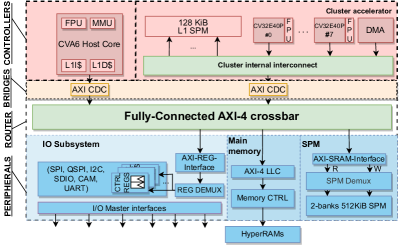
Fig. 1 shows the architectural template we target. It also shows the four classes of hardware modules we identify in the architecture under analysis, namely (i) controllers, (ii) the main crossbar, (iii) bridges, and (iv) peripherals, which we model in the next Section. The architecture leverages a set of fully open-source PULP IPs[16]. It is based on Cheshire[14], an open-source host platform consisting of an RV64 Linux-capable CPU, a set of commodity IOs (SPI, SDIO, UART, …), and an AXI-based crossbar with a configurable number of subordinate and manager ports for easy integration of accelerators and resources. Connected to the crossbar, our platform includes a parallel accelerator and a low-power lightweight HyperBUS memory controller[17].
The host CPU is CVA6[18], which is a 6 stages, single-issue, in-order, 64-bit Linux-capable RISC-V core, supporting the RV64GC ISA variant, SV39 virtual memory with a dedicated Memory Management Unit (MMU), three levels of privilege (Machine, Supervisor, User), and PMP [19]. The parallel hardware accelerator is the so-called PULP cluster[20]. It is built around 8 CV32E4-based cores [21] sharing 168 kB SRAM banks, composing a 128 kB L1 SPM. Each core has a private Floating Point Unit (FPU) supporting single-precision (FP32) and half-precision (FP16) floating-point formats. The cluster also features a hierarchical I-cache directly connected to the cluster’s internal AXI interconnect.
CVA6 and the cluster are the managers of the systems connected to the main AXI crossbar[22], which routes their requests to the desired subordinates according to the memory map. The main subordinates of the systems are, respectively (i) the on-chip SRAM memory, (ii) the APB subsystem, and (iii) the off-chip main memory. The on-chip memory is used for low-latency, high-bandwidth data storage. The APB subsystem is used to communicate with off-chip sensors or memories through the commodity IOs. Differently from high-end embedded systems relying on relatively power-hungry and expensive DDR3/4/5 memories, the platform under analysis adopts HyperRAMs as off-chip main memory, which are fully-digital low-power small-area DRAMs with less than 14 IO pins and that provide enough capacity to boot Linux [4] and bandwidth for IoT applications[23, 17].
3 Model
This section presents the model we construct for the different components of our SoC. Our aim is to propose a general model and analysis that can be re-targeted to possible modifications of the platform under analysis and/or novel architectures. In this regard, this work is also an effort to provide base support to stimulate the research community in the direction of further studies in predictability improvements and analysis for open hardware architectures.
3.1 Communication model
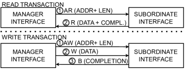
As mentioned in the previous Section, we identify four classes of hardware modules in the architecture under analysis, shown in Fig. 1, namely (i) controllers, (ii) the main crossbar, (iii) bridges, and (iv) peripherals, which we model in this Section. The AXI standard is the main communication standard used to implement on-chip communications. It defines a manager-subordinate interface enabling simultaneous, bi-directional data exchange and the ability to issue multiple outstanding transactions. Fig. 2 shows the AXI channel architecture and information flow. Bus transactions are initiated by a controller (exporting a manager interface), submitting a transaction request to read/write data to/from a subordinate interface through AR or AW channels, respectively. A request describes the starting target address and a burst length. After the request phase, in case of a read, data are transmitted back through the R channel. In case of a write, data are provided by the controller to the target peripheral through the W channel. Upon completing a write transaction, the peripheral also sends a beat on the B channel to acknowledge the transaction’s completion. Data channels depend on address channels. When there are multiple in-flight transactions, for writes, the standard enforces strict in-order access to the W channel – the data on the W channel must be propagated in the same order as the requests have been propagated on the AW channel. Even though the standard does not require such in-order enforcement on multiple in-flight read transactions, many commercial and open-source platforms feature an in-order implementation choice also on reads, typically to limit the overall complexity of the system, as also reported in their documentation [24, 25, 26].
3.2 Controller model
Controllers have an active role on the bus. Each controller exports an AXI manager interface, through which it initiates requests for bus transactions directed to the peripherals. A generic controller can be described through two parameters: the maximum number of outstanding read/write transactions that it can issue in parallel, denoted with , and their relative burst length . While our model and analysis can be applied to a generic architecture, the system under analysis features as controllers a CVA6 core [18] and a cluster accelerator [20] (see Section 2). CVA6 is assumed to compute a critical periodic workload, running on top of a Real-time Operative System (RTOS), which must be conscious of the maximum response times of such bus transactions to properly schedule the tasks without incurring deadline misses. The cluster accelerator is autonomous in making read/write transactions to the shared resources – the internal DMA generates bus transactions for data fetching and writing output results. Bus transactions issued by the cluster interfere with the transactions issued by the CVA6, and vice-versa – our analysis focuses on the upper bound of the maximum temporal interference to support the safe execution of critical tasks on either the CVA6 and the cluster, i.e., that critical tasks are executed within their deadline.
3.3 Peripheral model
Peripherals export a subordinate interface, through which they receive and serve the bus transactions issued by controllers. The peripherals deployed in the system are heterogeneous. However, they share common behaviour from the point of view of a worst-case timing analysis. This section provides a model for a generic peripheral – we leverage this as the baseline to provide a custom-specific analysis for any peripheral deployed in the system under analysis (see Section 4). The generic peripheral is characterized with two sets of parameters: (i) the maximum number of supported outstanding reads () and write () transactions, i.e., the maximum amount of pending transactions concurrently accepted by the peripheral for read and write, respectively; (ii) the worst-case service time in isolation for a read () and a write () transaction, defined as the maximum number of cycles incurred from the reception of the request to its completion for read and write transactions, respectively. and are composed of two contributions: (i) the data time , defined as the time required for the peripheral to send or receive one word of data () multiplied by the burst length of the transaction in service () and (ii) the control overhead , defined as the maximum time elapsing between receiving of the request and the availability of the first word of data (read transactions) or the availability to receive data (write transactions). From the previous considerations, . We define two extra parameters and . The first indicates the level of pipelining in serving multiple transactions. means that each pipeline stage of does not stall the previous stages, and transactions are served in a pipelined fashion, while indicates that no pipeline is implemented. indicates that read and write transactions interfere with each other within the peripheral. indicates that read and write transactions can be handled in parallel by . This is further described in Section 5.
3.4 Main crossbar model
In the architecture under analysis, the fully connected AXI-4 crossbar (also referred to as crossbar) is the routing component enabling communication among controllers and peripherals happening. Each controller has its manager port connected to a subordinate port of the crossbar. Dually, each peripheral has its subordinate port connected to a manager port of the crossbar. The crossbar has a crucial role in defining the performance and parallelism of the platform. We model the crossbar with two sets of parameters able to capture both of such effects: (i) the maximum number of outstanding transactions allowed for each controller, defined as the maximum amount of pending transactions allowed from a generic controller connected to for read transactions () and write transactions (); and (ii) the maximum overall latency introduced by on each read transaction () and write transaction (). and are composed of two contributions: (i) the propagation time (), defined as the overall delay introduced by the crossbar on a whole transaction when no contention is happening; (ii) the maximum arbitration latency defined as the maximum time a request is delayed at the arbitration stage due to the contention generated by other interfering transactions. From the previous considerations, the propagation latency is modeled as . Such parameters directly depend on the arbitration policies and routing mechanisms, as we investigate in detail in Section 4.
3.5 Bridge model
Bridges export a single manager interface and a single subordinate interface. They serve as an exclusive link for protocol/clock conversion between a controller and the crossbar – no contention can be generated at the bridge level. Bridges require a certain number of clock cycles to be crossed by a transaction but do not limit the number of in-flight transactions that can be issued. Thus, we model the bridges with two parameters: the overall maximum propagation latency for (a) read () and (b) write () transactions, defined as the delay introduced over a whole transaction.
4 Analysis of the hardware modules
This section aims to analyze the worst-case behavior of the peripherals, bridges, and the crossbar present in the platform under analysis. Our approach is compositional – in this Section, we analyze each hardware component separately, specializing in the generic models introduced in Section 3, and bounding the service times at the IP level in isolation. In the next Section, we provide an overall worst-case analysis at the system level, in isolation and under interference. To keep our analysis general, we assume that any component under analysis has its own clock so that, for instance, is the clock of the SPM memory.
4.1 AXI CDC FIFO queues
AXI CDC FIFOs are leveraged to perform clock-domain crossing between two AXI-based devices. The generic AXI CDC FIFO is a bridge: we apply here the model presented in Section 3.5. It exports a manager interface and a subordinate interface. It is composed of five independent CDC FIFOs, each serving as a buffer for an AXI channel, having depth (design parameter for the IP under analysis).
4.1.1 RTL IP structure
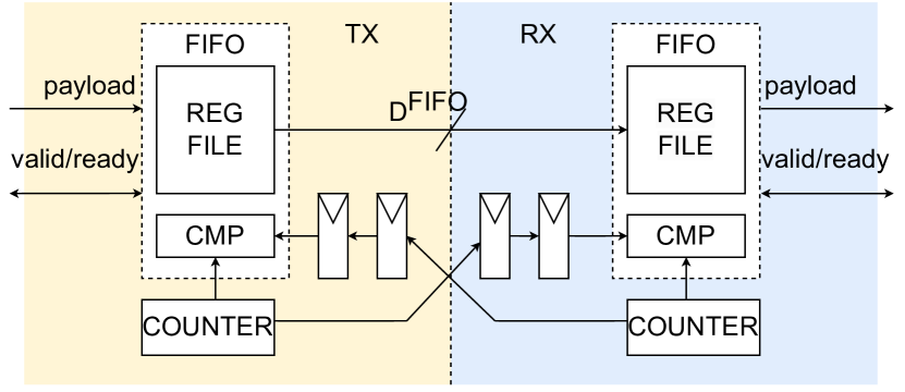
Figure 5 shows the block diagram of a CDC FIFO in the platform under analysis. They are structured following established clock domain crossing (CDC) principles [22]. The design is split into two parts, the transmitter (TX) and the receiver (RX), having different clock domains. TX and RX interface through asynchronous signals, namely a counter for data synchronization (synchronized with two-stage Flip-Flops (FFs)) and the payload data signal.
4.1.2 Delays analysis
As mentioned earlier, CDC FIFOs are bridges. Thus, we apply the model presented in Section 3.5. Considering the propagation delays, for each channel, the CDC FIFO under analysis behaves as follows: TX samples the payload data into an FF. In the following cycle, the TX counter is updated. The TX counter value gets then through two synchronizations FFs – the updated pointer value is observed by the RX after two clock cycles. At that point, RX samples the data in one clock cycle to then propagate it in the following one. From the previous considerations, crossing the CDC FIFO introduces a fixed delay of one clock cycle of the TX domain () and four clock cycles of the RX domain (). This means that the delay in crossing once the CDC FIFO is equal to . Following, we leverage this baseline delay to build the overall delay introduced by on read and write transactions.
Read transaction: assume that is interposed between a manager side (clocked at ) and a subordinate side (clocked at ). A read transaction (generated at the manager side) crosses . According to the AXI standard [27], is composed of two phases: (i) the address propagation phase and (ii) the data phase. This means that the CDC FIFO is crossed twice to complete : during phase (i) the manager is on the TX side, propagating the request. In phase (ii), the subordinate is on the TX side, propagating the data. From the previous considerations and applying now the baseline equation previously introduced, the propagation latency is in phase (i) and in phase (ii). Adding them together, the overall propagation latency introduced by on is equal to:
| (1) |
Write transaction: similar considerations can be applied to a generic write transaction crossing . A write transaction is composed of three phases: (i) an address phase (manager on the TX side), (ii) a data phase (manager on the TX side), and (iii) a write response phase (subordinate on the TX side). The request and the corresponding write data are propagated in parallel (as from the definition of the AXI standard, see [27] p. 45). Thus, is incurred for phases (i) and (ii). Then, a delay of is incurred to propagate the write response. From the previous considerations, the delay introduced by on has the same contributions as the delay introduced in Equation 1, .
4.2 AXI SRAM scratchpad memory (SPM)
The AXI scratchpad memory (SPM) is a high-speed, low-latency memory component used for temporary data storage – a block design representation is reported in Figure 5. The SPM memory is a peripheral – thus, we apply here the model presented in Section 3.3.
4.2.1 RTL IP structure
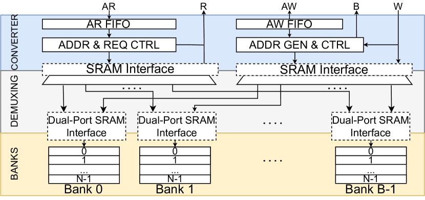
The first stage of the SPM architecture is represented by a protocol converter (AXI-SRAM-Interface), which translates the two read and write AXI channels into SRAM-compatible transactions. Following the converter, an internal demux directs the SRAM transactions to the desired target SRAM bank, in which the data is stored. Each SRAM bank provides two SRAM ports, one for reads and one for writes. Following the specification from industry-standard SRAM resources [28], the two channels are independent.
The AXI-SRAM-Interface is structured in two submodules, independently managing read and write transactions, respectively. Each submodule outputs a SRAM-compatible port. The first stage of each submodule is a FIFO queue (of depth ) buffering the AXI AW or AR channel, respectively. Each submodule features the logic for protocol translation, consisting of (i) saving transaction metadata (starting address and length) and (ii) producing the output SRAM requests. The incoming data on the W channel are directly propagated towards the banks. The logic operating the protocol conversion is in charge of generating the address for each W beat. Also, the data coming from the SRAM banks are directly driven on the R channel. The logic keeps compliance with the AXI standard, adding the last signal or generating write responses when required. The demux is fully combinatorial – the target bank is selected according to the address of the request. The SRAM banks are technology-specific macros instantiated at design time. Each SRAM bank’s port exports an enable signal, an address signal, and a flag signal, determining if a transaction is a read or a write. The SRAM interface expects simultaneous propagation of data and commands for write transactions; for read, the requested data are sent the cycle following the command.
4.2.2 Delays and parallelism analysis
AXI-SRAM-Interface: the FIFOs in the converter are only in charge of data buffering – each FIFO introduces a fixed delay of one clock cycle () (differently from the CDC FIFOs introduced in Section 4.1). After the FIFOs, the control logic requires at most one clock cycle to set up the propagation of a burst transaction – the direct connection over the W and R channels makes the data streaming in a pipeline fashion, adding no further latency. At the end of a write transaction, the converter takes two clock cycles to generate the write response: in the first clock cycle, it acknowledges that the last W beat has been accepted. In the following, it provides the B response. The same applies for reads, to correctly generate the AXI last signal. As mentioned earlier, after the initial protocol conversion, the transactions on the R and W channels are directly merged with SRAM transactions. Summing up the contributions, the control latency introduced by the AXI-SRAM-Interface to each transaction is upper bound by for both reads and writes.
Demux: The demultiplexing of the transaction is fully combinatorial and it directly connects the transaction to the SRAM bank – by design, it is guaranteed to execute within one clock cycle ().
Banks: As by the definition of the SRAM interface [28], an SRAM bank serves one transaction per clock cycle, which makes . For write transactions, it is guaranteed by the protocol that the SRAM bank samples the data in parallel with the request (in the same clock cycle). In read transactions, the delay in serving data is of one clock cycle, i.e., the data are served the exact clock cycle after the bank samples the request. So, it contributes to with one additional clock cycle (). Summing up the contributions, the maximum service time of the SPM in isolation is upper bound by:
| (2) |
Consider now the parallelism supported by the SPM. The maximum number of accepted outstanding transactions at the SPM is defined by the depth of the input buffers implemented in the AXI-SRAM-Interface. Thus,
| (3) |
The SPM module under analysis is aggressively pipelined, operations are guaranteed to be executed in one clock cycle, and no stall sources are present in the design. Also, as mentioned earlier, read and write transactions can be handled in parallel without any interference. From the previous considerations, and .
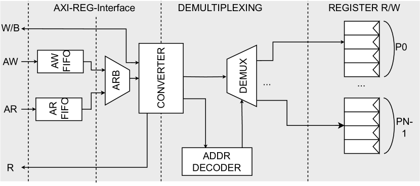
4.3 IO Subsystem
The IO subsystem is the peripheral in charge of writing/reading data to/from the off-chip I/Os. We apply here the model presented in Section 3.3. It is composed of a set of memory-mapped peripheral registers accessed through a demux. Each I/O interface (e.g., SPI, I2C, …) has its private set of memory-mapped registers, written or read by a controller (in our case, the CVA6), managing the datapath which actually issues the transactions on the buses.
4.3.1 RTL IP structure
Figure 5 shows the block diagram of the IO subsystem – this is composed of an AXI-REG-Interface, a demux, and a set of registers. As in the AXI-SRAM-Interface, the first stage of the AXI-REG-Interface is composed of two FIFOs for data buffering (of depth ) – one for read transactions, one for write transactions. Within the interface, a round-robin arbiter arbitrates the access of read and write transactions and lets through only one at a time to the actual protocol conversion logic, deployed after the FIFOs. Registers’ transactions share the same set of signals for reads and write and are limited to single-word accesses. Differently from the AXI SPM, the IO subsystem is meant for low-power reads and writes. For such a reason, the IO subsystem in the platform under analysis does not support burst transactions (requests having are suppressed). Such a feature simplifies the control logic. The demux stage is in charge of decoding the request and directing it to the proper register destination, where it is finally served as a register read or write.
4.3.2 Delays and parallelism analysis
The IO subsystem is a peripheral, thus, we apply the model proposed in Section 3.5. Considering the maximum service delays, overall, the IO subsystem is composed of four pipeline stages: (i) the FIFOs, (ii) the protocol conversion, (iii) demultiplexing, and (iv) target register access. The first three stages, contributing to the control overhead, are guaranteed by design to introduce a fixed delay of one clock cycle () each for a total of clock cycles. Considering stage (iv), registers are guaranteed by design to provide (read) or store (write) data in one clock cycle. In the case of a write, the protocol dictates that the request and the corresponding data are propagated in parallel in one clock cycle. In the case of a read, the register provides the data in the clock cycle following the request – requires one extra clock cycle. Summing up all the contributions, the delays introduced by the I/O subsystem are upper bounded by:
| (4) |
Consider now the parallelism of the IO subsystem. Similarly to the SPM module, the IO subsystem is capable of buffering up to of each type in its input FIFO queues deployed in the AXI-REG-interface. Thus, the maximum number of outstanding transactions supported by the IO subsystem is equal to:
| (5) |
However, differently from the SPM, the IO subsystem serves read and write transactions one at a time, and no pipelining is implemented among the different stages. This means that and .
4.4 The main memory subsystem
As for the rest of the system, the main memory subsystem is entirely composed of open-source IPs. The availability of its RTL allowed us to provide a detailed analysis, which is quite unique for a whole complex memory subsystem. It is a peripheral – thus, we apply here the model presented in Section 3.3. It is composed of three macro submodules: (i) the AXI Last-level Cache (LLC); (ii) the HyperRAM memory controller (HMC); and (iii) the HyperRAM memory (HRAM). It is based on HyperRAM memories leveraging the HyperBUS protocol [23]. HyperRAMs are optimized for low-overhead data storage while offering up to 3.2Gbps bandwidth. To keep a low pin count, HyperRAMs expose a fully digital 8-bit double-data-rate (DDR) interface to be used both for commands and data. The HyperRAMs serve transactions in order, one at a time, as required by the protocol [23]. While a pure in-order strategy is simplified with respect to the ones deployed by high-end commercial memory controllers, it is worth mentioning that these are generally complex closed-source IPs difficult to model and analyze. Nevertheless, while essential, the memory subsystem under analysis has demonstrated to be effective in tape-outs of Linux-capable chips [4].
4.4.1 RTL IP structure

The AXI Last-Level Cache is the interface of the memory subsystem with the platform. The LLC under analysis has configurable cache line length, defined as . Figure 6(a) shows the LLC’s block diagram, composed of 5 pipelined units: (i) burst splitter, (ii) hit-miss detection, (iii) eviction/refill, (iv) data read/write, and (v) data ways. Figure 6(b) shows how these units cooperate to serve the incoming requests. The burst splitter is in charge of buffering and splitting the incoming AXI requests into multiple sub-requests having the same length of the cache line () and of calculating and appending the tags of the transactions. A -word AXI burst request is split internally into requests of length . The tags are the input to the hit-miss detection unit, which analyzes them to determine if any sub-request will be a (a) hit or (b) miss. In case (a), the transaction is directed to the read/write unit: if it is a (a.i) read, the read response is generated and immediately sent through the AXI subordinate port, and the transaction is completed. In the case of a (a.ii) write, the locally cached value is updated and a write response is generated and sent back on the AXI interface to complete the transaction. In case (b), the transaction is submitted to the eviction/refill unit. Refill consists in issuing a read to the memory controller to get the missing data to then update the data way. Eviction consists in freeing a spot in the local cache. A Least Recently Used (LRU) algorithm is used in the module under analysis. Refills are performed on every miss, both for read and write transactions. Evictions are performed only when a cache set is full, before a refill, to free the necessary spot.
The HyperRAM memory controller [29] is depicted in Figure 6(c). It consists of two tightly coupled modules working in two separated frequency domains: (i) the AXI front-end and (ii) the back-end PHY controller. The front-end handles and converts the AXI transactions into data packets for the PHY controller, and it runs at the same clock as the LLC (). The back-end features a lightweight Finite State Machine (FSM) to send/receive the data packets, keeping compliance with the HyperBUS protocol timings and data flow and it runs at the same clock as the HyperRAMs (). The back-end handles two off-chip HyperRAMs in parallel, configured with interleaved addresses. Each HyperRAM arranges data as 16-bit words. Thus, overall, the word size of the back-end is bits.
The first stage of the front-end is composed of two FIFOs buffering incoming AXI read and write requests. The FIFOs are connected to a serializer, solving conflicts among reads and writes in accessing the AXTOPHY converter and letting through one transaction at a time. Following, three modules translate between AXI and the back-end protocol: (i) AXTOPHY, translating the AXI AW or AR requests into commands for the back-end; (ii) PHYTOR converting the data words provided by the back-end into AXI read beats to be provided to the AXI interface; and (iii) WTOPHY, converting AXI W data beats into data words and generating write response at the end of the transaction. Since the front-end and back-end reside in two different clock domains, three CDC FIFOs are deployed between the frontend’s AXTOPHY, WTOPHY, and PHYTOR and the back-end. The back-end deploys an internal FSM arranging the requests coming from the front-end into 48-bit vector requests, as required in the HyperBUS protocol, and propagating the data packets to/from the two physical HyperRAM memories through two transceivers (TRX).
The HyperRAM memory is an off-chip memory IP [23]. It is provided with a cycle-accurate model (verification IP), fundamental for our analysis purposes [30]. Each HyperRAM is organized as an array of 16-bit words and supports one outstanding burst transaction. Each HyperRAM supports up to 1kB long burst. As two HyperRAM are interleaved, the overall burst can be up to 2kB long[17].
4.4.2 Delays and parallelism analysis
We now bound the worst-case service time of the main memory subsystem, analyzing its components one at a time. Starting with the LLC, we follow the control flow diagram reported in Figure 6(b) to guide the explanation. When an incoming request arrives at the main memory, either a read or a write, it is collected at first by the LLC – three scenarios can happen: (i) LLC cache hit, (ii) LLC cache miss with refill, and (iii) LLC cache miss with eviction and refill.
In case (i), the request is directly managed by the LLC – no commands are submitted to the HMC. The request proceeds through the LLC splitter, hit/miss unit, read/write unit, and data way stages. By design, each stage of the LLC requires a fixed number of clock cycles to perform its operation. The burst splitter executes in one clock cycle (). The hit/miss detection stage takes two clock cycles () – one for tag checking and one to propagate the request either to the read/write unit or the evict/refill unit. The read/write unit requires two clock cycles (), one to route the transaction to the data way, one to prepare the read data or write response beats back to the AXI input interface. The data ways, accessed by the read/write unit, are implemented with SRAM macros (same macros as the SPM, Section 4.2): after the propagation of the request, requiring one clock cycle (), the SRAMs take one clock cycle to provide the read data (). No further latency is required on writes as data is accepted together with the request. The read/write unit is also in charge of generating the write response at the end of the write transaction, which takes an extra clock cycle (). This means that either in the case of read or write, the data ways take two clock cycles (). Summing up the contributions, the main memory subsystem service time in case of a hit is upper bound by:
| (6) |
Consider now case (ii) and (iii). In these cases, also the eviction and refill stage is involved at the LLC level, and a read (for refill) and, optionally, a write (for eviction) is issued to the main memory. The eviction/refill stage operates eviction and refill operations in parallel. Eviction and refill consist of two operations each: (a) generating a transaction for the main memory; (b) generating a transaction for the data way. Each of such operations takes one clock cycle. Thus, the overall delay contribution of this stage is . Hence, the LLC control time in case of a miss is upper bounded by:
| (7) |
Consider now the delay introduced by the HyperRAM memory controller on a generic request. Later, we will use this delay to bound the service time on the batch of transactions issued by the LLC. On each transaction, the HMC contributes to the worst-case service delay with the sum of the worst-case delay latency introduced by (a) the front-end, (b) the back-end, and (c) the CDC FIFOs between them. Consider (a): each one of the front-end’s submodules takes one clock cycle to sample and process the incoming transaction, except for the serializer, which takes two. Read and write transactions pass through 4 modules (FIFOs, serializer, AXITOPHY and either WTOPHY or PHYTOR): this makes the overall delay contribution of the front-end equal to . Consider now the CDC FIFOs – these are the same as the one composing the AXI CDC FIFOs introduced in Section 4.1. The CDC contributes differently to reads and writes. For writes, the CDC FIFO between the AXTOPHY and the back-end and the CDC FIFO between WTOPHY and the back-end propagate transactions from the front-end, transmitting the request and data – these two phases happen in parallel. Considering the results reported in Section 4.1, the delay introduced by the CDC on a write transaction is upper bound by . For reads, the transmitter is once the front-end (propagate the request from AXTOPHY) and once the back-end (propagate back the data to PHY2R) – the delay introduced by the CDC on a read is upper bound by . Lastly, consider (c) the HMC back-end. The back-end’s FSM parses the incoming request into a HyperRAM command in one cycle (). Following this, an extra cycle is required for the data to cross the back-end. Summing up the contributions just described, the control time of the HMC on a generic transaction is upper bound by:
| (8) |
Consider now the delays introduced by the HyperRAM memories on a generic request. The control overhead time to access the HyperRAM memory is defined by the HyperBUS protocol [23]. As the first step, the 48-bit HyperRAM command vector is sent over the two memories. As the HyperBUS command bus is 16 bits, the command vector propagation takes clock cycles. Following, the HyperBUS provides a fixed latency for the maximum time to access the first data word, accounting for refresh effects and crossing row boundaries – the specifications [31] bound such a delay between 7 and 16 clock cycles. In our case, this is set to . Thus, the total control latency of the HyperRAM memory is upper bound by:
| (9) |
At this point, data are ready to be propagated. As the AXI domain and the HyperRAM might have different domain size, the number of cycles to send/receive an AXI word is:
| (10) |
We now have all the elements to bound the overall service time of the whole main memory subsystem in case of a miss (ii) with refill and (iii) eviction and refill. First, we bound the service time of the memory controller and the memories to serve a refill request issued by the LLC, i.e., case (ii): given the splitting performed by the LLC, a -long transaction is split into sub-transactions, each -long. According to the standard [31] and our analysis, the transactions are served one at a time by the memory controller and the memory. To bound the control time on the batch of transactions, we multiply the upper bound of the control time of each sub-transaction by the number of transactions issued , and sum it with the control time of the LLC in case of a miss (). The same reasoning applies to the data time: due to the splitting, the total number of values requested by the LLC to the memory will be equal to , and not . This makes the overall time spent reading and, therefore, the data time for each word of the words equal to . To this data time, we add the data time of the LLC () and obtain the upper bound for the data time in case (ii). Thus, for case (ii), control and data time are bound as follows:
| (11) |
If the eviction is also required, i.e., case (iii), extra write transactions of length must be performed to save the evicted data to the HyperRAM. Following the same reasoning as earlier, the upper bounds for the overall control and data times on this batch of transactions are respectively and . To upper bound the overall control and data time, we sum these numbers to the service times of case (ii) and obtain the following:
| (12) |
Consider now the parallelism of the main memory subsystem. This is defined by the LLC, which acts as interface with the rest of the platform. In the platform under analysis, the LLC input buffers support up to read and write transactions. This mean that the maximum number of supported outstanding transactions is as follows:
| (13) |
The LLC is pipelined: in the case all the enqueued accesses are hits, there is no stalling, similarly to the SPM. However, the memory controller handles only one outstanding transaction at a time, stalls the preceding ones, and only serves one read or one write at a time. hence, as soon as one access is a miss, and .
4.5 AXI host crossbar
The AXI host crossbar deployed in the platform under analysis is a consolidated AXI crossbar already deployed and validated on multiple silicon tapeouts [4],[14], [22]. We apply here the generic model for the crossbar proposed in Section 3.4. The crossbar is referred as .
4.5.1 RTL IP structure
as detailed in Figure 7, the crossbar exports a set of input subordinate ports (S) and output manager ports (M). Each S port is connected to a demultiplexer, in charge of routing incoming AW and AR requests and W data to the proper M destination. Each M port is connected to a multiplexer, in charge of (i) arbitrating conflicting AW and AR requests directed to the same peripheral through a round-robin scheme, (ii) connecting the W channel of the one controller with access to the peripheral, and (iii) routing back the R read data and B write responses to the proper destination, according to the ID field. In general, the crossbar under analysis can be configured for a fully combinatorial (i.e., performing decoding and routing operations in a single clock cycle) or pipelined structure featuring up to three pipeline stages. In the platform under analysis, it is configured to be fully combinatorial.
4.5.2 Delays and parallelism analysis
Analyzing the maximum propagation delays introduced by the crossbar, we upper bound the overall latency on a transaction, combining the delays on each channel considering the structure of AXI reads and writes. It is worth mentioning that, differently from the other analyzed components, the maximum delays introduced at the crossbar level depend on the interference generated by the other controllers. For such a reason, we provide two upper bounds, one for transactions in isolation (which coincides with as defined in Section 3) and the other for transactions under contention (which coincides with as defined in Section 3). We will use both of them in our architectural analysis reported in Section 5.
Maximum delays in isolation: The crossbar is configured as a combinatorial structure. Thus, it is guaranteed by design that a request for a transaction, a data word, or a write response crosses the crossbar in one clock cycle (). Consider a whole AXI transaction. An AXI read transaction is composed of two phases involving the AR and R AXI channels – for each read transaction, the crossbar is crossed twice. Write transactions, instead, are composed of three phases involving the AW, W, and B AXI channels. For each AXI write transaction, the crossbar is crossed two times: the first time is crossed by the AW and W beats (propagated in parallel), and the second time by the B response. To complete either a read or write operation, the crossbar is crossed twice. Thus, the propagation delays in isolation is equal to:
| (14) |
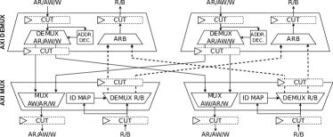
Maximum delays under contention: Under contention, multiple controllers connected to the crossbar can attempt to concurrently access the same peripheral, generating interference at the multiplexer arbitrating AR and AW requests accessing the peripheral. In the crossbar under analysis, the arbiters deploy a round-robin scheme capable of granting a request for each clock cycle. In the worst-case scenario, each interfering controller concurrently attempts to propagate a request to the same peripheral – in either read and write cases, the request under analysis loses the round-robin cycle and is served last, experiencing a delay of clock cycles (with the number of controller capable of interfering with the request under analysis). From the previous considerations, the maximum propagation time experienced by either a read or write transaction at the crossbar is upper bound by:
| (15) |
Consider now the parallelism. As far as read transactions are concerned, incoming read requests are propagated by the crossbar without any limitation on the maximum number of outstanding transactions: it leverages the AXI ID to route the transactions. The behavior is different for writes: AXI enforces a strict in-order execution ordering on write transactions (see page 98 of AXI specifications [27]). This requires the crossbar to implement a table to keep track of the order of granted transactions – the maximum number of outstanding write transactions per S port is limited by the depth of such tables, refereed as . From the previous consideration: . In the architecture under analysis, is set to be bigger than the parallelism supported by the peripherals within the SoC to prevent the crossbar from limiting the overall parallelism of the system.
5 System-level worst-case response time analysis
This section introduces our system-level end-to-end approach to upper bound the overall response times of read and write transactions issued by a generic controller and directed to a generic peripheral, considering the maximum interference generated by the other controllers in the system. Our approach is static[32] and compositional[33]. Specifically, we leverage the component-level static analysis introduced in Section 4 to then compose, step-by-step, the system-level worst-case service time of transactions traversing the whole architecture.
We make an assumption aligned with the SoA [2, 34, 6, 10, 7, 8] to ensure independence among peripherals while not compromising the generality of the analysis. It is assumed that transactions of the same type (either read or write) issued in parallel by the same controller (i.e., multiple outstanding transactions) target the same peripheral: before issuing a transaction targeting a different peripheral, a controller completes the pending transactions of the same type targeting other peripherals. Without such an assumption, due to the strict ordering imposed by the AXI standard [27] on the W channel and the structure of some peripherals generating interference between reads and writes (i.e., ), transactions issued by and directed to might interfere with transactions issued by and directed to if issues in parallel transactions to , and vice-versa. This assumption allows us to relax our analysis, removing such pathological cases capable of introducing dependencies among peripherals. It is worth noting that this assumption does not enforce any relationship between read and write transactions. Such an assumption can either be enforced at the software level or at the hardware level. The results of our analysis can be extended to consider such corner cases if required – we leave an in-depth analysis on this to future works.
The first step of the analysis is to bound the overall response time of a transaction in isolation (Lemma 1). Secondly, we bound the maximum number of transactions that can interfere with a transaction under analysis, either of the same type (e.g, reads interfering with a read, Lemma 2) or of different type (e.g., write interfering with a read, and vice versa, Lemma 3). Lemma 4 bounds the maximum temporal delay each interfering transaction can delay a transaction under analysis. Finally, Theorem 1 combines the results of all the lemmas to upper bound the overall worst-case response time of a transaction under analysis under interference. We report the lemmas in a general form – can represent either a read or write transaction issued by the generic controller and directed to the generic peripheral . The crossbar is referred as . To make our analysis general, we assume that is the generic set of interfering controllers capable of interfering with issuing transactions to and that that a generic set of bridges can be present between each controller and the crossbar . The cardinality of is referred to as and corresponds to the number of controllers interfering with .
Lemma 1.
The response time in isolation of is upper bounded by:
| (16) |
Proof.
Section 4 upper bounds the worst-case delays in isolation introduced by each component in the platform. According to their definition, such delays account for all of the phases of the transaction. The components in the platform are independent of each other. Thus, the delay introduced by each traversed component is independent of the behavior of the other components. It derives that the overall delay incurred in traversing the set of components between and is upper bounded by the sum of the worst-case delays introduced by all of the components in the set. Summing up the maximum delay introduced by the target peripheral (), by the set of traversed bridges , and by the crossbar (), the lemma derives. ∎
Lemma 2.
The maximum number of transactions of the same type that can interfere with is upper bounded by:
| (17) |
Proof.
The in the formula has two components. As from the AXI standard definition, an interfering controller cannot have more than pending outstanding transactions. This means that summing up the maximum number of outstanding transactions for each interfering controller in provides an upper bound on the number of transactions of the same type interfering with – the left member of the derives. From our peripheral analysis reported in Section 4, and can limit the maximum amount of transactions accepted by the system: accepts overall at most transactions – when such a limit is reached, any further incoming transaction directed to is stalled. After serves a transaction, restarts forwarding transactions to the peripheral following a round-robin scheme (see Section 4). In the worst-case scenario, loses the round-robin arbitration against all of the interfering controllers in , each ready to submit an interfering request. Summing up the contributions, also upper bounds the maximum number of transactions interfering with – the right member of the derives. Both of the bounds are valid – the minimum between them is an upper bound providing the least pessimism – Lemma 2 derives. ∎
Lemma 3.
The maximum number of transactions of a different type (represented here as Y, i.e., write transactions interfering with a read under analysis, and vice versa) interfering with is upper bounded by:
| (18) |
Proof.
According to Section 4.5, manages transactions of different types independently – thus no interference of this type is generated at the level. From Section 3, represents the case in which the peripheral is capable of serving read and write transactions in parallel (e.g., the SPM peripheral, Section 4.2). Thus, no interference is generated among them – the second equation derives. From Section 3, represents the case in which does not feature parallelism in serving read and write transactions (i.e., also write transactions interfere with reads, e.g., main memory subsystem, Section 4.4). Considering lemma 2, at most transactions of the same type can interfere with . With , and assuming a round-robin scheme arbitrating between reads and writes at the peripheral level, each one of the interfering transaction of the same type can be preceded by a transaction of the opposite type, which can, therefore, create interference. The same applies to , which can lose the arbitration at the peripheral level as well. Summing up the contribution, it follows that can overall interfere with – the first equation derives. ∎
Lemma 4.
The maximum time delay that a transaction of any kind issued by the generic interfering controller can cause on is upper bounded by:
| (19) |
Proof.
In traversing the path between and , shares a portion of the path with , i.e., the target peripheral and the crossbar – no bridges from belongs to the shared path, thus the delay propagation of do not contribute in delaying . Considering the delay generated by at , this is upper bounded by in Section 3.4. As from Section 3.3, is the maximum service time of for the transaction and upper bounds the maximum temporal delay that can cause on at . As from the definition of an interfering transaction, is served by before . As defined by the model in Section 3.3, when , the peripheral works in a pipeline fashion. This means that for , the control time of an interfering transaction is pipelined and executed in parallel with the transaction under analysis. Differently, when , no pipeline is implemented, and the control time of the interfering transaction can partially or totally interfere with the transaction under analysis. From the previous considerations, the contribution derives. Summing up the contributions, the lemma follows. ∎
Theorem 1.
The overall response time of under the interference generated by the other controllers in the system is upper bounded by:
| (20) |
Proof.
The results presented in this Section represent analytical upper bounds derived through static code analysis and the formulation of mathematical proofs. The subsequent Section will validate these upper bounds through a comprehensive set of cycle-accurate experiments and measurements.
6 Experimental validation
In this section, we describe the experimental campaign we conducted to validate the methodology and models. The aim of our experimental campaign is to assess that the results proposed in the previous Sections correctly upper bound the maximum delays and response times at the component level and at the architectural level. We follow a hierarchical approach: at first, Section 6.1 aims at validate the results at the component level we proposed in Section 4. Following, in Section 6.2, we experimentally validate the system-level analysis we proposed in Section 5. The experiments are conducted on a simulated environment (leveraging the Siemens QuestaSIM simulator) and on deployment of the design on an FPGA platform. In the simulated experiments, we deploy custom AXI managers for ad-hoc traffic generation and cycle-accurate performance monitors. The generic custom manager represents a generic configurable controller issuing requests for transactions – we will refer to that as . In the FPGA, we deploy a CVA6 RISC-V processor [18] and the PULP cluster [20] to generate the traffic and rely on their performance registers to collect the measures. The experimental designs are deployed on the AMD-Xilinx VCU118, leveraging the Vitis 2022.1 toolchain.
6.1 Component-level hardware modules
6.1.1 Delays analysis
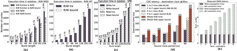
Figure 8 compares the maximum experimental delay measured for each component of the platform on serving a transaction (read and write) issued by with the upper bound proposed in Section 4 for different configurations. For these experiments, we set to issue 100’000 transactions, randomly selecting the burst length (). We monitor the service times, and then pick the longest ones.
Figure 8(a) reports the maximum service time of the main memory subsystem in case of a miss as a function of the burst length of the transaction under analysis, either when (i) only a refill is necessary and (ii) both refill and eviction are necessary, compared with the bounds proposed in Section 4.4. The measured service times are lower than the bounds. The pessimism is between 3% and 10.1% – the larger , the higher the pessimism. Higher pessimism on longer transactions is due to the internal splitting at the LLC. As from our analysis, the memory subsystem is not fully pipelined (). However, in practice, the control phase and the data phase of consecutive sub-transactions might be partially served in parallel by the LLC and the memory controller. This means that the longer the transaction, the higher the number of sub-transactions and their overlap, and the lower the service time when compared to our model. Thus, the pessimism increases. Figure 8(b) reports the measured results on the main memory subsystem but in case of a hit, compared with the bounds proposed in Section 4.2. As we consider an LLC hit, the access to the HyperRAM is not performed: this test analyzes the service time of the LLC. Our bounds always upper bound the maximum measured results. The trend here is reversed w.r.t. Figure 8(a) – as increases, the relative pessimism decreases from 7.7% down to 0.4%. In this case, the source of the pessimism comes only from the control time, which does not depend on , while there is no pessimism on the data time. Hence, this pessimism gets amortized as the burst length, and hence the overall service time, increases. We conduct the same experimental campaign also on the AXI SPM – the measured results, compared with the bounds proposed in Section 4.2, are reported in Figure 8(c). The trends are similar to the ones reported in Figure 8(b) for LLC hits – the pessimism of our analysis is limited to 1 and 2 clock cycles for reads and writes on the control time, respectively. As in the case of the LLC HITs, the upper bound on the control overhead gets amortized for longer transactions, and the pessimism reduces from 8.8% to 0.5%.
Figure 8(d) reports the maximum measured latency to cross an AXI CDC FIFO as a function of the manager clock period (the subordinate clock period is fixed to 30 ns), and compared with the bounds proposed in Section 4.1. The results are independent of the length of the transaction. To stimulate the highest variability, the phases of the clocks are randomly selected on a uniform distribution. The first bar reports the crossing delays from the manager side to the subordinate side, corresponding to the overall delays introduced on the AW, W, and AR AXI channels. The second bar reports the crossing delays from the subordinate side to the manager side, corresponding to the overall delays on the AXI R and B channels. The third bar shows the overall delay on a full transaction, corresponding to the sum of the two previously introduced contributions (see Section 4.1). The pessimism of our bounds is, at most, one clock cycle of the slowest clock between manager and subordinate.
Figure 8(e) reports the measured propagation delays introduced by the crossbar over an entire write and read transaction, compared with the bounds of Section 4.5, varying the number of controllers. As explained in Section 4.5, the propagation delay is the sum of the propagation latency without interference (eq. 14) and the additional contention latency (eq. 15), which depends on the number of controllers. Thanks to the simplicity of the arbitration operated by the crossbar (pure round-robin), our proposed bounds exactly match the measurements. We conducted the experimental campaign also on the IO subsystem. We measured the maximum service time and compared it with the upper bounds of Section 4.3, which we do not show for space reasons: such IP supports only single-word transactions. Our upper bounds exceed the maximum measured service time with pessimism of down to 2 clock cycles, with service times of 4 (write) and 5 (read) clock cycles.
6.1.2 Parallelism
To demonstrate our analysis on parallelism, we configured to issue unlimited outstanding transactions to the peripheral under test. In parallel, we monitor the maximum number of accepted outstanding transactions. We conducted tests on the analyzed peripherals and the crossbar. Our measurements match what is expected by our analysis, confirming that the maximum number of outstanding transactions is defined by the maximum parallelism accepted at the input stage of the peripherals and the crossbar.
6.2 System-level experiments
While the previous experiments focused on the evaluation at the IP-level, this set of experiments aims to evaluate the overall system-level bounds proposed in Section 5. We first validate our analysis in simulation, developing a System Verilog testbench with two configurable AXI synthetic (see Figure 1) and stimulating overload conditions highlighting worst-case scenarios. In the FPGA implementation, we leverage the traffic generated by the CVA6 core and the PULP cluster to validate our results.
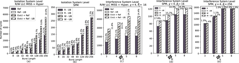
At first, we evaluate the results in isolation as a function of the burst length, leveraging the same strategy used for the previous experiments. Figures 9 (a) and (b) report the maximum measured system-level response times in isolation for completing a transaction issued by the generic controller and directed to (a) the main memory subsystem (case of cache miss, causing either refill or both refill and eviction) and (b) to the SPM memory, compared with the bounds proposed in Lemma 1. Again, the measured service times are smaller than the bounds in all of the tested scenarios. The measure and the trends reported in Figure 9(a) are aligned with the ones found at the IP level and reported in Figure 8(a). This is because the overhead introduced by the crossbar (in isolation) and the CDC FIFOs is negligible when compared to the service time of the memory subsystem. Figure 9(b) shows a trend aligned with the results at the IP-level reported in Figure 8(c) – the lower , the higher the pessimism. It is worth mentioning that the pessimism of the analysis at the system level is slightly higher w.r.t. the analysis proposed at the IP level. This is because the pessimism measured at the crossbar level (where we count the arbitration, not happening in this case) and at the CDC level is overall of 4 and 5 cycles for reads and writes and is added to 1 and 2 clock cycles at the IP level, respectively. This constant pessimism is amortized on longer transactions, down to 1.9%.
We now analyze the results under maximum interference. Figures 9 (c), (d), and (e) report the maximum measured system-level response times for completing a transaction issued by the generic controller and directed to (c) the main memory with an LLC miss considering , (d) the SPM memory, considering , and (e) the SPM memory, considering , and compare them with the upper bounds proposed in equation 20. For these tests, the execution of is interfered with by the controller – is fixed and equal to , while we vary the amount of outstanding transactions can issue ().
Figures 9 (c), (d), and (e) verify the results of Lemma 2 and 3: when (two bars on the right), the total service time is defined by the parallelism of the peripheral itself – as expected, after saturating the number of interfering transactions accepted by the peripheral, the measured results are the same regardless of the increase of . Differently, when , a reduced value of correspond to lower interference and response times. Figure 9(c) refers to the case of an LLC miss under interference when . The results confirm the safeness of our analysis, which correctly upper bounds the overall response times with a pessimism around , which is slightly higher than the pessimism of a transaction in isolation at the system level. As explained in the previous subsection, this is because when multiple transactions are enqueued, the memory subsystem is partially able to serve in parallel their data and control phases. However, our model only allows or , i.e., either the peripheral is fully pipelined or not pipelined at all. Since , the pessimism is slightly higher when more transactions are enqueued (and partially served in parallel) as equation 19 counts the service time of a transaction fully when . Varying of gives comparable results – we do not report such results for briefness and lack of space. We provide two charts for the SPM, in Figure 9(d) and Figure 9(e). The comparison of the two charts highlights how the length of the interfering transactions impacts the pessimism of the analysis, ranging between for to for . The trend here is aligned with the service time at the system level in isolation: the pessimism comes from the control times of SPM and propagation latency of the crossbar and the CDC, which are then amortized when the data time increases with .
7 Related Work
| Target | Analysis on | Pessimism | Technology | Open RTL | |
| Biondi et. al. [9] | ARM MPAM Protocol | Protocol specs (Model) | No HW | ✗ | ✗ |
| Hassan et. al. [6] | JEDEC DDR3 Protocol | Protocol specs (Model) | ✗ | ✗ | |
| BlueScale [10] | Hier. mem. IC | IC uArch (Black-box) | DMR | FPGA | ✗ |
| AXI-RT-IC [1] | AXI SoC IC | IC uArch (Black-box) | DMR | FPGA | ✗ |
| Restuccia et. al. [11] | AXI Hier. mem. IC | IC uArch (Black-box) | FPGA | ✗ | |
| Ditty [12] | Cache coher. mechanism | IP (Fine-grained RTL) | FPGA | ✓ | |
| This Work | SoC IC, peripherals & system-level | IP & System (Fine-grained RTL) | FPGA & ASIC | ✓ |
The majority of works on modeling and analysis leverage commercial off-the-shelf devices[35, 32] or predictable architectures modeled with a mix of cycle-accurate and behavioral simulators[36]. These works mainly focus on bounding the execution times for predefined specific software tasks rather than the individual transaction service times[35, 37, 36], limiting the generality of their approach. Furthermore, these works build the models from dynamic experiments rather than from static analysis, largely due to the dearth of detailed hardware specifications[33]. Our work breaks from this convention, presenting a holistic static model of the entire architecture rigorously validated through cycle-accurate simulation or FPGA emulation. Table I compares our approach with similar works advocating static modeling and analysis of protocols, interconnect, and shared memory resources to enhance the predictability of digital circuits. Biondi et al. [9] developed a model of the memory-access regulation mechanisms in the MPAM protocol by ARM and provided detailed instantiations of such mechanisms, which they then evaluated with IBM CPLEX, a decision optimization software for solving complex optimization models. While elegant, this approach is not validated on hardware and, therefore, is limited in terms of applicability and precision. A more practical and widely adopted approach is the one proposed by Hassan and Pellizzoni[6]. The authors develop a fine-grained model of the JEDEC DDR3 protocol, validated with Mcsim[8], which is a cycle-accurate C++ memory controller simulator. Unfortunately, not having access to the RTL prevents fine-grained modeling, analysis, and development and mandates over-provisioning, strongly impacting the overall pessimism of the system, which can be as high as 200%.
More recently, different researchers proposed models of hardware IPs that they could validate through cycle-accurate experiments [11, 1, 2]. In [11], Restuccia et al. focused on upper bounding the response times of AXI bus transactions on FPGA SoCs through the modeling and analysis of generic hierarchical interconnects arbitrating the accesses of multiple hardware accelerators towards a shared DDR memory. In this work, the interconnect under analysis is a proprietary Xilinx IP, which had to be treated as a black box. Also, due to the unavailability of the RTL code, the authors did not model the other IPs composing the target platform, limiting the precision of the proposed upper bounds, which achieve a pessimism between 50% and 90%. Jiang et al. modeled, analyzed, and developed AXI-IC[1] and Bluescale[10], two sophisticated interconnects providing predictability features and coming with a comprehensive model. However, the model and analysis proposed in AXI-IC[1], and Bluescale[10] are not as fine-grained as ours: the authors do not provide upper bounds of the access times but rather focus on the deadline miss ratio given a fixed workload for the different controllers in the system. Moreover, the authors do not provide the RTL of such solutions. In Ditty [12], researchers propose an open-source predictable directory-based cache coherence mechanism for multicore safety-critical systems that guarantees a worst-case latency (WCL) on data accesses with almost cycle-accurate precision. However, Ditty’s model only covers the coherency protocol latency and the core subsystem, overlooking system-level analysis and achieving very pessimistic boundaries. In this landscape, it emerges clearly that our work is the first one covering both modeling and analysis of the interconnects and the shared memory resources, with an in-depth analysis of silicon-proven open-source RTL IPs and achieving the lowest pessimism when compared to similar SoA works.
8 Conclusions
In conclusion, in this work, we showed (i) a novel fine-grained model for the typical resources composing modern heterogeneous low-power SoCs, (ii) a fine-grained analysis aligned with this model, and (iii) a full mathematical analysis to upper bound the response time of the interactions between controllers and shared peripherals, considering the maximum interference generated by the interfering controllers. Furthermore, our work is fully based on open-source IPs, allowing us to provide a worst-case analysis that is cycle-accurate, enabling direct verification of the analysis on the hardware.
After this thorough evaluation, we envision extending our results to more advanced Cheshire-based SoCs, with several hardware accelerators and a multi-core cache-coherent host. To hopefully stimulate novel research contributions, we open-source a guide to replicate the results shown in Section 6 at https://github.com/pulp-platform/soc_model_rt_analysis, comprehensive of the simulated environment and the software benchmarks to run on Carfield[38], a sophisticated Cheshire-based SoC targeting automotive applications.
References
- [1] Z. Jiang et al., “AXI-ICRT RT : Towards a Real-Time AXI-Interconnect for Highly Integrated SoCs,” IEEE Transactions on Computers, vol. 72, no. 3, pp. 786–799, 2022.
- [2] F. Restuccia et al., “AXI HyperConnect: A Predictable, Hypervisor-level Interconnect for Hardware Accelerators in FPGA SoC,” in 2020 57th ACM/IEEE Design Automation Conference (DAC), 2020.
- [3] A. Biondi et al., “SPHERE: A multi-SoC architecture for next-generation cyber-physical systems based on heterogeneous platforms,” IEEE Access, vol. 9, pp. 75 446–75 459, 2021.
- [4] L. Valente et al., “Shaheen: An Open, Secure, and Scalable RV64 SoC for Autonomous Nano-UAVs,” in 2023 IEEE Hot Chips 35 Symposium (HCS), 2023, pp. 1–12.
- [5] G. Fernandez et al., “Contention in multicore hardware shared resources: Understanding of the state of the art,” in Proceedings of the 14th International Workshop on Worst-Case Execution Time Analysis (WCET 2014), 2014, pp. 31–42.
- [6] M. Hassan and R. Pellizzoni, “Bounding DRAM Interference in COTS Heterogeneous MPSoCs for Mixed Criticality Systems,” IEEE Transactions on Computer-Aided Design of Integrated Circuits and Systems, vol. 37, no. 11, pp. 2323–2336, 2018.
- [7] M. Hassan, “On the Off-Chip Memory Latency of Real-Time Systems: Is DDR DRAM Really the Best Option?” in 2018 IEEE Real-Time Systems Symposium (RTSS), 2018, pp. 495–505.
- [8] R. Mirosanlou, D. Guo, M. Hassan, and R. Pellizzoni, “Mcsim: An extensible dram memory controller simulator,” IEEE Computer Architecture Letters, vol. 19, no. 2, pp. 105–109, 2020.
- [9] M. Zini, D. Casini, and A. Biondi, “Analyzing Arm’s MPAM From the Perspective of Time Predictability,” IEEE Transactions on Computers, vol. 72, no. 1, pp. 168–182, 2023.
- [10] Z. Jiang et al., “BlueScale: a scalable memory architecture for predictable real-time computing on highly integrated SoCs,” in Proceedings of the 59th ACM/IEEE Design Automation Conference, 2022, pp. 1261–1266.
- [11] F. Restuccia et al., “Bounding Memory Access Times in Multi-Accelerator Architectures on FPGA SoCs,” IEEE Transactions on Computers, vol. 72, no. 1, pp. 154–167, 2022.
- [12] Z. Wu, M. Bekmyrza, N. Kapre, and H. Patel, “Ditty: Directory-based Cache Coherence for Multicore Safety-critical Systems,” in 2023 Design, Automation & Test in Europe Conference & Exhibition (DATE). IEEE, 2023, pp. 1–6.
- [13] A. Herrera, “The Promises and Challenges of Open Source Hardware,” Computer, vol. 53, no. 10, pp. 101–104, 2020.
- [14] A. Ottaviano, T. Benz, P. Scheffler, and L. Benini, “Cheshire: A Lightweight, Linux-Capable RISC-V Host Platform for Domain-Specific Accelerator Plug-In,” IEEE Transactions on Circuits and Systems II: Express Briefs, pp. 1–1, 2023.
- [15] M. B. Taylor, “Your Agile Open Source HW Stinks (Because It Is Not a System),” in 2020 IEEE/ACM International Conference On Computer Aided Design (ICCAD), 2020, pp. 1–6.
- [16] PULP, “PULP Platform Github,” https://github.com/pulp-platform, 2022.
- [17] L. Valente et al., “HULK-V: a Heterogeneous Ultra-low-power Linux capable RISC-V SoC,” in 2023 Design, Automation & Test in Europe Conference & Exhibition (DATE), 2023, pp. 1–6.
- [18] OpenHW-Group, “CVA6,” https://github.com/openhwgroup/cva6, 2022.
- [19] M. Schneider et al., “Composite Enclaves: Towards Disaggregated Trusted Execution,” IACR Transactions on Cryptographic Hardware and Embedded Systems, vol. 2022, no. 1, p. 630–656, Nov. 2021.
- [20] P. Platform, “PULP cluster,” https://github.com/pulp-platform/pulp_cluster, 2022.
- [21] OpenHW-Group, “CV32E40P,” https://github.com/openhwgroup/cv32e40p, 2023.
- [22] A. Kurth et al., “An Open-Source Platform for High-Performance Non-Coherent On-Chip Communication,” IEEE Transactions on Computers, pp. 1–1, 2021.
- [23] B. John, “HyperRAM as a low pin-count expansion memory for embedded systems,” https://www.infineon.com/dgdl/Infineon-HyperRAM_as_a_low_pin-count_expansion_memory_for_embedded_systems-Whitepaper-v01_00-EN.pdf?fileId=8ac78c8c7d0d8da4017d0fb28970272c&da=t, 2020.
- [24] AMD, “Zynq-7000 - Technical Reference Manual, UG585,” https://docs.xilinx.com/r/en-US/ug585-zynq-7000-SoC-TRM.
- [25] AMD, “Zynq-UltraScale+ - Technical Reference Manual, UG1085,” https://docs.xilinx.com/r/en-US/ug1085-zynq-ultrascale-trm.
- [26] A. Noami, B. Pradeep Kumar, and P. Chandrasekhar, “High Performance AXI4 Interface Protocol for Multi-Core Memory Controller on SoC,” in Data Engineering and Communication Technology, K. A. Reddy, B. R. Devi, B. George, and K. S. Raju, Eds. Singapore: Springer Singapore, 2021, pp. 131–140.
- [27] ARM, “AMBA AXI Protocol Specification,” https://developer.arm.com/documentation/ihi0022/j/?lang=en, 2022.
- [28] Xilinx-AMD, “Dual Port SRAM specifications,” https://docs.xilinx.com/r/2022.1-English/ug1483-model-composer-sys-gen-user-guide/Dual-Port-RAM.
- [29] PULP, “HyperRAM Controller RTL,” https://github.com/pulp-platform/hyperbus, 2022.
- [30] Infineon, “HyperRAM RTL,” https://www.infineon.com/dgdl/Infineon-S27KL0641_S27KS0641_VERILOG-SimulationModels-v05_00-EN.zip?fileId=8ac78c8c7d0d8da4017d0f6349a14f68, 2022.
- [31] Infineon, “HyperBUS specifications,” https://www.infineon.com/dgdl/Infineon-HYPERBUS_SPECIFICATION_LOW_SIGNAL_COUNT_HIGH_PERFORMANCE_DDR_BUS-AdditionalTechnicalInformation-v09_00-EN.pdf?fileId=8ac78c8c7d0d8da4017d0ed619b05663, 2022.
- [32] R. Wilhelm et al., “The worst-case execution-time problem—overview of methods and survey of tools,” ACM Trans. Embed. Comput. Syst., vol. 7, no. 3, may 2008. [Online]. Available: https://doi.org/10.1145/1347375.1347389
- [33] T. Mitra, J. Teich, and L. Thiele, “Time-critical systems design: A survey,” IEEE Design & Test, vol. 35, no. 2, pp. 8–26, 2018.
- [34] F. Restuccia et al., “Modeling and analysis of bus contention for hardware accelerators in FPGA SoCs,” in 32nd Euromicro Conference on Real-Time Systems (ECRTS 2020). Schloss Dagstuhl-Leibniz-Zentrum für Informatik, 2020.
- [35] J. P. Cerrolaza et al., “Multi-Core Devices for Safety-Critical Systems: A Survey,” ACM Comput. Surv., vol. 53, no. 4, aug 2020. [Online]. Available: https://doi.org/10.1145/3398665
- [36] M. Schoeberl et al., “T-CREST: Time-predictable multi-core architecture for embedded systems,” Journal of Systems Architecture, vol. 61, no. 9, pp. 449–471, 2015.
- [37] G. Fernandez et al., “Increasing confidence on measurement-based contention bounds for real-time round-robin buses,” in Proceedings of the 52nd Annual Design Automation Conference, ser. DAC ’15. New York, NY, USA: Association for Computing Machinery, 2015.
- [38] PULP, “Carfield,” https://github.com/pulp-platform/carfield.
| Luca Valente received the MSc degree in electronic engineering from the Politecnico of Turin in 2020. He is currently a PhD student at the University of Bologna in the Department of Electrical, Electronic, and Information Technologies Engineering (DEI). His main research interests are hardware-software co-design of heterogeneous SoCs. |
| Francesco Restuccia received a PhD degree in computer engineering (cum laude) from Scuola Superiore Sant’Anna Pisa, in 2021. He is a postdoctoral researcher at the University of California, San Diego. His main research interests include hardware security, on-chip communications, timing analysis for heterogeneous platforms, cyber-physical systems, and time-predictable hardware acceleration of deep neural networks on commercial FPGA SoC platforms. |
| Davide Rossi received the Ph.D. degree from the University of Bologna, Bologna, Italy, in 2012. He has been a Post-Doctoral Researcher with the Department of Electrical, Electronic and Information Engineering “Guglielmo Marconi,” University of Bologna, since 2015, where he is currently an Associate Professor position. His research interests focus on energy-efficient digital architectures. In this field, he has published more than 100 papers in international peer-reviewed conferences and journals. |
| Ryan Kastner is a professor in the Department of Computer Science and Engineering at UC San Diego. He received a PhD in Computer Science at UCLA, a masters degree in engineering and bachelor degrees in Electrical Engineering and Computer Engineering from Northwestern University. His current research interests fall into three areas: hardware acceleration, hardware security, and remote sensing. |
| Luca Benini holds the chair of digital Circuits and systems at ETHZ and is Full Professor at the Università di Bologna. He received a PhD from Stanford University. Dr. Benini’s research interests are in energy-efficient parallel computing systems, smart sensing micro-systems and machine learning hardware. He has published more than 1000 peer-reviewed papers and five books. He is a Fellow of the ACM and a member of the Academia Europaea. |