SiPM understanding using simple Geiger-breakdown simulations
Abstract
The results of a 1-D Monte-Carlo program, which simulates the avalanche multiplication in diodes with depths of the order of 1 m based on the method proposed in Ref. [1], are presented. The aim of the study is to achieve a deeper understanding of silicon photo-multipliers. It is found that for a given over-voltage, , the maximum of the discharge current is reached at the breakdown voltage, , and that the avalanche stops when the voltage drops to . This is completely different to the generally accepted understanding of SiPMs, which has already been noted in Ref. [1]. Simulated characteristics of the avalanche breakdown, like the time dependence of the avalanche current, over-voltage dependence of the Geiger-breakdown probability and the gain for photons and dark counts, are presented and compared to the expectations from silicon photo-multipliers.
keywords:
Silicon photomultipliers , Geiger breakdown , simulations.1 Introduction
SiPMs (Silicon Photo-Multipliers), matrices of avalanche photo-diodes, called pixels in this paper, operated above the breakdown voltage, are the photo-detectors of choice for many applications. They are robust, have single photon resolution, high photon-detection efficiency, operate at voltages below 100 V and are not affected by magnetic fields. In this paper an attempt is made to explain several of the experimentally observed properties of SiPMs with the help of a Monte Carlo simulation of the time dependence of the avalanche of a single pixel.
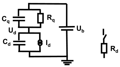
Fig. 1 shows an electrical diagram of a single pixel biased to the voltage . The avalanche region has the capacitance and the current source generates the avalanche current, . The avalanche region is coupled to the power supply via the quenching resistor, , which quenches the avalanche. During the avalanche, the voltage over the avalanche region, , decreases until the avalanche stops and there are no free charge carriers left in the avalanche region. Then, recovers to with the time constant . The recharging of represents the main pulse of the SiPM. Parallel to there can be a quenching capacitance, , which produces a fast pulse component.
There is general agreement that this electrical scheme can be used to describe SiPMs. However, there are significantly different assumptions for both the time dependence of the discharge current, , as well as also for , the breakdown voltage above which avalanche breakdown occurs. In principle can be calculated using the ionization integral as discussed in section 2.1. However, neither the electric field distribution nor the ionization rates are sufficiently well known to yield reliable results. Therefore, is determined from current-voltage, gain-voltage or pde-voltage (photon detection efficiency) measurements using phenomenological parameterizations. Although the results for are typically consistent within 0.1 V, there are also difference of up to 1 V. Several authors ascribe these differences to a difference between the voltage at which Geiger discharges are possible, and the voltage at which the Geiger discharges stop (Ref. [2]). However, there is no consensus.
For the discharge current different ad hoc parameterizations can be found in the literature: One example is shown on the right side of Fig. 1: A switch which is open in the quiescent state, closes when the Geiger discharge starts, and opens again at the end of the Geiger discharge. The switch is connected to a discharge resistor, , followed by a voltage source , all in parallel to the capacitance . Typically, is equal to obtained as discussed above. Another approach is to remove the voltage source, close the switch at the start of the Geiger discharge, and open it again when is reached. In both cases, the values of the components have to be chosen so that the duration of the discharge is less than 1 ns. In this paper the time-dependent discharge current, , is simulated following the method of Ref. [1].
Next, the calculation of the breakdown voltage is discussed, followed by a presentation of the model used for the simulation of avalanches. Using the simulation, the time dependence of the discharge current and of the over-voltage dependence of the discharge current, of the Geiger-discharge probability and of the gain for photons and for dark counts, are evaluated. This is followed by the simulation of more than one discharge channel. Finally, the main results are summarized and further tests of the used model of avalanche simulation suggested.
2 Simulation method and results
In this section the simulation of the avalanche multiplication and Geiger breakdown is described, which follows the approach of Ref. [1].
Simulated is a single square pixel of depth and area , biased to the voltage and connected to the power supply by a quenching resistor . The value of is sufficiently large, so that current following through during the avalanche built-up, which takes less than 1 ns, can be ignored. The coordinate normal to the pixel surface is called . The 1D electric field, , points in the direction, with the voltages and . For the pixel capacitance is assumed, and couplings to neighbouring pixels are ignored.
2.1 Breakdown voltage
First, the breakdown voltage, , as a function of and of the absolute temperature, , is estimated by setting the Ionization Integral
| (1) |
equal to 1 [3]. The hole- and electron-ionization coefficients, and , which parameterize the mean number of electron-hole pairs generated for a 1 cm path, are functions of the electric field, , and of . The right-hand side of Eq. 1 gives the results for a constant field. The hole and electron ionization coefficients in silicon are only poorly known [4]. In addition, they do not take into account the "history" of the charge carriers responsible for the ionization, e.g. their momenta after the preceding interaction with the silicon lattice. This approach is a significant over-simplification, in particular for narrow amplification regions, as discussed in Ref. [5]. In this paper the van Overstraeten–de Man parametrization [6] is used, but it has been checked that other parameterizations give at least qualitatively similar results.
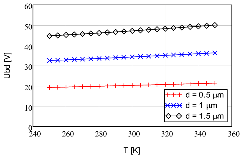
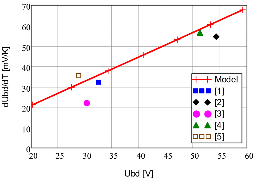
Fig.2 shows some results of the calculated and dependence of . As also observed experimentally, increases with and , and if is known the depth of the multiplication layer can be estimated. The calculations also confirm the observation that SiPMs with a higher have a higher . In Fig. 2(b) the result of the model calculation is compared to experimental data. Although there is a significant spread of the experimental values at a given , the overall dependence of is reproduced.
2.2 Simulation of the avalanche multiplication
In the most simple simulation, which is described next, a uniform electric field is assumed, with the time dependent voltage drop over the avalanche region. Initially , the bias voltage. The depth is divided into intervals of size . Given the high electric field, for both holes and electrons the saturation velocity cm/s ([3]) is assumed, which results in time steps for charge carriers to drift from one grid point to its neighbour. This assumption results in a significant simplification of the simulation. As both the impact ionisation and the induced charge can be considered as geometrical effects, which can be seen that the units of the ionisation coefficients and of the weighting field are 1/cm, the integral of the current is not affected by this assumption. Only the time dependence of the induced current is affected, which is found to be inversely proportional to . Typical values used in the simulation for m at V are: V/cm, , nm and ps.
Next, the simulation of a single avalanche is discussed. Initially an electron-hole pair is generated at one -grid point. Then the avalanche is iteratively calculated until there is less than one charge carrier in the multiplication region, when the simulation for this avalanche is stopped. The number of holes at position at the time step , , and the corresponding number of electrons, , are obtained from the number of holes and electrons at the positions at the time step it
| (2) |
| (3) |
where rpois() is a Poisson-distributed random number with the mean .
Eq. 2 can be understood in the following way: The first term describes the number of holes which drift by during the time , the second term the number of holes generated by the drifting holes, which also drift in the direction, and the third term the number of holes which are generated by the electrons which drift in the direction. This term assumes that the ionization by electrons takes place half way between the grid points. Similar arguments allow deriving Eq. 3 for electrons. To account for the charges flowing into the electrodes, and are set to zero after every iteration.
The avalanche current is obtained by the product of the total number of charge carriers, the elementary charge, , the drift velocity, , and the weighting field, :
| (4) |
Using the model shown in Fig. 1, the derivative, , is obtained from current conservation: The current in the quenching section has to be equal to the current in the avalanche section , which gives
| (5) |
where the right most expression is the limit for and , which is actually used in the simulations. It has been checked that this approximation is justified for realistic parameter values. Inserting Eq. 4 into the right-hand side of Eq. 5, and using for the time step of one iteration gives
| (6) |
where is the charge induced in iteration it and the voltage over the avalanche region at step . It is noted that time does not enter in this relation, which means that the method is insensitive to the assumption on the drift velocities.
2.3 Time structure of avalanche development
In this section the time dependence of the number of charge carriers in the amplification region, which is proportional to the current, and of the voltage are discussed. For the simulation an amplification region m and a constant electric field of strength pointing in the direction are assumed. At time an electron-hole pair is generated at m. The drift velocity of both electrons and holes is set to cm/s which results in a transit time of 10 ps. The calculated value of the breakdown voltage is 34.36 V for the assumed temperature of 300 K.
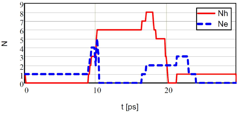
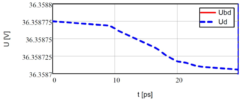
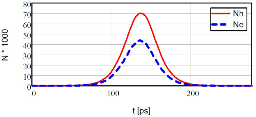
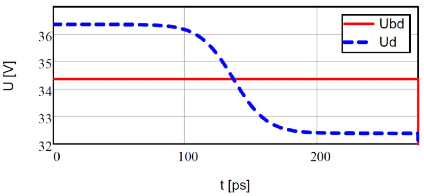
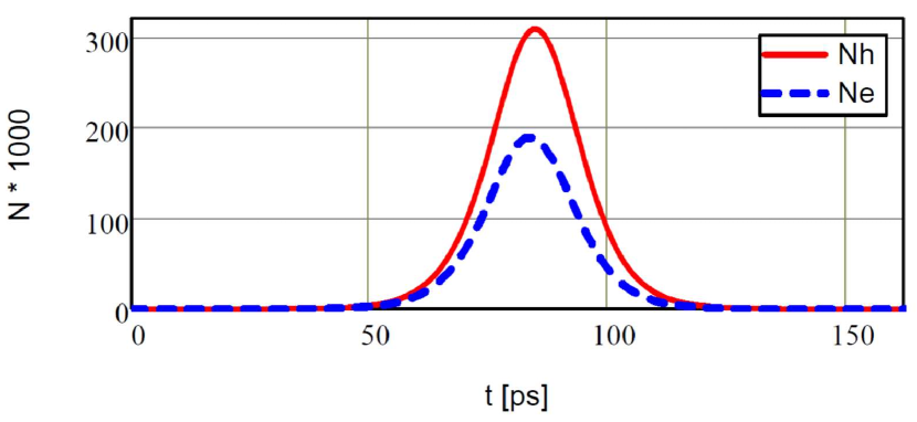
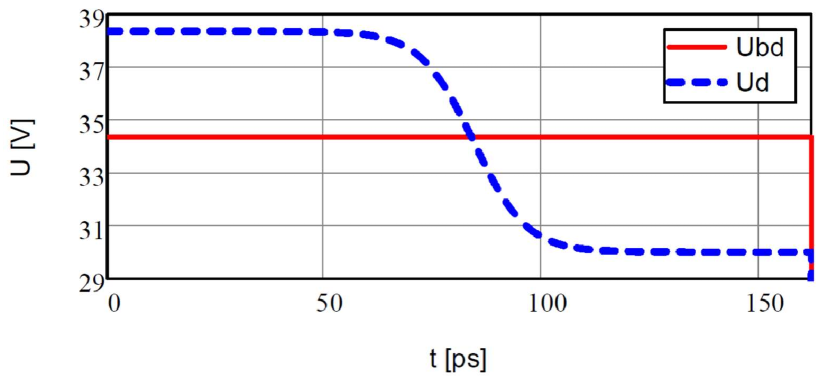
Fig. 3 shows for three simulated events the time dependence of the number of holes and electrons in the amplification region and the voltage over the amplification region. For the event on top, the over-voltage and no Geiger breakdown occurs. In Fig. 3(a) one can see the occurrences of the ionizations and of the arrival of the charge carriers at the electrodes. At the initial electron-hole pair is generated at m. The hole reaches the electrode after one time step of 0.1 ps (solid line) and there are no holes and only a single electron (dashed line) drifts in the amplification region until the ionization at ps. The ionization at 9 ps is followed by two close-by ionizations, so that shortly before the transit time of 10 ps there are three holes and four electrons, all close to in the amplification region. The drop of the number of electrons from four to two is caused by two electrons reaching the electrode at . Close to ps there are three more ionizations and the number of holes increases from three to six. As these ionizations occur close to the electrons reach the electrode within about 1 ps, and, until the ionization at 16 ps, six holes and zero electrons drift in the amplification region. The further development of the number of charge carriers can be easily followed, until at ps no more charge carriers are left. Including the primary ionization there are 10 ionizations. Thus the gain for this event is ten, and the expected voltage drop over the pixel, using the relation , is V, where pF is the capacitance of a m m pixel with a depth of m has been used. This overall voltage drop is confirmed by the time dependence of which is shown in Fig. 3(b).
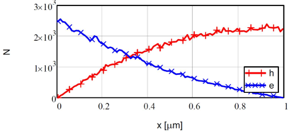
Fig. 3(c) shows the time dependence of the number of charge carriers, , for an event with the same initial conditions as in the figure above. However, in this event a Geiger discharge has occurred. As discussed in detail in Ref. [1], after an initial time interval with large fluctuations there is an exponential increase of until , followed by an exponential decrease until is reached (see Fig. 3(d)). The gain for this event is , the maximum of occurs at ps and the full width at half maximum is 35 ps. The value of reached at the end of the Geiger discharge is 32.25 V, which is 2.11 V below V. As already discussed in Ref. [1], the result of the simulation, that the Geiger discharge stops at and that the gain is which is completely different from the generally accepted understanding that the Geiger discharge stops at and that the gain is , as discussed for example in Ref. [10]. So far this issue has not been resolved. It is also noted that holes have a bigger contribution to the signal than electrons. The reason is that during the discharge the number of electrons increases towards and therefore the mean path of the holes from ionization, which drift to , is larger than for electrons. This is demonstrated in Fig. 4 which shows the dependence of holes and electrons at the maximal current of the Geiger discharge.
On the bottom of Fig. 3 the results for a Geiger breakdown at V are shown. Qualitatively, the time dependencies is similar to the breakdown at V. However, the maximum of is at ps and the full width at half maximum is 23 ps. The gain is , which is again , and the value of reached at the end of the Geiger discharge is 30.02 V.
Simulations for different values of the depth of the depletion layer show that with increasing the gain decreases, because of the reduced pixel capacitance, and that both the time of the maximum of and the full width at half maximum of increase.
One prediction of the simulation is that after a Geiger discharge for times where is the time constant of the recharging of the pixel. is the resistance of the quenching resistor and the capacitance of the avalanche region. Typical values for are in the range of 10 ns to 100 ns. As a consequence, after-pulses should appear only for . Inspection of Refs [11, 7, 12] shows that so far after-pulses have only been measured for values greater than several tens of nanoseconds, and therefore this prediction of the simulation has not been tested so far.
2.4 Over-voltage dependence of the SiPM current, the breakdown probability and the gain
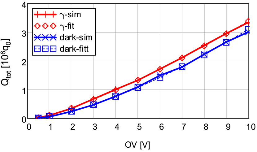
In this section the results of the simulations for photons and dark counts and avalanche regions of mm area with depths of 0.5, 1.0 and 1.5 m as a function of the over-voltage are presented. Photons with a wavelength of 350 nm, which have an attenuation length of about 10 nm in silicon, are simulated by generating the primary electron-hole pairs at m, and dark counts by generating the primary electron-hole pairs uniformly over all values. For every over-voltage 1000 events are simulated. Fig. 5(a) shows to total SiPM charge, . The simulations include events without and with Geiger discharges. The voltage dependencies can be fitted by the function
| (7) |
where is the over-voltage of the intercept of the fitted curve with the abscissa, is the mean charge for , and characterizes the increase of with . The values of the fitted parameters for the simulations with , 1 and 1.5 m are shown in Table 1. In all cases the fits describe the data within their statistical uncertainties.
| m] | [V] | [mV] | [V] | [mV] | ||
|---|---|---|---|---|---|---|
| 0.5 | ||||||
| 1.0 | ||||||
| 1.5 | ||||||
| 0.5 | ||||||
| 1.0 | ||||||
| 1.5 |
It is noted that is closely related to the voltage dependence of the SiPM current: If the rate of photons, , and the contribution from cross-talk and after-pulses, XT(OV), are known, the photo-current can be calculated by multiplying simulated for photons with ; if has been measured, XT(OV) can be estimated. Similar relations hold for the dark-current, .
Fig. 5(a) shows that , i.e. the integral of the current per initial electron-hole pair, is larger for photons than for dark counts. The reason is that the Geiger-breakdown probability decreases with distance from the position at which the photons enter. Whereas 350 nm photons convert within about 10 nm, the dark counts are approximately uniformly distributed in the amplification region. The values for , given in Table 1, show that voltage dependence of is steeper than for , which is also observed experimentally. The simulated values have no significant dependence on the breakdown voltage. For a value of mV is found, which is about three standard deviations larger than zero for all simulations. It is noted that the value of obtained from the ionization integral may be different from the values in the literature, which are experimentally determined using different prescriptions, as discussed e.g. in Refs. [2, 10].
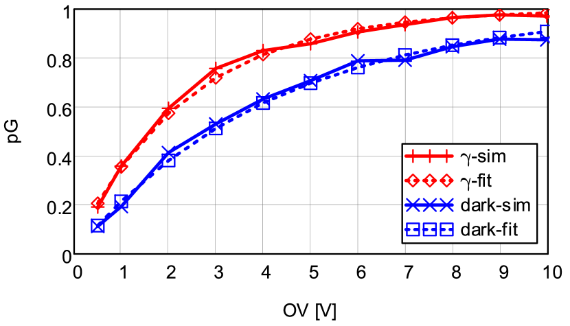
Events without and with Geiger discharges are well separated both in charge and in the time of the maximum of the discharge current. From the ratio of the number of events with a Geiger discharge to the total number of simulated event, the Geiger-discharge probability, pG(OV), is determined. Fig. 5(b) shows the results for m for photon- and dark-count-induced events together with fits by
| (8) |
where is the over-voltage of the intercept of the fitted curve with the abscissa, and the characteristic voltage of pG(OV). The values of the fitted parameters for the simulations with , 1 and 1.5 m are shown in Table 1. In all cases the fits describe the data within their statistical uncertainties.
As expected, the Geiger-breakdown probability, , shown in Fig. 5(b) for m, is significantly larger for photons than for dark-counts: At V it is by a factor 2 bigger, and at V the values are 98.5 % and 87.5 %, respectively. The values of reported in Table 1, which describe the increase of pG with OV, increase with and are significantly larger for dark-counts than for photons. Similar values and a similar increase have been reported by several authors, e.g. in Refs. [7, 13]. The values of are small and within their fairly large statistical uncertainties compatible with zero. It can be concluded, that the breakdown voltage can be determined from a fit to pG(OV).
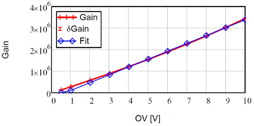
The simulated over-voltage dependence of the gain for photons, which is the mean charge in units of elementary charges for the events with Geiger discharges, is shown in Fig. 6 for an amplification region of m. The crosses are the simulations and the diamonds the results of a straight-line fit for V. The values simulated for photons and for dark counts are statistically compatible, and only the results for photons are shown.
Different to the results from measurements, significant deviations from linearity are observed at low over-voltages and the intercept with the abscissa is at V, which casts doubts on the validity of the simulation. The simulations for m and for m show a similar non-linearity. In order to check if, ignoring the currents flowing through and (see Fig. 1) are responsible for the non-linearity, Eq. 5 with k and fC has been used for the simulation. However, the non-linearity remains. Also changing the step, , from 10 nm to 5 nm and 20 nm, the saturation velocity, , from cm/s to cm/s and cm/s, and multiplying the ionization coefficients, and , by 0.75 and by 1.5 separately and combined, do not change the Gain–OV dependence.
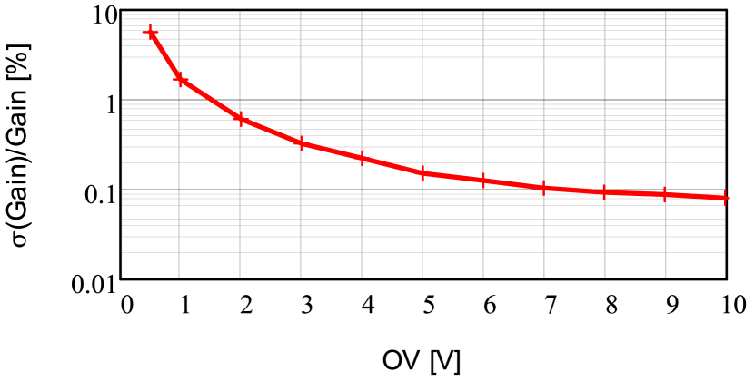
The careful inspection of Fig. 5b of Ref. [1], which shows for and 3 V and m the time dependence of the voltage over the avalanche region during the Geiger discharge, shows a similar effect: Whereas for V the voltage swing is compatible with , the voltage swing for V is larger than . This is in complete agreement with the simulations of this paper. It is thus concluded that with respect to the linearity of the mean gain as a function of over-voltage, the simulation fails to describe the experimental data. In Fig. 6(b) the over-voltage dependence of the relative rms width of the gain-distribution is shown. For V it exceeds 5 %, but decreases rapidly and attains values below 0.1 % above V. The results of the simulations with m and m are similar.
2.5 Simulation with more than one discharge in a pixel for photons
In this section two separate avalanches generated by two ionizations, separated in time by , are simulated. The question addressed is: Does the Geiger-discharge probability and the gain depend on ? Such a dependence could explain the observation reported e.g. in Ref. [14] that for sub-nanosecond light pulses the response of SiPMs does not saturate at the value: Number of pixels times the response of a single Geiger discharge.
The simulation proceeds as discussed in section 2.2. The electron-hole pairs are generated at m, the first at and the second at . The two avalanches are simulated separately but, for calculating , the number of holes and electrons from both avalanches are added.
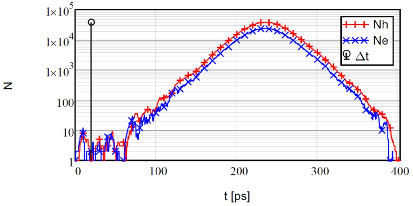
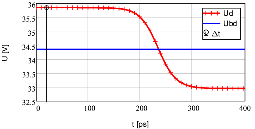
Fig. 7 shows in logarithmic scale the time dependence (a) of the number of holes and electrons, and (b) of for m and V for two ionizations at m, the first at and the second at ps. The distributions are similar to the ones of avalanches induced by a single ionization shown in Fig. 3.
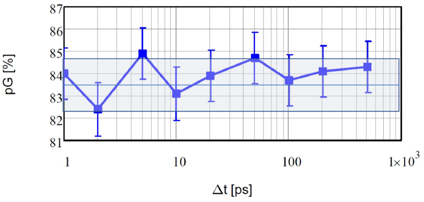
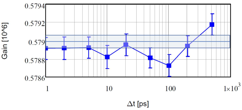
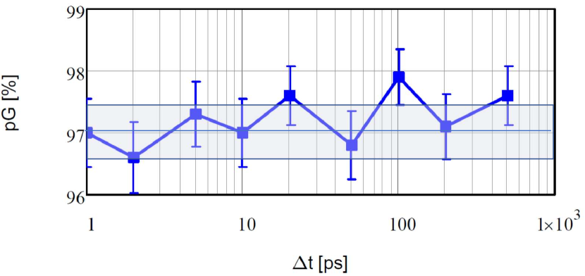
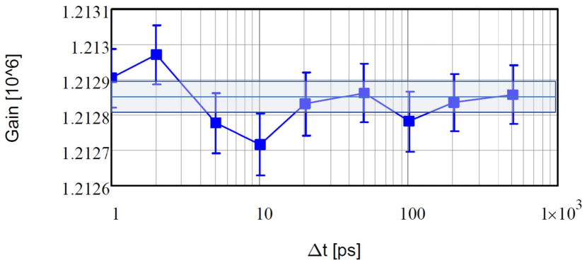
Figs 8 and 9 show as a function of the Geiger-discharge probability and the gain for over-voltages of 2 V and 4 V, respectively. Neither Geiger-discharge probability nor gain depend on , and thus do not provide an explanation for the observed saturation behaviour of SiPMs exposed to sub-nanosecond light pulses. As shown by the shaded bands, the gain for one and for two ionizations by photons is the same. The Geiger-discharge probability for photons, can be estimated from the Geiger-discharge probability for 1 photon, ,
| (9) |
where is the probability that none of the photons resulted in a Geiger discharge. As shown by the shaded bands in Figs 8(a) and 9(a), the simulations agree with this relation.
3 Summary and conclusions
The time development of avalanches in narrow (order m) multiplication regions biased above the breakdown voltage has been simulated with the aim to better understand the functioning of SiPMs.
The method of Ref. [1] has been used.
It is found that the results differ significantly from the generally accepted understanding of SiPMs:
The avalanche does not stop when the voltage over the amplification region is close to the breakdown voltage, , but when it is , where the over-voltage, , is the difference between the bias voltage minus .
As a result the predicted gain is instead of (elementary charge ), and no after-pulses are predicted for times , when the voltage over the amplification region after a discharge at starts to exceed ; is the capacitance of the multiplication region and the recharging time constant.
So far it has not been studied which prediction agrees with experimental data.
The simulations explain a number of experimental findings:
-
1.
The avalanche breakdown happens within less than 1 ns.
-
2.
Both dark- and photo-current are proportional to , where has only a weak dependence and is larger for the dark- than for the photo-current.
-
3.
The OV dependence of the Geiger-breakdown probability can be described by , where increases with ; is smaller for photons which generate electron-hole pairs close to the surface, than for dark counts with an approximately uniform distribution over the avalanche region.
However, there is a major disagreement with experimental results: The dependence of the gain on OV is non-linear at small over-voltages, and the extrapolation from the linear region ( V) reaches gain = 1 at V. This casts doubts on the validity of the simulation.
As the model differs drastically from the generally accepted understanding of Geiger breakdown in SiPMs, more predictions should be compared to experimental data. In particular the question if the gain is or twice this value, and if after-pulses appear shortly after the Geiger breakdown or not, should be settled by experiments. It is also noted that the SiPM response and its simulation, in particular in the non-linear regime, differs for the two models: For the generally accepted model the time delay between Geiger discharges in the same pixel for high photon intensities and/or high dark-count rates starts essentially at zero, whereas for the model discussed in this paper, it only starts once the voltage over the avalanche region exceeds the breakdown voltage.
References
- [1] P. Windischhofer and W. Riegler, Passive quenching, signal shapes and space charge effects in SPADs and SiPMs, Nucl. Instr. and Meth. A 1045 (2023) 167627.
- [2] V. Chmill et al., Study of the breakdown voltage of SiPMs, Nucl. Instr. and Meth. A 845 (2016) 56 –59.
- [3] S.M. Sze, Physics of Semiconductor Devices, John Wiley & Sons.
- [4] E.C. Rivera and M. Moll, Study of Imapct Ionization Coefficients in Silicon with Low Gain Avalanche Diodes, IEEE Transactions on Electron Devices, Vol. 70, No. 6, June 2023, pp. 2919–2926.
- [5] R.J. McIntyre, A New Look at Impact Ionization – Part I: A Theory of Gain, Noise, Breakdown Probability, and Frequency Responnse, IEEE Transactions on Electron Devices, Vol. 46, No. 8, August 1999, pp. 1623–1631.
- [6] R. van Overstraeten and H. de Man, Measurement of the ionization rates in diffuse silicon p-n junctions, Solid-State Electronics 13 (1975) 583 –608.
- [7] A.N. Otte, D. Garcia, T. Ngyen, D. Purushotham, Characterisation of three High-Efficiency and blue sensitive Silicon Photomultipliers, Nucl. Instr. and Meth. A 846 (2017) 106 –1255.
- [8] R. Parsiani et al., Characterisation of Hamamatsu S13161-3050AE-08 SiPM () array at different temperatures with CAEN DT5202, Nucl. Instr. and Meth. A 1057 (2023) 167632.
- [9] M. Mazillo et al., Silicon Photomultipliers for nuclear medical imaging appliccations, Proc. of SPIE Vol. 7003 (2008) 70030I 1–11.
- [10] R. Klanner, Characterisation of SiPMs, Nucl. Instr. and Meth. A 926 (2019) 36 –56.
- [11] P. Eckert et al., Characterisation Studies of Silicon Photomultipliers, Nucl. Instr. and Meth. A 620 (2010) 217–226.
- [12] C. Piemonte and A. Gola, Overview on the main parameters and technology of modern Silicon Photomultipliers, Nucl. Instr. and Meth. A 926 (2019) 2 –15.
- [13] J. Rolph et al., A Python module for fitting charge spectra of Silicon Photomultipliers, Nucl. Instr. and Meth. A 1056 (2023) 168544.
- [14] Q. Weitzel et al., Measurement of the Response of Silicon Photomultipliers from single photon detection to saturation, Nucl. Instr. and Meth. A 936 (2019) 558 –560.