Wavelength dependence of nitrogen-vacancy center charge cycling
Abstract
Optically-active spin qubits in wide-bandgap semiconductors exist in several charge states, though typically only specific charge states exhibit desirable spin or photonic properties. An understanding of how interconversion between different charge states occurs is important for most applications seeking to employ such defects in quantum sensing and information processing, and additionally serves as a means of testing and verifying models of the defect electronic structure. Here, we use charge-sensitive confocal imaging to study the wavelength dependence of optical carrier generation in diamonds hosting nitrogen-vacancy (NV) centers, silicon vacancy (SiV) centers and substitutional nitrogen (N). We study the generation of distinctive charge-capture patterns formed when photogenerated charge carriers are captured by photoluminescent defects, using light spanning 405-633 nm (1.96-3.06 eV). We observe distinct regimes where one- or two-photon ionization or recombination processes dominate, and a third regime where anti-Stokes mediated recombination drives weak NV charge cycling with red light. We then compare red-induced charge cycling to fast charge carrier transport between isolated single NV centers driven with green and blue light. This work reports new optically-mediated charge cycling processes of the NV centers, and has consequences for schemes using charge transfer to identify non-luminescent defects and photoelectric detection, where ambiguity exists as to the source of photocurrent.
I Introduction
While many optically-active and spin-addressable defects exist in materials such as diamond [1, 2], silicon carbide [3] and hexagonal boron nitride [4, 5], the spin and photonic properties that are sought are often only associated with a particular charge state of the defect, which may in turn exhibit instability under optical addressing [6]. For instance, the neutral charge state of the nitrogen-vacancy (NV) center in diamond (NV0) with a zero-phonon line (ZPL) at 575 nm exhibits neither the spin-dependent fluorescence or long ground-state coherence times of the negatively-charged NV- (ZPL at 637 nm) that features prominently as a platform for quantum sensing and information processing [7]. Besides the NV center, many other defects exist with various charge states that exhibit photochromism, like the silicon-vacancy SiV-, SiV0 and SiV2- charge states [8, 9, 10]. On the other hand, other defects that are optically inactive, such as substitutional nitrogen which exists in N0, N+ and N- states [11] have important consequences for the charge stability and spin coherence of nearby color centers [12, 13, 14] due to their abundance.
Charge state measurement and control represents a powerful tool to augment and improve existing quantum measurement techniques [15] as well as facilitating new applications [16, 17, 18, 19, 20, 21, 22, 23], in particular, photoelectric detection of NV magnetic resonance [24, 25, 26]. It is in photoelectric detection that knowledge of the charge interconversion processes are most important, such as the role of other defects that contribute to the photocurrent [27, 28], particularly under varied excitation wavelengths [29]. Similarly, the role of freely diffusing charges generated by optical excitation has been examined in observation and control of the space-charge potentials accompanying the generation and diffusion of free carriers [30], identification of charge carriers from optical illumination of different defect species [31, 32], transport of charge carriers between single NV defects [33, 32, 34] and control over the charge environment-limited spin coherence of NV centers [13, 35, 14]
In this work, we investigate the photogeneration and capture of charge carriers in three diamond samples containing varying densities of nitrogen, NV centers, and SiV centers as a function of excitation wavelength. We study the formation of characteristic ‘halo’ patterns of carriers diffusing into charge environments tailored to specific defect concentrations via multi-wavelength scanning confocal microscopy. The range of excitation wavelengths we use span 405-633 nm, sufficient to observe single-photon mediated photoionization and recombination of NV centers in the blue (405-480 nm), two-photon charge cycling of the NV charge state (515-594 nm), and weak two-photon recombination of NV0 and near-resonant ionization of NV- (594, 633 nm), which we ascribe to phonon-assisted anti-Stokes excitation of the NV0 zero-phonon line (ZPL) transition. We do not find any evidence that SiV defects alone undergo charge cycling under optical illumination, even under red excitation, with silicon-free diamonds exhibiting essentially the same charge carrier generation as SiV-rich samples. We then show that red excitation of a single NV center mediates hole generation and capture by a second nearby single NV center, and compare this with carrier generation under blue and green light, observing carrier generation and transport rates an order of magnitude faster than previously reported [33]. Our work has important consequences for the study of charge carrier generation and capture in diamond, which spans photoelectric detection [26, 28], stabilization of defect charge states [36, 37] and the identification of photoactive and inactive defects [31, 32].
II Experiment
A simplified schematic of our experiment is depicted in Fig 1(a). We use a home-built scanning confocal microscope that features optical paths for excitation wavelengths ranging from 405 nm to 633 nm, which are directed into the back aperture of a 0.7 NA microscope objective mounted on a three-axis scanning piezoelectric stage. The different colors of light are sourced from a variety of fixed-wavelength diode or diode-pumped solid state lasers that are intensity controlled by either acousto-optic modulators (AOMs: 480 nm, 532 nm, 561 nm and 594 nm) or by directly varying the diode drive current (405 nm, 450 nm, 515 nm and 633 nm). Fluorescence from the diamond is collected by the same objective lens, directed through bandpass filters to isolate NV- emission (691-730 nm) and then focused by a 150 mm-focal-length achromatic lens into a m-core-diameter multimode fiber, where it is directed into a single-photon counting module.
The diamond samples we investigated were obtained from commercial suppliers, grown via chemical vapor deposition (CVD), and contain a natural abundance of 13C. Sample A is a [100]-cut electronic-grade commercial diamond from Element6 with [N] = ppm, [NV] = 10 ppb and no detectable SiV fluorescence. Sample B is a [111]-cut standard-grade sample from Delaware Diamond Knives with [N] = 1 ppm, [NV] = 10 ppb and [SiV] = 1 ppm (estimated). Aside from crystallographic orientation and SiV concentrations, the samples feature similar fluorescence levels under green illumination and similar spin coherence properties s, s), and feature nitrogen as the dominant impurity [38].
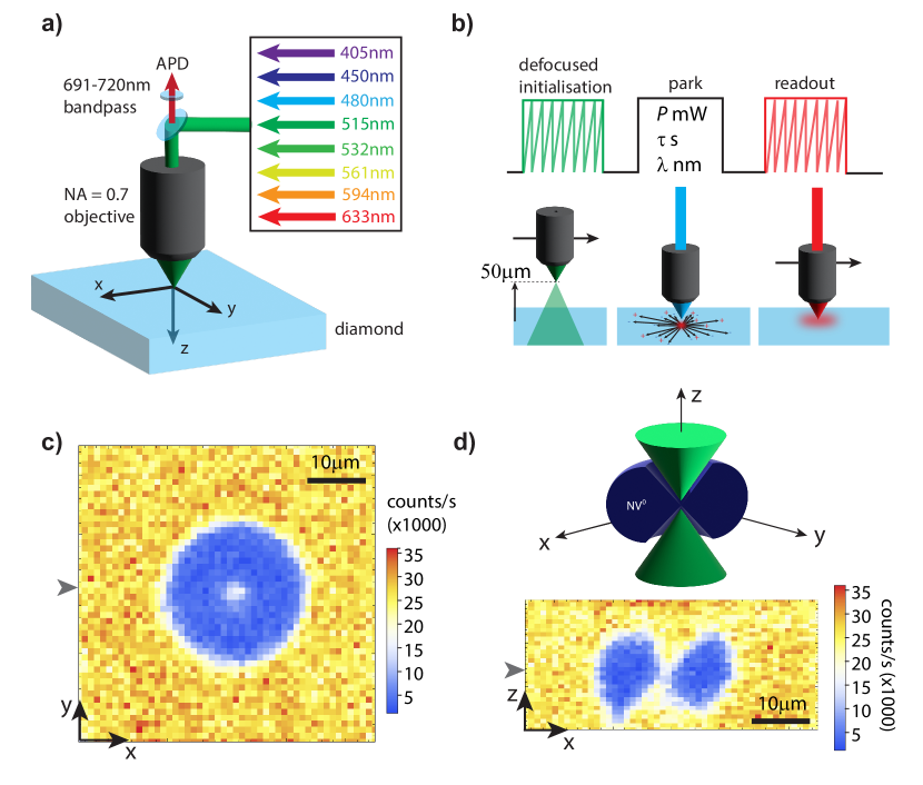
Our experimental procedure, shown in Fig. 1(b) follows three steps: initialization of defects into a particular charge state by scanning the optical illumination across a region of the diamond, followed by parking the illumination point at a fixed position with excitation wavelength , power for duration , and then finally a readout scanning step with weak red light (633 nm, 50 W) to read out the spatial charge distribution.
Charge initialization. Scanning green light over a given spatial region at set intensities initializes that region into a given defect charge state concentration. Immediately under the laser spot, green illumination favors the production of NV-. However at higher green powers, rapid generation of holes under the illumination spot from NV charge cycling [39] creates a halo-like region surrounding the laser spot of NV0 due to hole capture, as shown in Fig. 1(c). As the laser is scanned in position, it leaves a predominantly NV0 distribution in its wake. Thus, strong green scans prepare an NV0-rich, optically-dark region.
By elevating the microscope objective some m above the diamond surface during green illumination scans we create a large, low intensity illumination spot with negligible charge carrier generation compared to a tightly focused beam in the imaging plane. This ‘defocused preparation’ step is observed to maximize NV- generation, which we attribute to sufficiently low intensities to photoionize N0 () without instigating charge cycling of the NVs (). With continual photoionization of N0, free electrons are trapped by NV0 after sufficiently long illumination times (1-2 s). Scanning the laser beam broadens the effective preparation region, resulting in a bright, NV- rich preparation.
For sample B, containing a significant SiV fraction, strong green scans generate SiV- [9], while the defocused preparation step is observed to favor production of a NV- and SiV2- rich charge distribution, possibly via similar association of extra electrons to SiV-. The formation of SiV2- can also be attributed to the green photon energy (2.33 eV) exceeding the ionization threshold of SiV- (2.1 eV) [40, 41], and since NV charge cycling is minimized during defocused scanning, no process exists to generate holes to recombine to form SiV-. Similarly, strong green scanning in the imaging plane generates holes that deplete NV- and produce SiV-.
Scanning the laser beam position allows us to prepare regions of up to in a given charge state distribution. A single initialization step consists of a strong (8 mW) green scan followed by a defocused preparation, at 8 mW but with the objective m above the diamond surface.
Parking. Following initialization, we then apply a single laser pulse at a fixed location to induce local charge state conversion and the generation of free carriers. The parking step typically generates a dark charge-carrier capture pattern (CCP), or ‘halo’, around the illumination region as fluorescent defects (NV-) capture holes and transition to non-fluorescent charge states. Fig. 1(c) shows the salient features of these patterns formed under green illumination and imaged on a bright NV- background. Later in Section III, we will principally focus on the radius of this halo feature to quantitatively assess the rate of charge photogeneration. In previous work, charge carrier generation under green (532 nm and 514 nm) and red (633 nm) has been studied [42, 43, 31, 33], with the latter excitation wavelength suspected to induce charge cycling of either an unknown defect [32] or of SiV centers [10]. In this work, we study charge generation and capture using several key additional illumination wavelengths for the first time. Blue light (405-480 nm) induces single-photon mediated ionization and recombination for both NV- and NV0 [44] and subsequent charge cycling. Light at 561 nm is believed to excite NV charge cycling though without photoionization of nitrogen impurities [27], and 594 nm orange light is below the zero-phonon line excitation threshold for NV0 (575 nm), and as such should impair photorecombination of NV0 back to NV-, significantly altering NV charge cycling.
Readout. In all experiments described in this work, we read out the charge distribution pattern arising from a laser parking step with a weak red scan, typically W. At these powers, the intensity of the red light is low enough to prevent significant ionization of NV centers (NV) though still high enough to excite fluorescence. We limit the collected fluorescence to only NV- (691-730 nm), excluding SiV- emission (738 nm) and resulting in very high contrast between NV- (0.5-1 counts/s) and NV0 ( counts/s). Parking the green laser on Sample B generates a bright SiV- CCP with an inner dark region due to SiV0 [9, 10]. However, for direct comparison with Sample A, which exhibits no SiV fluorescence, we study only the NV charge populations.
The three-axis scanning capability of our microscope enables visualization of the depth () dependence of the CCP. In Figure 1(d), we present an - scan of the pattern, which appears to show lobes either side of the illumination region. This apparent asymmetry between - and - profiles of charge carrier photogeneration is a consequence of the axial expansion of the green laser exciting the NV centers. At the beam waist, the intensity is sufficient to excite photogeneration. However, the rapid expansion of the beam along the -axis results in a green intensity sufficient to only optically prepare NV- a few microns above the waist, resulting in a ‘punctured-sphere’ fluorescence distribution as depicted in the upper panel of Fig. 1(d).
III Wavelength dependence of photogeneration
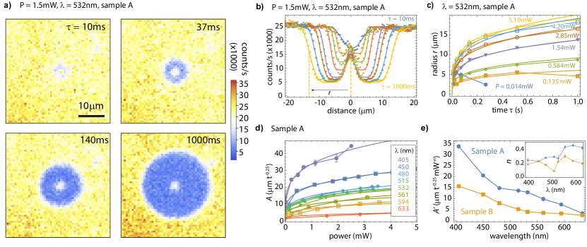
With our experimental procedure now fully described, we turn to an examination of the wavelength dependence of the charge carrier photogeneration process responsible for NV0 generation. In lieu of a high-power tunable laser source spanning the blue to near-IR, we select here several key illumination wavelengths easily sourced from commercial laser diodes or diode-pumped solid state systems. To parametrize the rate of charge carrier photogeneration, we consider as our figure of merit the radius of the NV0 region, and study how this radius increases as a function of time, power and wavelength. Figure 2(a) shows example confocal scans of NV0 generation following a mW, nm park for varied time. We consider an averaged 1D-lineout of the pattern and fit a function of the form to extract , the characteristic radius, as shown in Fig. 2(b). The double-quartic-gaussian function is chosen empirically due to the flat-bottomed profile of the halo patterns and the bright central maximum, which originates from NVs directly under the illumination spot. We then plot vs. for a selection of powers in Fig. 2(c).
The expansion of the radius as a function of time for all powers is observed to follow a -like dependence. A fit to the data of the form with free reveals little to no significant trend or variation in across the entire dataset of powers, wavelengths and both samples, consistent with the same underlying processes generating the halo pattern (i.e. charge generation, diffusion and capture but at different rates) so we fix and concentrate on the parameter . In Figure 2(d), we plot as a function of power for each excitation wavelength . We observe a clear trend towards rapid generation of large halos as the excitation energy increases, consistent with the photon energy exceeding the ground-state, single-photon ionization thresholds for both NV- and NV0, that is, between 2.74 and 2.78 eV (450 nm).
The parameter informs the size of a halo at a given time and power. The data in Fig. 2(d) is observed to follow a similar power law scaling as a function of optical power. Encapsulating the wavelength dependence into a single parameter which we term the ‘activity’, so that , we fit to the data in Fig. 2(d) and extract and as a function of wavelength. Fig. 2(e) (inset) shows the extracted activity () as a function of wavelength, for both ensemble-density samples considered in this work: sample A (nitrogen and NV only) and sample B (SiV, NV and nitrogen). For sample A we observe to vary from at 633 nm to at 405 nm, while for sample B remains nearly constant at . Sample B, which has an overall higher defect concentration in addition to the presence of SiV centers admits smaller charge generation halos. This is consistent with an increased trap density (NV- and SiV2- for holes, N+ for electrons) limiting the growth of the CCP, rather than any different charge generation processes (i.e. charge cycling of the SiV, which would be expected to result in larger CCP generation).
From energetic considerations, we can determine three regimes spanned by the illumination energies used in this work. For nm (2.76 eV), ionization and recombination between NV charge states is mediated by single photon transitions from the defect’s ground state. For nm (2.16 - 2.75 eV), the excitation energy is sufficient to allow two-photon ionization and recombination processes, with the limit of nm set by the ZPL of NV0. This energy lower limit stems from the necessity to first excite the NV0 transition [45], which promotes an electron to the state in the band gap, in so doing freeing a low-lying orbital in the band gap. Excitation of a valence electron to fill the band gap state is possible with photon energies as low as 1.2 eV [46], completing the two-step process of photorecombination back to NV-. For nm, the charge cycling process is not clear due to the insufficient photon energy to first excite NV0. We now study this observation more closely.
IV Red charge cycling: phonon-assisted anti-Stokes driving
With the observation that both orange (594 nm) and red (633 nm) light excites charge carrier generation in both SiV-rich and -poor samples, we conclude SiV centers play little if any role in cyclic carrier generation. Indeed, in the SiV-rich sample (B) the observed charge patterns are generally smaller and slower growing than in the NV-only sample (A). We therefore turn to the NV and nitrogen defects for an explanation. While carrier generation due to NV charge cycling is a reasonably well established process, the role of the substitutional nitrogen is not fully understood. For example, photoelectric measurements [44] and earlier bulk photoconductivity measurements [47, 48] report a large background photocurrent assumed to originate from the nitrogen defects. While neutral nitrogen (N0) occupies a donor level eV (730 nm) below the conduction band, the photoionization threshold has been measured to be closer to 2.2 eV [47] due to the significant energy cost associated with rearranging the nitrogen and carbon atoms upon removal of the electron. While photoionization with red light is thus inefficient, this process generates only electrons, not holes, from NN+, and direct photorecombination of NN0 is forbidden due to the eV acceptor level [49].
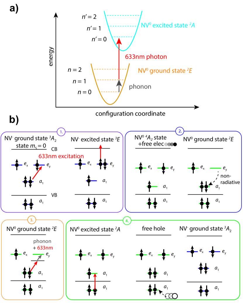
We therefore consider red-induced charge cycling of the NV directly, and posit phonon-assisted anti-Stokes excitation of the NV0 transition as the cause. A schematic of the anti-Stokes process and charge cycling is depicted in Fig. 3(a,b). In this process, a photon with insufficient energy (i.e. 633 nm, 1.96 eV) to directly excite an optical transition (the NV0 ZPL, 2.16 eV) is assisted by absorption of a phonon with sufficient energy to make up the difference in energy eV. Anti-Stokes excitation has been previously demonstrated for various color centers in wide band gap semiconductors [51]. For diamond, specific pertinent examples being 720 nm excitation of NV- (eV) [52], 780 nm excitation of SiV centers (eV) [53] (ZPL at 738 nm) and recently for 594 nm excitation of NV0 centers (eV) [54]. Indeed, recent work examining wavelength-dependence of both photocurrent and photoelectrically-detected magnetic resonance (PDMR) measures both photocurrent and PDMR contrast persisting between 575 nm and 637 nm (where it terminates [29]), further evidence of NV charge cycling under red excitation.
Two-photon ionization of NV- under red excitation is a well-understood process [6]. However, recent work has questioned the electronic state of NV0 immediately following ionization of NV- [50] and the consequences for charge cycling have not been fully discussed to date. The process depicted in Fig. 3(b) labeled (2) ascribes generation of NV0 in the ground state to non-radiative relaxation of the spin-quartet state that exists immediately following ionization, according to Ref. [50]. Previous works had suggested an Auger process was required to repopulate the intra-band state following ionization from the state [55, 26]. The post-ionization dynamics of the state were not considered in Ref. [50], and while described as metastable, the expected lifetime is of order 1 s [56], making charge cycling slower but not exceptionally so. In principle, direct optical excitation of the valence band state to the state in the band gap could potentially occur during the time spent in the state, which skips the non-radiative relaxation step. While possible, this process cannot be the only means of charge cycling, as it requires an initial state every time of NV- for charge cycling to proceed. We see charge cycling proceed regardless of initialization into NV- or NV0, with the latter assumed to be the equilibrium ground state of .
V Modeling charge generation and capture
For further understanding of the excitation wavelength dependence of charge carrier generation, we turn to a simulation of carrier generation and capture modeled by a system of equations that describe the time of evolution of hole, electron, NV centers and substitutional N concentrations in the presence of optical excitation [30, 9]. Briefly, these equations track the time and space-dependent populations of NV and subsitutional nitrogen, with optically-generated electrons and holes assumed to follow a diffusive spatial expansion upon creation followed by capture by surrounding defects. More details are provided in Appendix A.
Given a hole generation rate and uniform NV- density , one would simplistically assume that the radius of the CCP would increase with time as , that is, the time required to fill a sphere of radius . However, the scaling with optical power is not so easily extracted, and in any case the observed temporal dependence () deviates from this simple estimation. We were thus motivated to pursue a more in-depth analysis of carrier generation, diffusion and capture, not just of the NV centers but also the substitutional nitrogen, which has a strong effect on the diffusion of the carriers.
We assume that the wavelength-dependent electron generation rate (ionization) and hole generation rate (recombination) are related to the optical power by
| (1) |
with the subscripts denoting quadratic and linear terms and the gaussian beam waist of the focused laser. For simplicity we focus only on Sample A, which contains only NV and N and ignore electron generation from ionization of N0 and electron capture by NV0, though we do include hole capture by N0 as it is needed to fit the data. We assume radial symmetry, enabling the problem to be numerically solved one-dimensionally. We then vary the parameters and to best fit the CCP radius-vs-power data presented in Fig. 2(d) for Sample A.
We obtain excellent correspondence between the theoretical and experimental results. For 405 nm, both recombination and ionization are dominated by the one-photon processes, whereas in case of 532 nm illumination, solely the two-photon processes are sufficient to reproduce the data, as expected from the single NV experiments. Our particular interest lies in understanding how the CCP grows as a function of power, given the power dependence offers insight into the underlying optical charge cycling mechanism. Our calculation results are presented in Fig. 4. We define the characteristic diameter from a numerically-calculated CCP in an analogous manner to that used in experiments, as shown in Fig. 4(a). We then show the fitted power dependence at fixed illumination times for three key excitation wavelengths, 405 nm (ms), 532 nm (s) and 633 nm () in Fig. 4(b-d).
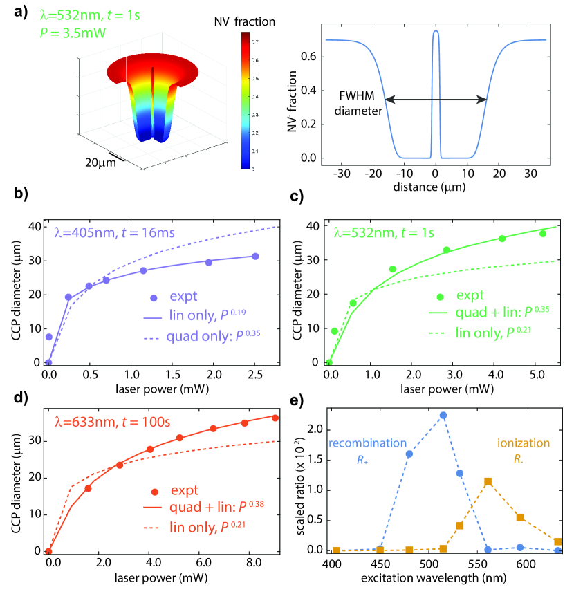
We are able to reproduce the characteristic temporal and power dependence characteristic of the expansion of the CCP, and also find that as expected, explicit consideration of a mixture of one-photon (nm, ) and two-photon processes (=2) are key to accurately reproducing the experimental data. This latter point is best illustrated by the dashed lines in Fig. 4(b-d), which are the fits including only two-photon power scaling (in the case of 405 nm) and one-photon scaling (for 532 nm and 633 nm). Importantly, the growth of the charge capture halo for nm is characteristic of a two-photon process, consistent with our hypothesis of anti-Stokes absorption mediating recombination of NV0. Finally, we compare quadratic to linear ionization and recombination rates using the figure of merit
| (2) |
defined so that when then , while for then , essentially quantifying when two-photon processes dominate over single-photon. We then calculate from extracted rates from numerical fits for each excitation wavelength and plot in Fig. 4(e). Here, we see distinct profiles corresponding roughly to the absorption profiles of NV0 (recombination) and NV- (ionization), evidence again of the underlying optical excitation processes driving CCP formation. These results offer an alternative to single-defect [6] or photocurrent [29] spectroscopy to probe the optical dependence of charge carrier generation, and ultimately the level structure of unknown defects that charge cycle under optical excitation.
VI Charge transfer between single NVs
To further corroborate our assertion that the NV center charge cycles slowly under red light, we turn to a third diamond (sample C) containing individually resolvable single NV centers. The sample has a low (ppb) nitrogen concentration and sparse distribution of NV centers, approximately 10 single NV centers within a , 10 m-thick region of isotopically-enriched 12C (0.2 %), with a surface. For these measurements, we switch to a second confocal microscope optimized for single-emitter detection, featuring an NA = 1.4 oil objective lens in an otherwise equivalent experimental configuration as described earlier. We identified two single NV centers (the ‘source’, which will be illuminated by red light, and ‘target’, which captures holes emitted from the source) separated by 4 m, as shown in Fig. 5(a), and implement the optical initialization and detection protocol depicted in Fig. 5(b). Here, a green scan initializes the target NV into NV- with approximately 70 fidelity, no green initialization is performed on the source NV. The position of the laser focus is then moved to the source NV, which is illuminated with red (633 nm) light with power for a duration , with defining a m radius arc where the red light position is varied, the source NV is located at . Following red pumping of the source, we move the laser focus back to the target and determine the charge state of the target with a 2 W scan of 594 nm light. With a photon energy below that of the NV0 ZPL, 594 nm orange light excites only NV- fluorescence for short illumination times, facilitating charge state detection [17]. A single orange light scan is insufficient to determine the charge state, so the whole sequence is repeated times to generate averaged images, shown in Fig. 5(c) for the case of a mW red laser pumping the target for varied times. The observed bleaching of NV- fluorescence is consistent with hole capture and formation of NV0, which appears dark due to the selection of optical filters [33].
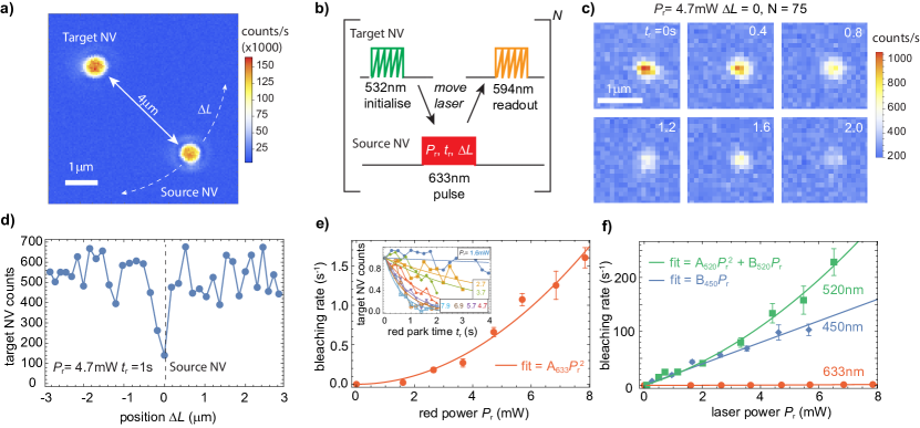
While commonly regarded as a sub-micron, diffraction-limited spot in the - imaging plane, the effective spatial extent of the illumination laser in our experiments is essentially a function of the power and illumination time. At high powers and illumination times approaching several seconds, the small fraction of power located in the Airy rings of the laser spot and various aberrations may result in direct bleaching of the target NV, even when the center of the beam is up to 2-3 m away [57]. We determined the effective width of the red laser beam by measuring the target NV bleaching as the laser was moved variable distances from the target along a line devoid of any NVs. For a 7 mW, 10 s exposure, m. Since the source NV is located m away, provided the product of laser powers and illumination times are kept less than mW s, the bleaching rate will not be affected by direct ionization of the target NV: the maximum we used in our measurements was 32 mW s.
To further verify that the source NV is indeed the source of holes, we then varied the position of the red laser along a 4m radius arc with length . In Figure 5(d), for a 4.7 mW, 1-s red pump on the source NV, we observed a narrow region centered on the position of the source NV () where bleaching of the target NV is maximal. This confirms the source NV is the origin of the charge carriers captured by the target NV. We then examined the dependence of target NV bleaching on red power applied to the source NV, as shown in Fig. 5(d). The target bleaching rate is observed to increase quadratically with red laser power, consistent with the hole generation at the source NV being mediated by a two-photon process.
To put the slow charge cycling of NVs under red light into context, we then considered an equivalent demonstration of much more rapid charge cycling using blue (450 nm) and green (520 nm) light. With an identical procedure as outlined before, we measured the power dependence of hole generation and capture between source and target for blue and green light, as shown in Fig. 5(e). For the same optical power, blue and green result in more than 100 faster hole generation. Indeed, for high blue or green excitation powers, hole capture by the target NV is detected within 1-5 ms, on the order of the NV spin-lattice relaxation time ms. Extension to magnetic-resonance based charge carrier detection is discussed further in Section VII.
The target-NV bleaching rates observed in this work are 10-20 faster than observed previously between single centers [33, 34]. Since the bleaching rate is a combination of the generation rate (strongly dependent on wavelength and the specifics of a given optical setup), carrier transport rate (sample dependent) and NV- capture cross-section (assumed to be independent of sample), direct comparison is not necessarily straightforward. However, a key difference between this work and previous work is the method of NV center incorporation. While both samples are CVD-grown, electronic grade material (sample C slightly isotopically depleted at 0.2 13C) and probed with similar experimental setups, the NV centers in our sample were incidentally incorporated during growth while those of Ref. [33, 34] created with high-energy (20 MeV) N+ ion implantation. We observed similarly fast hole capture rates in another sample (data not shown) with a slightly higher NV density, though it too was an as-grown sample without any subsequent treatment.
While hole generation and bleaching with blue light has a clear linear dependence with power , a combined linear and quadratic model is required to fully explain the power dependence of the 520 nm data . Such a linear-quadratic dependence was discernible in previous work [33] though not significantly outside experimental uncertainties. Recently, an increase of photocurrent production under illumination with 520 nm light was reported in NV ensembles [29] and attributed to a possible additional excited state of NV- in the conduction band, which may result in a more complicated, wavelength-dependent power dependence than a purely quadratic function. Regardless of additional excited states, the data in Fig. 2(e) would imply hole generation with blue should be much faster than that of 520 nm for the isolated single NVs. Here, we believe that imperfect aberration correction in the objective lens results in a slight position offset (notably in ) so that the laser spot size is not the same, nor in exactly the same position, for the two colors. Such an issue would not trouble our ensemble NV measurement, given the laser is always spatially overlapped with many NVs but can be severe for single NVs. NV0 fluorescence under 450 nm excitation could be resolved, though was observed to have significantly degraded -resolution. No NV fluorescence was observed under 405 nm excitation.
VII Discussion
In this work, we have examined how carrier photogeneration depends on illumination wavelength. Holes generated by NV charge cycling are captured by other NV-, and the size of the region of NV0 generated in a given time serves as a metric for the rate at which holes are generated. We studied diamonds with and without concentrations of silicon-vacancy centers, observing similar phenomenology that suggests SiV centers have a limited role in the generation of free holes in comparison to NV centers but affect the trasport of charge carriers through capture processes. At the very least, the contribution of NV centers to charge carrier generation under red illumination cannot be overlooked. We observe distinct regimes where differing mechanisms dominate the charge cycling rate, ranging from single-photon ionization for wavelengths nm, two-photon charge cycling for wavelengths between 450 and 561 nm, and a weaker process via which photon energies below the zero-phonon line energy of NV0 (2.15 eV, 575 nm) nevertheless manage to drive charge cycling (594 and 633 nm). We suggest anti-Stokes excitation of the NV0 transition as the process via which charge cycling is facilitated with red light. We confirm single NV centers charge cycle under red light this final regime by observing 633 nm-induced charge transfer between two isolated single NV centers.
The principal outcome of this work is the confirmation that the charge state of the NV center cycles under red light. Though weak and correspondingly slow, red charge cycling is on the timescale of typical NV experimental averaging times. Our work has important consequences for the identification of charge generation processes in photoelectric detection measurements [27, 29], where the excitation energy is one of the few means available of identifying what defects contribute to photocurrent generation and efforts to understand the charge interconversion of other defects, such as SiV centers [39, 58, 31]. This latter point is of particular importance, since precision measurement of ionization and recombination thresholds is an essential means of confirming the accuracy of theoretical models [41]. Future work could confirm the hypothesis of phonon-assisted, anti-Stokes mediated charge cycling by studying the temperature dependence of either carrier generation and capture or photocurrent generation.
An intriguing avenue of future inquiry concerns our final observation of rapid charge cycling and capture under blue and red light. For the highest powers used in these experiments, we could detect target NV hole capture and bleaching occurring in as little as 2 ms. Such an interval is well within the T1 time of the NVs we used and approaching the T2 time of NVs in highly-isotopically-enriched 12C diamond (ms). A future experiment could first initialize the target NV in the NV-, state before inducing optical charge cycling on the proximal source NV. Microwave pulses could then drive the target NV into a superposition state and enact a magnetometry protocol – such as a spin-echo sequence – to detect how proximal charges affect the coherence of the NV spin. Direct detection of diffusing charges may even be possible by employing an electron-electron resonance scheme where a second microwave field drives the spins of the diffusing charge carriers. Hole generation and capture are readily observed optically via charge conversion, but the electrons generated by NV charge cycling remain hidden, making their role in capture processes with nonfluorescent defects (eg N) unclear [13, 14]. Spin-based detection schemes could begin to shed new light on these processes, and make advances towards proposed schemes of quantum information distribution at room temperature in diamond [59]. Simple additions such as higher laser powers or closer NVs could bring spin-coherent sensing of carrier generation closer, though hardware limitations impose a limit on how fast the laser can be moved from one place to another. A potential solution exists in the recently developed dual-beam confocal microscopy developed to enable correlation sensing [60].
In conclusion, we have experimentally examined the wavelength dependence of optically-driven charge cycling of the NV center in diamond, observing single-photon and two-photon driven charge cycling and hole capture in both ensembles of NVs as well as individual single centers. We have demonstrated that red light induces slow but measurable charge cycling of the NV center, which is unexpected given the discrepancy between the red photon energy (1.95 eV) and NV0 ZPL (2.16 eV). We attribute this process to phonon-assisted anti-Stokes excitation of the NV0 ZPL. With green and blue induced charge cycling of a single NV, we were able to demonstrate 100 faster charge cycling and single-center hole capture than under red light, and faster than reported previously, enabling carrier transport and capture within the time of each center. Our work will be important for the identification and characterization of defect charge states in diamond, photoelectric measurement of the NV center and could open the way to coherent spin-based measurements of carrier transport in a room-temperature, wide band-gap semiconductor.
VIII Acknowledgments
This work was supported by the Australian Research Council (DE210101093). R. M. G. was supported by an Australian Governement Research Training Program (RTP) Scholarship. A.L. acknowledges support from the National Science Foundation under grant NSF-2216838. C.A.M. acknowledges support by the U.S. Department of Energy, Office of Science, National Quantum Information Science Research Centers, Co-design Center for Quantum Advantage (C2QA) under contract number DE-SC0012704. A.L. and C.A.M. acknowledge access to the facilities and research infrastructure of NSF CREST-IDEALS, grant number NSF-HRD-1547830.
Appendix A
Carrier diffusion simulation details. We model the formation of halos upon photogeneration of charge carriers through a system of diffusion equations that describe the time and space evolution of NV- population , positively-charged substitutional nitrogen N+ population , electron density and hole density . The equations are defined by admitting select processes that allow interconversion of NV and N charge states, which in turn generate electrons and holes that undergo diffusive transport, and may then be captured by more defects:
| (3) |
with as defined in Eq. 1, the total volume concentration of NV (NV0 and NV-), the total volume concentration of N (N0 and N+), s and s the electron and hole diffusion coefficients in diamond [30], and the coefficients representing probability of the capture of carrier by defect , proportional to the cross-section for the given process and the carrier velocity: s and [30].
We assume that since the NV can charge cycle indefinitely under laser illumination, it is the source of all free carriers and ignore photoionization of the N0 population. We used an NV concentration close to the value expected for the sample used for this work (10 ppb), however the value used for N (3.4 ppm) is higher than the 1 ppm anticipated for Sample A. This was done to account for an unknown number of hole and electron traps – beyond NV and N – present in a crystal that significantly affect the halo growth.
References
- Doherty et al. [2013] M. W. Doherty, N. B. Manson, P. Delaney, F. Jelezko, J. Wrachtrup, and L. C. L. Hollenberg, The nitrogen-vacancy colour centre in diamond, Physics Reports, 528, 1 (2013) .
- Thiering and Gali [2020] G. Thiering and A. Gali, Color centers in diamond for quantum applications, in Semiconductors and Semimetals, Diamond for Quantum Applications Part 1, Vol. 103, pp. 1–36, eds. C. E. Nebel, I. Aharonovich, N. Mizuochi, and M. Hatano (Elsevier, 2020).
- Castelletto and Boretti [2020] S. Castelletto and A. Boretti, Silicon carbide color centers for quantum applications, J. Phys. Photonics 2, 022001 (2020).
- Tran et al. [2016] T. T. Tran, C. Elbadawi, D. Totonjian, C. J. Lobo, G. Grosso, H. Moon, D. R. Englund, M. J. Ford, I. Aharonovich, and M. Toth, Robust Multicolor Single Photon Emission from Point Defects in Hexagonal Boron Nitride, ACS Nano 10, 7331 (2016).
- Caldwell et al. [2019] J. D. Caldwell, I. Aharonovich, G. Cassabois, J. H. Edgar, B. Gil, and D. N. Basov, Photonics with hexagonal boron nitride, Nat. Rev. Mater. 4, 552 (2019).
- Aslam et al. [2013] N. Aslam, G. Waldherr, P. Neumann, F. Jelezko, and J. Wrachtrup, Photo-induced ionization dynamics of the nitrogen vacancy defect in diamond investigated by single-shot charge state detection, New J. Phys. 15, 013064 (2013).
- Waldherr et al. [2011] G. Waldherr, J. Beck, M. Steiner, P. Neumann, A. Gali, T. Frauenheim, F. Jelezko, and J. Wrachtrup, Dark States of Single Nitrogen-Vacancy Centers in Diamond Unraveled by Single Shot NMR, Phys. Rev. Lett. 106, 157601 (2011).
- Rose et al. [2018] B. C. Rose, D. Huang, Z.-H. Zhang, P. Stevenson, A. M. Tyryshkin, S. Sangtawesin, S. Srinivasan, L. Loudin, M. L. Markham, A. M. Edmonds, D. J. Twitchen, S. A. Lyon, and N. P. de Leon, Observation of an environmentally insensitive solid-state spin defect in diamond, Science 361, 60 (2018).
- Wood et al. [2023] A. Wood, A. Lozovoi, Z.-H. Zhang, S. Sharma, G. I. López-Morales, H. Jayakumar, N. P. de Leon, and C. A. Meriles, Room-Temperature Photochromism of Silicon Vacancy Centers in CVD Diamond, Nano Lett. 23, 1017 (2023).
- Zhang et al. [2023] Z.-H. Zhang, A. M. Edmonds, N. Palmer, M. L. Markham, and N. P. de Leon, Neutral Silicon-Vacancy Centers in Diamond via Photoactivated Itinerant Carriers, Phys. Rev. Appl. 19, 034022 (2023).
- Ashfold et al. [2020] M. N. R. Ashfold, J. P. Goss, B. L. Green, P. W. May, M. E. Newton, and C. V. Peaker, Nitrogen in Diamond, Chem. Rev. 120, 5745 (2020).
- Manson et al. [2018] N. B. Manson, M. Hedges, M. S, J. Barson, R. Ahlefeldt, M. W. Doherty, M. J. Sellars, H. Abe, and T. Ohshima, NV- - N+ pair centre in 1b diamond, New J. Phys. 20, 113037 (2018).
- Lozovoi et al. [2020a] A. Lozovoi, D. Daw, H. Jayakumar, and C. A. Meriles, Dark defect charge dynamics in bulk chemical-vapor-deposition-grown diamonds probed via nitrogen vacancy centers, Phys. Rev. Materials 4, 053602 (2020a).
- Wang et al. [2023] G. Wang, C. Li, H. Tang, B. Li, F. Madonini, F. F. Alsallom, W. K. C. Sun, P. Peng, F. Villa, J. Li, and P. Cappellaro, Manipulating solid-state spin concentration through charge transportarXiv:2302.12742(2023) .
- Barry et al. [2020] J. F. Barry, J. M. Schloss, E. Bauch, M. J. Turner, C. A. Hart, L. M. Pham, and R. L. Walsworth, Sensitivity optimization for NV-diamond magnetometry, Rev. Mod. Phys. 92, 015004 (2020).
- Han et al. [2010] K. Y. Han, S. K. Kim, C. Eggeling, and S. W. Hell, Metastable Dark States Enable Ground State Depletion Microscopy of Nitrogen Vacancy Centers in Diamond with Diffraction-Unlimited Resolution, Nano Lett. 10, 3199 (2010).
- Shields et al. [2015] B. Shields, Q. Unterreithmeier, N. de Leon, H. Park, and M. Lukin, Efficient Readout of a Single Spin State in Diamond via Spin-to-Charge Conversion, Phys. Rev. Lett. 114, 136402 (2015).
- Dhomkar et al. [2016] S. Dhomkar, J. Henshaw, H. Jayakumar, and C. A. Meriles, Long-term data storage in diamond, Sci. Adv. 2, e1600911 (2016).
- Pfender et al. [2017] M. Pfender, N. Aslam, P. Simon, D. Antonov, G. Thiering, S. Burk, F. Fávaro de Oliveira, A. Denisenko, H. Fedder, J. Meijer, J. A. Garrido, A. Gali, T. Teraji, J. Isoya, M. W. Doherty, A. Alkauskas, A. Gallo, A. Grüneis, P. Neumann, and J. Wrachtrup, Protecting a Diamond Quantum Memory by Charge State Control, Nano Lett. 17, 5931 (2017).
- McCloskey et al. [2022] D. J. McCloskey, N. Dontschuk, A. Stacey, C. Pattinson, A. Nadarajah, L. T. Hall, L. C. L. Hollenberg, S. Prawer, and D. A. Simpson, A diamond voltage imaging microscope, Nat. Photon. 16, 730 (2022).
- Monge et al. [2023] R. Monge, T. Delord, and C. A. Meriles, Reversible optical data storage below the diffraction limit, Nat. Nanotechnol. , 1 (2023).
- Ji et al. [2024] W. Ji, Z. Liu, Y. Guo, Z. Hu, J. Zhou, S. Dai, Y. Chen, P. Yu, M. Wang, K. Xia, F. Shi, Y. Wang, and J. Du, Correlated sensing with a solid-state quantum multisensor system for atomic-scale structural analysis, Nat. Photon. , 1 (2024).
- Delord et al. [2024] T. Delord, R. Monge, and C. A.,Correlated spectroscopy of electric noise with color center clusters Meriles, arXiv:2401.07814 (2024) .
- Bourgeois et al. [2015] E. Bourgeois, A. Jarmola, P. Siyushev, M. Gulka, J. Hruby, F. Jelezko, D. Budker, and M. Nesladek, Photoelectric detection of electron spin resonance of nitrogen-vacancy centres in diamond, Nat. Commun. 6, 8577 (2015).
- Siyushev et al. [2019] P. Siyushev, M. Nesladek, E. Bourgeois, M. Gulka, J. Hruby, T. Yamamoto, M. Trupke, T. Teraji, J. Isoya, and F. Jelezko, Photoelectrical imaging and coherent spin-state readout of single nitrogen-vacancy centers in diamond, Science 363, 728 (2019).
- Bourgeois et al. [2020] E. Bourgeois, M. Gulka, and M. Nesladek, Photoelectric Detection and Quantum Readout of Nitrogen-Vacancy Center Spin States in Diamond, Adv. Opt. Mat. 8, 1902132 (2020).
- Hruby et al. [2022] J. Hruby, M. Gulka, M. Mongillo, I. P. Radu, M. V. Petrov, E. Bourgeois, and M. Nesladek, Magnetic field sensitivity of the photoelectrically read nitrogen-vacancy centers in diamond, Appl. Phys. Lett. 120, 162402 (2022).
- Bourgeois et al. [2022] E. Bourgeois, J. Soucek, J. Hruby, M. Gulka, and M. Nesladek, Photoelectric Detection of Nitrogen-Vacancy Centers Magnetic Resonances in Diamond: Role of Charge Exchanges with Other Optoelectrically Active Defects, Adv. Quantum Technol. 5, 2100153 (2022).
- Todenhagen and Brandt [2023] L. M. Todenhagen and M. S. Brandt, Wavelength Dependence of the Electrical and Optical Readout of NV Centers in Diamond, arXiv:2307.11830 (2023) .
- Lozovoi et al. [2020b] A. Lozovoi, H. Jayakumar, D. Daw, A. Lakra, and C. A. Meriles, Probing Metastable Space-Charge Potentials in a Wide Band Gap Semiconductor, Phys. Rev. Lett. 125, 256602 (2020b).
- Gardill et al. [2021] A. Gardill, I. Kemeny, M. C. Cambria, Y. Li, H. T. Dinani, A. Norambuena, J. R. Maze, V. Lordi, and S. Kolkowitz, Probing Charge Dynamics in Diamond with an Individual Color Center, Nano Lett. 21, 6960 (2021).
- Lozovoi et al. [2022] A. Lozovoi, G. Vizkelethy, E. Bielejec, and C. A. Meriles, Imaging dark charge emitters in diamond via carrier-to-photon conversion, Science Advances 8, eabl9402 (2022).
- Lozovoi et al. [2021] A. Lozovoi, H. Jayakumar, D. Daw, G. Vizkelethy, E. Bielejec, M. W. Doherty, J. Flick, and C. A. Meriles, Optical activation and detection of charge transport between individual colour centres in diamond, Nat Electron 4, 717 (2021).
- Lozovoi et al. [2023] A. Lozovoi, Y. Chen, G. Vizkelethy, E. Bielejec, J. Flick, M. W. Doherty, and C. A. Meriles, Detection and Modeling of Hole Capture by Single Point Defects under Variable Electric Fields, Nano Lett. 23, 4495 (2023).
- Zheng et al. [2022] W. Zheng, K. Bian, X. Chen, Y. Shen, S. Zhang, R. Stöhr, A. Denisenko, J. Wrachtrup, S. Yang, and Y. Jiang, Coherence enhancement of solid-state qubits by local manipulation of the electron spin bath, Nat. Phys. 18, 1317 (2022).
- Görlitz et al. [2022] J. Görlitz, D. Herrmann, P. Fuchs, T. Iwasaki, T. Taniguchi, D. Rogalla, D. Hardeman, P.-O. Colard, M. Markham, M. Hatano, and C. Becher, Coherence of a charge stabilised tin-vacancy spin in diamond, npj Quantum Inf 8, 1 (2022).
- Zuber et al. [2023] J. A. Zuber, M. Li, M. l. G. Puigibert, J. Happacher, P. Reiser, B. J. Shields, and P. Maletinsky, Shallow Silicon Vacancy Centers with lifetime-limited optical linewidths in Diamond Nanostructures, arXiv:2307.12753 (2023) .
- Edmonds et al. [2012] A. M. Edmonds, U. F. S. D’Haenens-Johansson, R. J. Cruddace, M. E. Newton, K.-M. C. Fu, C. Santori, R. G. Beausoleil, D. J. Twitchen, and M. L. Markham, Production of oriented nitrogen-vacancy color centers in synthetic diamond, Phys. Rev. B 86, 035201 (2012).
- Dhomkar et al. [2018] S. Dhomkar, P. R. Zangara, J. Henshaw, and C. A. Meriles, On-Demand Generation of Neutral and Negatively Charged Silicon-Vacancy Centers in Diamond, Phys. Rev. Lett. 120, 117401 (2018).
- Gali and Maze [2013] A. Gali and J. R. Maze, Ab initio study of the split silicon-vacancy defect in diamond: Electronic structure and related properties, Phys. Rev. B 88, 235205 (2013).
- Thiering and Gali [2018] G. Thiering and A. Gali, Ab Initio Magneto-Optical Spectrum of Group-IV Vacancy Color Centers in Diamond, Phys. Rev. X 8, 021063 (2018).
- Jayakumar et al. [2016] H. Jayakumar, J. Henshaw, S. Dhomkar, D. Pagliero, A. Laraoui, N. B. Manson, R. Albu, M. W. Doherty, and C. A. Meriles, Optical patterning of trapped charge in nitrogen-doped diamond, Nat Commun 7, 12660 (2016).
- Jayakumar et al. [2020] H. Jayakumar, A. Lozovoi, D. Daw, and C. Meriles, Long-Term Spin State Storage Using Ancilla Charge Memories, Phys. Rev. Lett. 125, 236601 (2020).
- Bourgeois et al. [2017] E. Bourgeois, E. Londero, K. Buczak, J. Hruby, M. Gulka, Y. Balasubramaniam, G. Wachter, J. Stursa, K. Dobes, F. Aumayr, M. Trupke, A. Gali, and M. Nesladek, Enhanced photoelectric detection of NV magnetic resonances in diamond under dual-beam excitation, Phys. Rev. B 95, 041402 (2017).
- Manson et al. [2013] N. B. Manson, K. Beha, A. Batalov, L. J. Rogers, M. W. Doherty, R. Bratschitsch, and A. Leitenstorfer, Assignment of the NV0 575-nm zero-phonon line in diamond to a - transition, Phys. Rev. B 87, 155209 (2013).
- Meirzada et al. [2018] I. Meirzada, Y. Hovav, S. A. Wolf, and N. Bar-Gill, Negative charge enhancement of near-surface nitrogen vacancy centers by multicolor excitation, Phys. Rev. B 98, 245411 (2018).
- Nesládek et al. [1998] M. Nesládek, L. M. Stals, A. Stesmans, K. Iakoubovskij, G. J. Adriaenssens, J. Rosa, and M. Vaněček, Dominant defect levels in diamond thin films: A photocurrent and electron paramagnetic resonance study, Applied Physics Letters 72, 3306 (1998).
- Rosa et al. [1999] J. Rosa, M. Vaněček, M. Nesládek, and L. M. Stals, Photoionization cross-section of dominant defects in CVD diamond, Diamond and Related Materials 8, 721 (1999).
- Jones et al. [2009] R. Jones, J. P. Goss, and P. R. Briddon, Acceptor level of nitrogen in diamond and the 270-nm absorption band, Phys. Rev. B 80, 033205 (2009).
- Razinkovas et al. [2021] L. Razinkovas, M. Maciaszek, F. Reinhard, M. W. Doherty, and A. Alkauskas, Photoionization of negatively charged NV centers in diamond: Theory and ab initio calculations, Phys. Rev. B 104, 235301 (2021).
- Lin et al. [2022] W.-X. Lin, J.-F. Wang, Q. Li, J.-Y. Zhou, J.-S. Xu, C.-F. Li, and G.-C. Guo, Anti-Stokes excitation of optically active point defects in semiconductor materials, Mater. Quantum. Technol. 2, 042001 (2022).
- Tran et al. [2019] T. T. Tran, B. Regan, E. A. Ekimov, Z. Mu, Y. Zhou, W.-b. Gao, P. Narang, A. S. Solntsev, M. Toth, I. Aharonovich, and C. Bradac, Anti-Stokes excitation of solid-state quantum emitters for nanoscale thermometry, Science Advances 5, eaav9180 (2019).
- Gao et al. [2018] Y.-F. Gao, Q.-H. Tan, X.-L. Liu, S.-L. Ren, Y.-J. Sun, D. Meng, Y.-J. Lu, P.-H. Tan, C.-X. Shan, and J. Zhang, Phonon-Assisted Photoluminescence Up-Conversion of Silicon-Vacancy Centers in Diamond, J. Phys. Chem. Lett. 9, 6656 (2018).
- Gao et al. [2022] Y.-F. Gao, J.-M. Lai, Y.-J. Sun, X.-L. Liu, C.-N. Lin, P.-H. Tan, C.-X. Shan, and J. Zhang, Charge State Manipulation of NV Centers in Diamond under Phonon-Assisted Anti-Stokes Excitation of NV0, ACS Photonics 9, 1605 (2022).
- Siyushev et al. [2013] P. Siyushev, H. Pinto, M. Vörös, A. Gali, F. Jelezko, and J. Wrachtrup, Optically Controlled Switching of the Charge State of a Single Nitrogen-Vacancy Center in Diamond at Cryogenic Temperatures, Phys. Rev. Lett. 110, 167402 (2013).
- Gali [2009] A. Gali, Theory of the neutral nitrogen-vacancy center in diamond and its application to the realization of a qubit, Phys. Rev. B 79, 235210 (2009).
- Gardill et al. [2022] A. Gardill, I. Kemeny, Y. Li, M. Zahedian, M. C. Cambria, X. Xu, V. Lordi, A. Gali, J. R. Maze, J. T. Choy, and S. Kolkowitz, Super-Resolution Airy Disk Microscopy of Individual Color Centers in Diamond, ACS Photonics 9, 3848 (2022).
- Nicolas et al. [2019] L. Nicolas, T. Delord, P. Huillery,C. Pellet-Mary, and G. Hétet, ACS Photonics 6, 2413-2420 (2019).
- Doherty et al. [2016] M. Doherty, C. Meriles, A. Alkauskas, H. Fedder, M. Sellars, and N. Manson, Towards a Room-Temperature Spin Quantum Bus in Diamond via Electron Photoionization, Transport, and Capture, Phys. Rev. X 6, 041035 (2016).
- Rovny et al. [2022] J. Rovny, Z. Yuan, M. Fitzpatrick, A. I. Abdalla, L. Futamura, C. Fox, M. C. Cambria, S. Kolkowitz, and N. P. de Leon, Nanoscale covariance magnetometry with diamond quantum sensors, Science 378, 1301 (2022).