Laser-induced quenching of metastability at the Mott-insulator to metal transition
Abstract
There is growing interest in strongly correlated insulator thin films because the intricate interplay of their intrinsic and extrinsic state variables causes memristive behavior that might be used for bio-mimetic devices in the emerging field of neuromorphic computing. In this study we find that laser irradiation tends to drive V2O3 from supercooled/superheated metastable states towards thermodynamic equilibrium, most likely in a non-thermal way. We study thin films of the prototypical Mott-insulator V2O3, which show spontaneous phase separation into metal-insulator herringbone domains during the Mott transition. Here, we use low-temperature microscopy to investigate how these metal-insulator domains can be modified by scanning a focused laser beam across the thin film surface. We find that the response depends on the thermal history: When the thin film is heated from below the Mott transition temperature, the laser beam predominantly induces metallic domains. On the contrary, when the thin film is cooled from a temperature above the transition, the laser beam predominantly induces insulating domains. Very likely, the V2O3 thin film is in a superheated or supercooled state, respectively, during the first-order phase transition, and the perturbation by a laser beam drives these metastable states into stable ones. This way, the thermal history is locally erased. Our findings are supported by a phenomenological model with a laser-induced lowering of the energy barrier between the metastable and equilibrium states.
Strongly correlated insulator thin films are the subject of intensive research in the emerging field of neuromorphic computing [3, 4, 5, 6]. If these materials are cooled to a temperature below the transition temperature, the charge carrier mobility is considerably reduced due to electron-electron correlation effects like the Mott-Hubbard interaction (e.g., V2O3 [7, 8, 9, 10, 11]), charge transfer (e.g., rare-earth nickelates [12, 13]) or dimerization (e.g., VO2)[14]. This reduction in charge carrier mobility results in a metal-to-insulator transition (MIT) [15]. An equivalent insulator-to-metal transition (IMT) is observed during heating. The electron-electron correlation effects cause an intricate interplay of intrinsic and extrinsic state variables that can be leveraged for engineering neuromorphic devices [16]. One way to influence strongly correlated insulator thin-film devices externally is through exposure to light. For instance, light is used to trigger resistive switching [17, 18, 19, 20], to tune the resistive switching voltage thresholds [21] or to tune the frequency of relaxation oscillators [22] in VO2 devices. Furthermore, because strongly correlated insulator thin-film neuromorphic devices are usually operated in a critical state at the onset of the IMT/MIT, their functionality is affected by thermodynamics of phase transitions. For instance, the hysteresis in resistance vs temperature curves due to the first order MIT/IMT in VO2 is leveraged for multistate resistive switching [23, 24, 25]. In V2O3, the MIT/IMT is accompanied by structural (corundum to monclinic) and magnetic (paramagnetic to antiferromagnetic) phase transitions, providing a complex interplay of many degrees of freedom [26, 27, 28, 29]. As a foundation of utilizing V2O3-based neuromorphic device applications that are implementing light as an external stimulus, one needs a better understanding of the phase transitions in V2O3.
We have investigated the effect of laser scanning irradiation on a V2O3 thin film during the IMT/MIT by acquiring photomicrographs. Here we report on laser-induced phase transitions. While at the IMT, the metal phase is induced, the insulating phase is predominantly induced at the MIT. The latter is surprising, because one might expect the main effect of the laser irradiation to be heating, which is expected to drive the system towards a more metallic state.
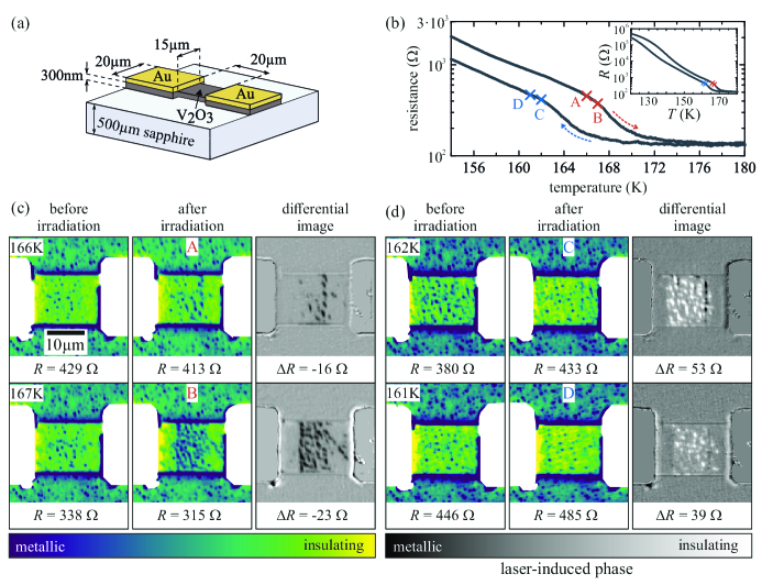
The sample under investigation is a continuous 300-nm-thick rf-sputtered V2O3 film on an r-cut sapphire substrate with gold electrodes evaporated on top (see Ref. [30] for details); Fig. 1(a) shows its curve for both heating and cooling. The resistance change of four orders of magnitude at the phase transition is a sign of high film quality.
We used the same optical microscopy setup as in Lange et al. [31], where we have demonstrated that the change in reflectivity allows for imaging the separation of the insulating and metallic phases with 0.5 m spatial resolution. As described in Refs. [32, 33], the setup is a cryogenic combined widefield and laser scanning microscope. A sketch of the experimental setup is shown in Fig. 1(b), and a detailed description is given in Ref. [34] (Sec. I).
For this study, the photomicrographs are acquired in the widefield mode with an monochromatic (532 nm) LED illumination, and the laser scanning mode is used for exposing the sample under investigation to laser light of 405 nm wavelength. The theoretical laser spot diameter on the thin-film surface is 322 nm. We have measured the incident laser power on the sample surface by replacing the sample with a photodiode. The maximum laser power is 919 W. However, different laser powers were chosen, throughout this study. For exposure, the selected area is scanned line by line (line separation 100 nm) with the laser in the continuous wave mode as depicted in Fig. 1(b). During each line scan, the laser spot stays at a position for 13 ms then it moves to the next position at a distance of 100 nm.
The procedure to investigate the effect of laser scanning irradiation is the following:
-
1.
A photomicrograph (3232 m2) of the thin film is acquired.
-
2.
A selected area (1414 m2) is exposed to laser light.
-
3.
A second photomicrograph is acquired.
-
4.
For the differential image, the first photomicrograph is subtracted from the second.
With this procedure, the laser-induced changes from the metallic to the insulating and from the insulating to the metallic phases are mapped.
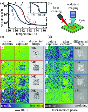
We have exposed a V2O3 thin film by laser light at different temperatures during the IMT/MIT (Fig. 1). The curve shows a hysteresis of several Kelvins due to the first-oder nature of the IMT/MIT [9]. During heating of the sample from 80 K to room temperature, the heating was interrupted four times during the IMT, and a pristine (unirradiated) 1414 m area was exposed with 0.1 mW laser power according to the procedure described above. The same procedure was chosen for cooling from room temperature to 80 K with 0.6 mW laser power. Note, that we chose different pristine areas on the sample for each scanning procedure. The photomicrographs in Fig. 1(c),(d) (in particular, D and E) show the characteristic herringbone domain pattern due to strain-induced separation of the metallic and insulating phases [35, 31]. A crucial result of this study is that during heating, mostly metallic domains are induced (dark patches in the differential images in Fig. 1(c) and (d)), whereas during cooling, predominantly insulating domains are created by laser irradiation (bright patches in the differential images in Fig. 1(c) and (d)). Furthermore, laser scanning irradiation does not smear or destroy the herringbone domain patterns but modifies them by changing the ratio of the metallic and insulating surface areas. In an additional experiment on a patterned V2O3 thin film microbridge (see Fig. S2 in Ref. [34]) we show, that indeed the laser-scanning-induced phase change has a significant effect on the film resistivity. Moreover, we observe that the size of the laser-induced domains is similar to the size of the domains of the temperature-driven phase transition without laser exposure. This indicates, that domain walls permeate the whole film, and that the laser-induced phase transition is not only due to a surface effect.
We also modified the laser irradiation procedure to determine the power thresholds for laser-induced phase changes during heating and cooling (see Sec. III in Ref. [34] for details). It was found that laser irradiation already at relatively low power levels induces a phase change during heating (i.e., IMT), while during cooling (i.e., MIT), the required laser power is considerably larger. Moreover, the temperature range, in which a laser-induced phase change was observable, is larger during IMT, compared to MIT. Hence, the heating branch of the transition seems to be more sensitive to laser irradiation than the cooling branch.
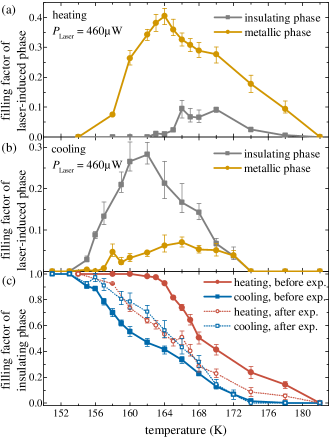
For a quantitative analysis of the laser-induced phase changes, we investigated the filling factors, i.e., the ratio between the surface area of a particular phase and the total surface area of interest at a laser power of 460 W. This laser power was chosen because it is far from the minimum and maximum threshold values for both cooling and heating (see Sec. III in Ref. [34]). As mentioned above, the metallic and insulating thin-film areas can be clearly distinguished by their brightness level in the photomicrographs (see Fig. 1 and [31]). However, these brightness levels change from micrograph to micrograph. Therefore, the following evaluation procedure was used for determining the filling factors. We visually inspected the (differential) micrographs in Fiji [36] and chose an upper and lower limit for the brightness that separates the particular two phases. A third brightness level was calculated by averaging the upper and lower limit. For these three brightness values, we calculated the filling factors, which correspond to the data points and the error bars in Fig. 2, using a Python routine.
Figure 2(a) and (b) show the temperature dependence of the filling factors of the laser-induced metallic and insulating phases during heating and cooling, respectively. Except for the fact that in the heating case, predominantly the metallic, and in the cooling case, predominantly the insulating phase is created, the overall behavior is very similar: the laser irradiation switches a considerable percentage of the thin-film area during the IMT from insulating to metallic (40% at 164 K) and during the MIT from metallic to insulating (28% at 162 K). Furthermore, in both cases, there is a temperature interval in which a smaller amount of the minor phase (insulating at the IMT and metallic at the MIT) is induced as well.
Figure 2(c) shows the filling factor of the insulating phase before and after laser irradiation. The error bars of the before-irradiation graphs are smaller compared to the after-irradiation graphs because a larger area was used for determining the filling factors before irradiation. Like the -curves shown in Fig. 1(a), the before-irradiation curves are hysteretic due to the first-order character of the IMT/MIT phase transitions. Most importantly, the after-irradiation curves (dashed lines) lay between the curves before irradiation and are almost identical for temperatures at 168 K and below (solid lines). This implies that after irradiation, it is no longer possible to decide (by means of the filling factor) whether the film was in the heating or cooling branch. In this sense, laser irradiation above the power threshold erases the thermal history of the V2O3 thin film.
The most intriguing result of this study is that laser irradiation predominantly induces insulating domains in large amounts during cooling. Considering the laser spot as a local heat source, it is not surprising that laser irradiation induces metallic domains since the metallic phase is the high-temperature phase of the Mott transition. Indeed, we observe this behavior during heating of the sample through the IMT. However, the predominant laser-induced creation of insulating domains during cooling is puzzling. In other words, why does the effect of laser irradiation depend on the thermal history? To answer this question, the thermodynamic nature of the MIT/IMT of the V2O3 thin film must be considered.
The thermodynamic description of V2O3 thin films is the subject of ongoing research [37, 38, 39]. It is recognized that at the MIT, three phase transitions are coupled: first, an electronic transition due to Mott-Hubbard charge carrier localization, second, a magnetic transition from a paramagnetic-to-antiferromagnetic state, and third, a structural transition from corundum to a monoclinic crystal structure. Furthermore, as indicated in Ref. [31], the characteristic herringbone domain pattern resembles the solutions of the Cahn-Larché equation describing a phase separation due to spinodal decomposition [40]. Other studies also indicate that the IMT/MIT is associated with a spinodal instability [41, 42]. Despite those intricate details, the -hysteresis and the associated latent heat at the IMT and MIT clearly indicate a first-order phase transition. Consequently, it is safe to assume that during heating the V2O3 thin film is in a metastable superheated state, and during cooling it is in a metastable supercooled state. The most likely interpretation of our results is that the perturbation releases the V2O3 thin film from its metastable state, and when the laser spot moves to a new position, the thin film relaxes locally into a stable state. The general details of the perturbation induced by the laser beam are elusive and additional effects might be at play, for instance, a photoinduced change of the 3-orbital occupation could trigger the formation of metallic nanodroplets in the IMT [43].
With respect to the MIT we measured electrical transport properties during minor thermal cycles to investigate how heating affects a V2O3 thin film in the critical state. This procedure emulates a heat source that changes the temperature gradually on a large length scale. A detailed description and discussion of these additional experiments can be found in Ref. [34] (Sec. IV). Although we found that a minor heating cycle can indeed increase the resistance, the effect is not strong enough to account for what we observed in the laser irradiation experiment.
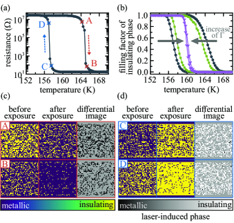
To elaborate on the matter of metastability, we discuss a phenomenological numerical model. In a two-dimensional (2D) resistor network, each site can either be metallic or insulating, depending on the local temperature, which is updated at every simulation step. Solving Kirchhoff’s laws, currents and voltages on each site are determined. A first-order Landau-type free energy functional provides stable and metastable states separated by a barrier. The laser irradiation is implemented in the model by decreasing the barrier height to drive transitions between insulating and metallic states. For each site, the escape from a metastable state was determined by comparing random numbers to Boltzmann factors with a constant number of iterations. If the escape criterion is fulfilled, the transition probability is given by a Boltzmann distribution; see Sec. V in Ref. [34] for details.
Our model reproduces the hysteresis in the curves, as shown in Fig. 3(a). Figure 3(b) shows the evolution of the filling factor of the insulating phase at different laser intensities. With increasing laser intensity the hysteresis is diminished, and eventually it is completely suppressed, similarly to the experimental results in Fig. 2(c). In Fig. 3(c) we present a simulation series of selected network maps before and after laser exposure with moderate laser intensity ( = 600 K), and their corresponding differential images. For heating, the laser induces predominantly metallic sites (Fig. 3(c)), for cooling insulating sites (Fig. 3(d)). We note that during heating, the majority of sites goes into a metallic state (indicated by black squares in the differential maps), while a few sites revert back to an insulating state (indicated by white squares in the differential maps); this reproduces very well the experimental results. Moreover, this behavior reverses in the cooling branch (Fig. 3(d), again in agreement with experimental observations. So, according to the simulations, the laser irradiation enhances the process of relaxing the system from a metastable state.
In conclusion, we can state that a V2O3 thin film in the metastable state at the IMT/MIT is highly susceptible to a local perturbation by a focused laser beam at the sub-micrometer scale. Whether the laser perturbation predominantly creates a metallic or insulating phase depends on whether the film is in the heating or cooling branch. Our observations tell that the laser beam brings the system from a supercooled/superheated state to the equilibrium one, provided that the laser power is sufficient to overcome corresponding energy barriers. This implies, that laser scanning irradiation can be used to effectively erase thermal history and provides a novel method to reset memristive devices locally. Our experiments may also be considered as a clear indication that external stimuli on a strongly correlated thin film in a critical state can result in unexpected and presumably non-thermal effects. Non-thermal effects have been investigated in ultra-fast pump-probe experiments on VO2 and V2O3 [44, 45, 46, 43, 47]. In contrast, in our experiment we have a quasi-static setting. The findings of this study may trigger additional experimental and theoretical studies to explore the thermodynamics of phase transitions and local perturbations in this class of materials.
Acknowledgements.
T.L. acknowledges support from the Cusanuswerk, Bischöfliche Studienförderung, F.T. acknowledges support from the Landesgraduiertenförderung Baden-Württemberg and M.R. acknowledges support from the French ANR “MoMA” project ANR-19-CE30-0020. This project has received funding from the European Union’s Horizon Europe research and innovation programme under grant agreement No. 2031928 – “Highly Energy-Efficient Resistive Switching in Defect- and Strain- Engineered Mott Insulators for Neuromorphic Computing Applications”. Views and opinions expressed are however those of the authors only and do not necessarily reflect those of the European union or the European research council. Work at University of California San Diego (UCSD) was supported through an Energy Frontier Research Center program funded by the US Department of Energy (DOE), Office of Science, Basic Energy Sciences, under Grant DE-SC0019273.References
- [1]
- [2]
References
I Sample and Measurement Setup
The sample under investigation (Fig. S1(a)) is a continuous 300-nm-thick rf-sputtered V2O3 film on an r-cut sapphire substrate. Using a shadow mask, four 2-mm-long parallel gold electrodes with a distance of 1.5 mm were evaporated as contacts for resistance measurements. The sample is mounted in vacuum on the coldfinger of a liquid Helium continuous-flow cryostat with a temperature range of 4.2 K to 300 K. Electric transport measurements were performed using a Keithley 2400 SourceMeter configured as a current source.
The experimental setup is a cryogenic combined widefield and laser scanning microscope, which is described in detail in [4, 5]. Figure S1(b) shows a simplified schematic of the microscope setup that can be operated either in the widefield or in the laser scanning mode.
The illumination for the widefield microscope is realized by a LED with 532 nm wavelength and follows a Köhler illumination scheme. The depicted field lens is used to define the illuminated sample area. After passing a beam splitter, the light is reflected by a removable mirror and is focused onto the sample by the microscope objective lens. The microscope objective has a high numerical aperture (NA = 0.8), which allows for a working distance of 1 mm. After reflection from the sample, the light travels the same way back, is deflected by the beam splitter and then focused onto the sensor of a low noise sCMOS camera. This widefield microscope has a field of view (FOV) of 500500 m2 and a spatial resolution of m. The entire optical path of the widefield microscope is polarization sensitive, which however is not relevant for this study.
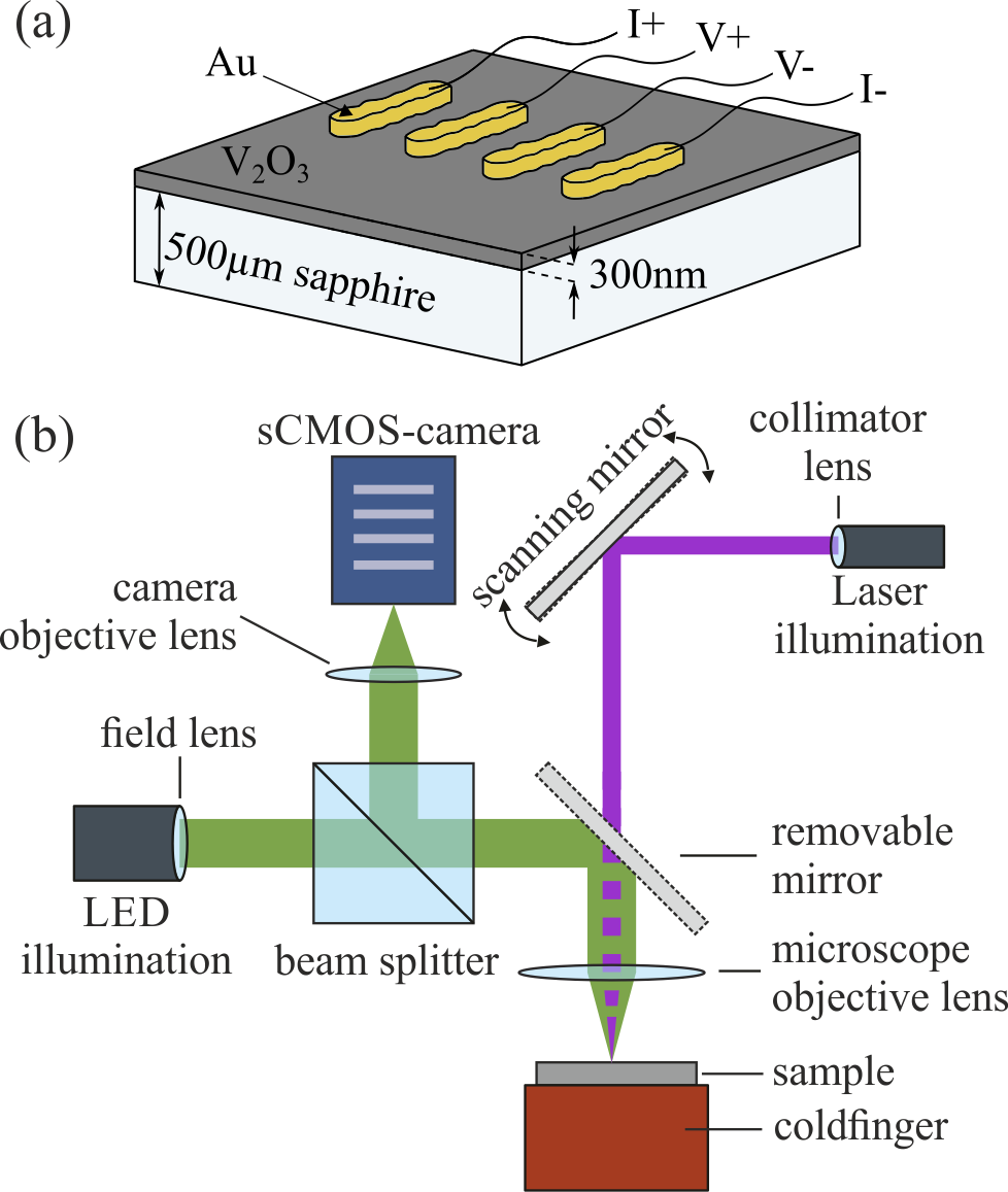
The illumination for the laser scanning microscope is provided by a 405-nm-laser diode coupled into a single mode fiber. The laser light is collimated and thereafter reflected by a fast steering mirror, that serves as scanning mirror. In order to use this operation mode, the removable mirror is not inserted in the beam path. The laser beam is focused onto the sample by the microscope objective lens. Assuming a Gaussian beam profile, the theoretical laser spot diameter is 322 nm (1/ diameter). The FOV of the laser scanning microscope is identical with the FOV of the widefield microscope. The polarization sensitive components and the detector unit of the laser light are not included here, because in this study, we use the laser scanning microscope exclusively for irradiation.
II Microbridge experiment
In order to confirm the hypothesis, that laser scanning indeed induces phase transitions, we investigated its effect on the electrical properties of a V2O3 microbridge device in an additional experiment. The sample under investigation is a planar microbridge device patterned in a 300-nm-thick film V2O3 thin-film (same deposition procedure as in Sec. I) using Ar ion milling, followed by Au deposition and lift-off to define Au contacts (see Fig. S2(a) for device dimensions). The curve Fig. S2(b) shows irregular behaviour: at the MIT/MIT, the change in resistance is only about one order of magnitude, and the insulating state still shows a relatively low resistance, i.e., the microbridge seems to be shunted. Possibly, it is shunted at the edges of the microbridge or the V2O3 film was not completely etched down to the substrate during the Ar-ion milling process leaving a thin ion-damaged residual layer. Nevertheless, the device is still suitable to qualitatively assess the effect of laser irradiation on the film resistivity.
For the two-terminal layout we assume a well-defined homogeneous current distribution in the microbridge. To bring the sample in a defined state in the heating branch, we used a thermal cycling procedure. This implies cooling the sample to a temperature, where the hysteresis is closed (in this case = 80 K) followed by heating to the target temperature. The same device was used for each laser-irradiation scan, so thermal cycling is required to bring the sample in a defined pristine state for imaging at every single set temperature. At every set temperature – after acquiring a widefield micrograph (see left columns of Fig. S2(c) and (d)) – a single stripe of 10 m width across the middle of the bridge was scanned with the laser beam (same scanning parameters as in the main manuscript). After irradiation a widefield micrograph was acquired (see middle columns of Fig. S2(c) and (d)). The right columns of Fig. S2(c) and (d) show differential images, i.e., the image before irradiation was subtracted from the image after irradiation. Simultaneously, we measured the device resistance before and after laser-irradiation with a bias current of 1 A.
Analogous to the results shown in the main manuscript, metallic and insulating phases are induced by laser irradiation, which show up as black and white patches, respectively, in the differential images. Clearly, the data obtained on this microbride show, that in the heating branch predominantly the metallic phase is induced, and that comes with a reduction of the device resistance. In the cooling branch, mostly the insulating phase is induced, which leads to a significant increase of the device resistance.
III Thresholds of laser scanning irradiation
We modified the laser irradiation procedure to determine the power thresholds for laser-induced phase changes during heating and cooling. Instead of scanning the whole m2 area with the same intensity, four m2 quadrants are exposed with different laser powers of 230 W, 460 W, 689 W, and 919 W. The two consecutive quadrants, for which the first shows no and the next some laser-induced phase change, are chosen by examining the corresponding photomicrographs. Following a nested interval procedure, an additional pristine area is exposed to a quadrant pattern, with the minimum and maximum laser power corresponding to the power levels of the two consecutive quadrants chosen before. Using the photomicrographs of this pattern, the lower and upper limits of the laser power threshold are estimated, and these limits are averaged to calculate the threshold value.
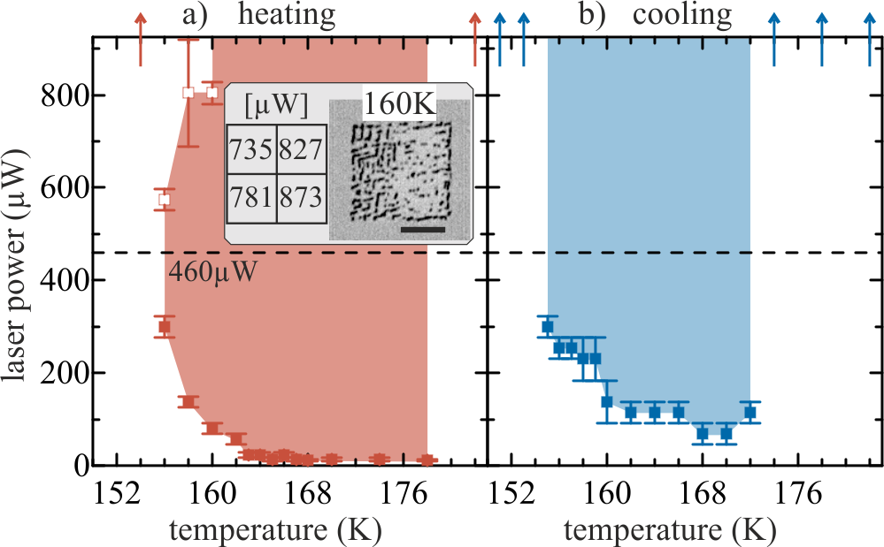
The results are shown in Fig. S3. The temperature range, in which laser irradiation affects the V2O3 film, is larger during heating than during cooling. Further, the minimal power threshold in the heating branch is 11.5 W (at 168 K and 178 K), which corresponds to a theoretical 0.3 mW/m2 peak intensity assuming a Gaussian point spread function. However, the minimal power threshold in the cooling branch is six times larger (69 W, peak intensity 1.7 mW/m2). During heating at low temperatures between 156 K and 160 K, the laser irradiation effect is reduced for high power levels, and the induced phase changes are mainly limited to the edges of the exposed area (see inset Fig. S3(a)). Empty markers in Fig. S3 indicate the corresponding laser power values. A similar effect was not observed during cooling.
IV Thermal effects: minor loop experiment
Since the laser irradiation effect discussed in the main manuscript involves focusing the beam onto a very small region, it is important to check whether the observed phenomenology could simply arise from heating. To address this issue, we performed vs measurements on a continuous 100-nm-thick rf-sputtered V2O3 film on r-cut sapphire [6], with various temperature ramp protocols which would mimic possible laser-induced heating effects. We are aware of the limitation of the difference between smooth adiabatic thermal cycling of the entire thin film and a local laser-induced thermal perturbation.
Here we focus on measurements conducted on the cooling curve where the experiments on laser irradiation described in the main manuscript showed a surprising increase in the insulating phase fraction in considerably large amounts. To check whether a simple heating-cooling thermal cycle may induce a similar effect, we performed the following experiments: first, we warmed the sample up to 210 K to ensure that it is in the fully metallic phase and then slowly cooled it to 154 K which is in the middle of the resistive transition. This reversal temperature exhibits the maximum slope of vs , where the largest effects are expected in resistance change due to the proximity to the percolation threshold. After reaching we performed a minor heating loop, i.e., the sample was heated up by a certain temperature and then cooled down to 100 K. Several runs were conducted with various values of .
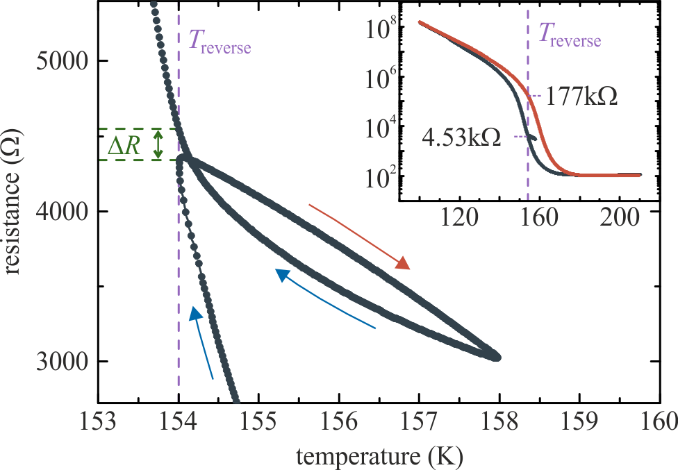
An example of the resistance recorded during such a procedure is shown in Fig. S4 for 4 K which showed the most pronounced effect, i.e., the strongest change in resistance at measured after performing the minor heating loop. During most of this partial temperature cycle the resistance of the minor heating curve is higher than during cooling, as expected. However, as is approached again during cooling the resistance increases and crosses that of the minor heating curve. After completion of the minor thermal cycle, , which corresponds to an increase by % over the starting resistance measured before initiating the minor temperature cycle. This increase in resistance is qualitatively similar to the effect observed in the case of laser irradiation, where after exposure the insulating phase fraction has increased (see panels E-H in Fig. 1(d) in the main manuscript). Contrary to the large effect observed in response to laser irradiation, which drives the film close to thermodynamic equilibrium (increase in filling factor of the insulating phase by % in the middle of the cooling branch; see Fig. 2(c) in the main manuscript), the minor heating cycles result in only a slight increase of % in resistance as compared to the original cooling branch. We note that the minor thermal cycling loop experiments were repeated for several values and that from K to 8 K none showed an increase in resistance at larger than 5 %.
However, quantitatively, it is found that the effect of temperature cycling on the phase fraction is significantly smaller than that of the laser. Considering Fig. 2(c) in the main manuscript, the filling factors of the insulating phase at 157 K after laser exposure and at 155 K before exposure in the cooling branch yield the same value of . Hence, the impact of the laser irradiation in terms of phase filling factors would correspond to a shift in temperature by K. That, in turn, would correspond to a relative change in resistance of % from Fig. 1(a) in the main manuscript. Similar considerations can be made all over the temperature range from 155 K to 168 K in Fig. 2(c) in the main manuscript, and the relative resistance changes are always well above 5 % (see examples in Table 1).
| filling factor of ins. phase | ||||
| (K) | (K) | (K) | (%) | |
| 157 | 155 | 91 | ||
| 160 | 157 | 96 | ||
| 162 | 158 | 83 | ||
| 164 | 160 | 84 | ||
| 166 | 164 | 35 | ||
| 168 | 166 | 22 |
The conclusion that the effect of minor thermal cycles is considerably smaller than that of the laser is further corroborated by the observation that the phase fractions after laser irradiation from both the heating and cooling curves (Fig. 2(c) in the main manuscript) collapse to approximately the same intermediate values between the curves. If the thermal cycling had a similar effect as the laser irradiation, we would expect it to result in a significant rise in resistance close to the mid-point value between the resistances of the cooling curve (4.33 k) and heating curve (177 k) at (see Fig. S4). Since the resistance only increases to 4530 we conclude that the phase fraction after the thermal cycling is much closer to that of the cooling curve than that observed after laser irradiation.
This points to a non-trivial effect of laser irradiation which provides a pathway towards the true equilibrium between the insulating and metallic phases by lowering the free energy barrier between them.
V Mott resistor network simulation
We model and numerically solve our system as a Mott resistor network model as schematized in Fig. S5. A load resistance is making a voltage divider circuit with a resistor tensor network.
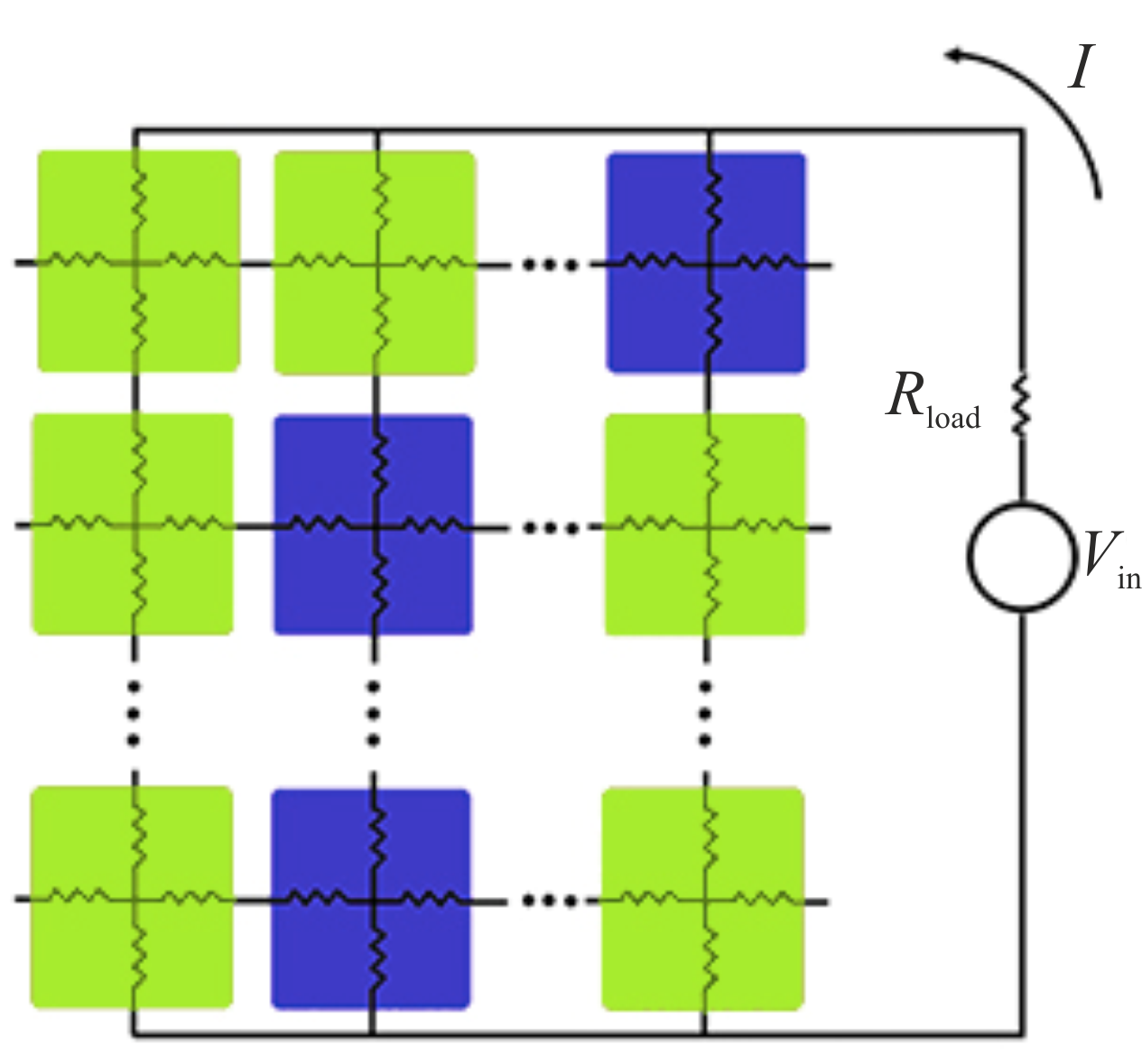
In order to determine the resistance of the entire network, a small bias voltage is applied in order to obtain a voltage across the system
| (S1) |
where denotes the total resistance of the resistor network solved using Kirchhoff laws. Each site of our grid is represented by four resistors of two possible values, and .
In order to simulate the first-order transition we assume a free energy from Landau’s theory with shape [7, 8]
| (S2) |
is the temperature, is an order-parameter-like quantity,
| (S3) |
and
| (S4) |
with a critical temperature , where the free energy is symmetric, and are constant parameters, specified in Table 2.
| (K) | (K) | (K) | (K) | (K) |
| 160 | 87 | -2666.67 | -200 | 4 |
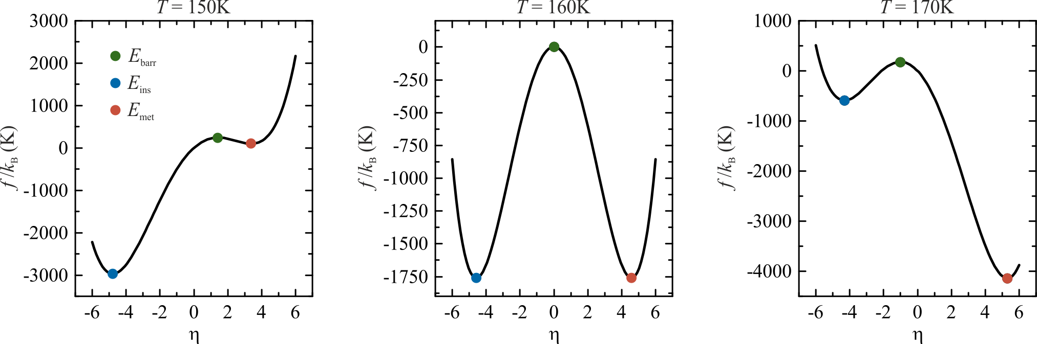
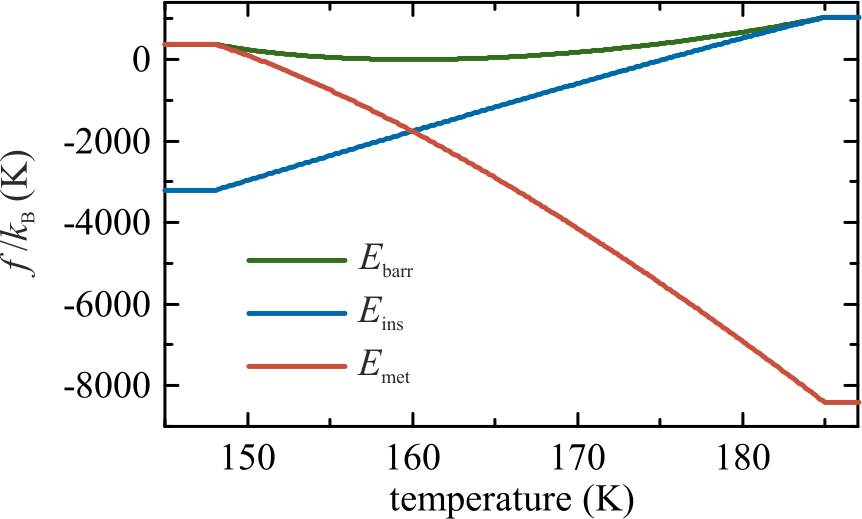
As illustrated for three selected temperatures around in Fig. S6, the free energy exhibits two minima with energies and and one local maximum . The temperature dependence of the energies of these stationary points is shown in Fig. S7.
Each resistor in the network is in a metallic state with energy or in an insulating state with energy . In each simulation cycle, we assign an escape criterion to each site, dependent on whether the initial state is metallic or insulating.
-
•
The criterion to reach the energy barrier from the metallic state is
(S5) -
•
The criterion to reach the barrier from an insulating state is
(S6)
denotes the Boltzmann constant and the energy contribution of the laser in both equations. We generate a random number between zero and one and compare it to the escape criterion of Eq. (S5) or Eq. (S6) with a constant number of iterations, respectively. If the escape criterion exceeds the random number, we assign a resistivity , by assuming Boltzmann weights, with probability
| (S7) |
or with probability
| (S8) |
is the local temperature on the site updated at each cycle by the following formula using the heat equation through the discrete Laplacian approximation
| (S9) |
| (V) | (J/K) | (J/K) | () | () |
| 1 | 0.166 | 10 |
where the indices and denote the coordinates of the site in the network, the substrate temperature, the specific heat of the system, the thermal conductivity and denotes the summation over the first neighbouring sites around the one with coordinates . The constant parameters used in our calculations are summarized in Table 3.
References
- [1]
- [2]
- [3]