Spontaneous localization at a potential saddle point
from edge state reconstruction in a quantum Hall point contact
Abstract
Quantum point contacts (QPCs) are an essential component in mesoscopic devices. Here, we study the transmission of quantum Hall edge modes through a gate-defined QPC in monolayer graphene. We observe resonant tunneling peaks and a nonlinear conductance pattern characteristic of Coulomb-blockaded localized states. The in-plane electric polarizability reveals the states are localized at a classically-unstable electrostatic saddle point. We explain this unexpected finding within a self-consistent Thomas-Fermi model, finding that localization of a zero-dimensional state at the saddle point is favored whenever the applied confinement potential is sufficiently soft compared to the Coulomb energy. Our results provide a direct demonstration of Coulomb-driven reconstruction at the boundary of a quantum Hall system.
Quantum point contacts (QPCs) operated in the quantum Hall regime ubiquitously show resonant tunneling features as edge modes are successively pinched off. These features are generally assumed to arise from uncontrolled disorder potentials introduced, for example, during the fabrication of local split gatesbaer_interplay_2014 ; milliken_indications_1996 ; deprez_tunable_2021 ; zimmermann_tunable_2017 ; ronen_aharonov-bohm_2021 . Here we present evidence that repeatable resonant tunneling features can also arise independently of local disorder via the same Coulomb-interaction driven mechanism that leads to edge-state reconstructionchamon_sharp_1994 . Theoretically, electrostatic confinement in the quantum Hall regime is characterized by the confinement energy, , where is the applied electric potential. The spatial structure of the electron density in the presence of an external potential is controlled by the dimensionless ratio between and the Coulomb energy, . In the sharp-edge regime, , the electron density is expected to decrease sharply and monotonically at the edge of the quantum Hall bulk, leading to the simplest possible (unreconstructed) edge structure. At lower sharpness, corresponding to , a delicate balance between the Coulomb interaction and confining electric potential leads to a more complicated spatial structure in the electron density, which may include a nonmonotonic dependence of the density on position.
Edge-state reconstruction is often invoked as a complicating factor in experiments seeking to probe universal properties of fractional quantum Hall states. For example, the emergence of charge-neutral modes related to edge reconstruction is tied to the suppression of visibility in edge-state interference experimentsbhattacharyya_melting_2019 or the unexpected observation of upstream heat-transport in certain experimentssabo_edge_2017 ; venkatachalam_local_2012 . Universal, reconstruction-free edgeshu_realizing_2011 have been observed using scanning tunneling microscopy at the physical edge of graphene systemsli_evolution_2013 ; coissard_absence_2023 , where the confining potential is atomically sharp. However direct measurements of the edge profile have been elusive at the softer, gate-defined edges that constitute the essential ingredient for mesoscopic devices, such as edge state interferometers, that allow for in situ edge state control.
Here, we study a monolayer graphene device fitted with an electrostatically tunable quantum point contact. Our geometry allows the sharpness of the confinement potential at the QPC to be controlled in situ, allowing us to directly probe the nature of the edge through its effects on the transmission of charge through the point contact. Our main result is an unexpected manifestation of Coulomb-induced reconstruction: the spontaneous formation of a quantum dot localized at an electrostatic saddle point. Our observations imply a local discrepancy between the applied electrostatic potential set by the voltages applied to each gate electrode and the total electronic potential, which takes into account electron-electron interactions and the finite compressibility of the 2DEG at high magnetic fields.
We study a dual-graphite gated hBN-encapsulated graphene van der Waals heterostructure described previously (see cohen_nanoscale_2023 ; cohen_universal_2023 and supplementary information). Local anodic oxidation lithography li_electrode-free_2018 is used to pattern an “X” shape in a graphite flake, which is then integrated into the van der Waals heterostructurecohen_nanoscale_2023 . A subsequent reactive ion etch defines the overall device outline, electrically separating the graphite into four separate gates which we label north (N), south (S), east (E) and west (W). Together, these tune the electron density in each of four quadrants separately. The E and W gates are used to tune the electron density on either side of the device while the N and S gates deplete the electron density to form the QPC constriction. The graphite bottom gate, controlled by a voltage , can be used in conjunction with the top gates to control the fringe-fields at the boundaries between all four regions while maintaining a fixed electron density within the bulk of each quadrant, directly tuning along the edge and at the potential saddle point. This fabrication method, by avoiding subtractive processing in the critical regions of the completed device, results in significantly lower disorder within the quantum point contactcohen_nanoscale_2023 ; cohen_universal_2023 .
To characterize the operation of our QPC we excite an AC voltage on one side of the device and measure the current into a contact on the opposite side of the QPC and the diagonal voltage drop to calculate the four terminal “diagonal conductance”, (see supplementary information). In the integer quantum Hall (IQH) regime this quantity gives a direct measure of the number of edge modes transmitted across the device such that datta_electronic_1995 ; zimmermann_tunable_2017 .
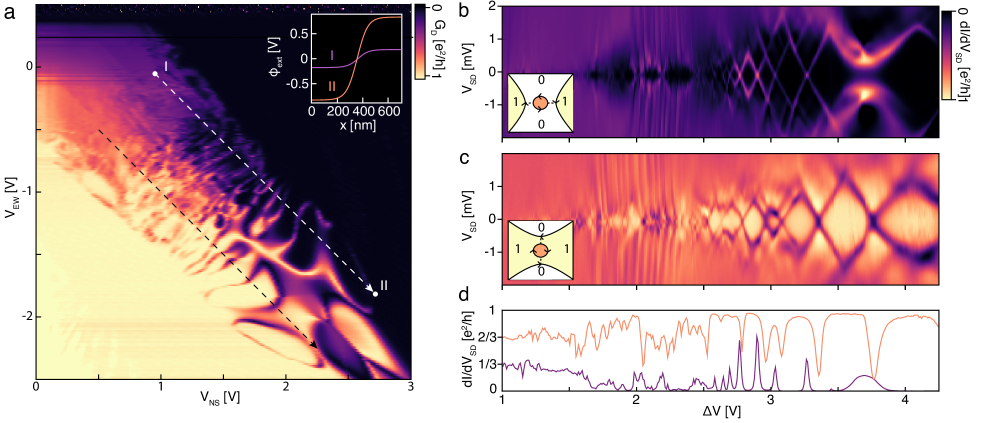
Fig. 1a shows measured over a large range of and at B=13T and with . The plot is centered around the transition between and . The lower left of the plot corresponds to full transmission of the outermost integer quantum Hall edge mode, while lower right corresponds to full pinch-off. The bulk filling factor varies from at to at . Despite the range of bulk filling factors spanned in Fig. 1, varies only from to indicating that only the outermost integer quantum Hall edge mode is transmitted across the device.
Tuning the gate voltages from upper left to lower right in Fig. 1a, corresponding to lines of constant , leaves the applied potential in the middle of the QPC constant. Naively, we expect to also remain constant; however, we observe intricate structure to the measured conductance characterized by the emergence of sharp conductance peaks and dips at the plateau transition. These features are tuned both by the sum and difference of and .
We attribute this structure to the reconstruction of the saddle point potential due to electron-electron interactions. The inset to Fig. 1a shows finite-element simulations of the applied electrostatic potential across the boundary between N and W regions, with the gate voltages set to the values given at the points labelled I and II in Fig. 1a. Within our simulations, can be tuned by more than a factor of four between points I and II, significantly changing the sharpness of the confinement. It is natural to attribute the resonant structure to the effect of this variable; evidently, transmission across the device is highly sensitive to the sharpness of the potential at the the saddle point.
A notable feature of the data in Fig. 1a is the approximate reflection symmetry across the expected line of that relates the two marked trajectories. Figs. 1b and c show the differential conductance across the quantum point contact, , plotted as a function of the source-drain voltage as well as the coordinate parameterizing the contours shown in Fig. 1a. Along the white contour the junction is nearly pinched off, with conductance dropping to zero between high conductance peaks. Nonlinear conductance in this regime shows diamond structure typical of transport across a Coulomb blockaded quantum dot, with charging energies as large as 1 meV. This is consistent with a scenario where resonant transmission through a dot, located at the QPC center, allows charge transport between two otherwise fully-reflected edge states in the E and W regions. This scenario is illustrated schematically in the inset to Fig. 1b.
Along the dashed black arrow in Fig. 1a, nonlinear conductance shows an almost identical diamond structure, except this time with the on-resonance condition corresponding to a decrease in conductance (Fig. 1c). This is again consistent with a Coulomb blockaded quantum dot in the QPC, but one whose effect on transport is to allow backscattering between two otherwise fully-transmitted edge states (see Fig. 1c, inset).
In both scenarios, as is increased, or equivalently, as the potential sharpness is increased, the level spacing of the quantum dot increases. This is consistent with the size of the quantum dot decreasing with increasing , either making the quantum mechanical level spacing smaller, or simply decreasing the island capacitance leading to an increase in the charging energy. Additionally, in Figs. 1b and c, the stability of the Coulomb diamonds decreases with , eventually giving rise to fractional plateaus at and . This is highlighted in Fig. 1d which plots zero-bias data extracted from Figs. 1b and c.
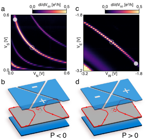
The existence of a quantum dot is not naïvely expected in a quantum point contact where the unscreened electrostatic potential realizes a saddle point. The question thus arises as to whether such behavior can arise intrinsically, or if electron confinement might arise from the presence of uncontrolled impurity potentials near the quantum point contact. To address this question, we use the four-quadrant gate geometry cohen_nanoscale_2023 to determine both the position of the localized charge and its polarizability within the 2D plane. Fig. 2a shows several representative Coulomb blockade peaks as function of and with all other gate voltages constant. The Coulomb peaks follow the condition , where and are the capacitances to the N and S gates, respectively. The ratio of these capacitances may be inferred from the slope of the Coulomb peak trajectory in the plane, . When , we find that , implying that the dot is equidistant from the two gates. The curvature of the peak trajectory, meanwhile, reveals how the capacitances are changed by the motion of the dot. Taking , the curvature is defined by the expression . In Fig. 2a, the curvature is observed to be positive, implying . Since is inversely proportional to the distance between the gate and dot, this implies that a positive bias on repels the dot from the gate, as schematically illustrated in Fig. 2b. This behavior is consistent with a charge trapped at an electrostatic minimum in the N/S direction.
Analogous measurements as a function of and are shown in Fig. 2c. Again, for , , indicating the dot is equidistant from the E and W gates. However, the curvature of the peak trajectories in Fig. 2c are opposite in sign from those in Fig. 2a. This behavior is consistent with a particle trapped in an electrostatic maximum along the E/W direction, as illustrated in Fig. 2d. Taken together, these measurements show that the quantum dot is centered at an electrostatic saddle point. This behavior is consistent across different sets of resonances, different gate voltages, and different magnetic fields, as shown in the Supplementary information. The same characteristic behavior is observed for partial transmission of a quantum Hall edge mode in the absence of resonant behavior, again described in the supplementary. The similarity between the behavior of the quantum dot and the delocalized edge mode supports the idea that the charge in the dot localized precisely at the saddle point. This is a surprising result given that a saddle point potential does not support localized states even in a magnetic field hegde_quasinormal_2019 ; floser_transmission_2010 .
These obsevations can be understood by considering the effects of the Coulomb interaction. Generally, edge state reconstruction may lead to non-monotonic density profiles along a smooth potential step chamon_sharp_1994 ; khanna_fractional_2021 . Along the translation-invariant electrostatic edge between two quantum Hall phases, the resulting electronic density retains the spatial symmetry of the underlying potential, resulting in formation of a series of strips at the boundary between the two phases. In a more complex geometry such as the QPC potential studied here, the same mechanism can favor the formation of more complicated structures that still maintain the 180∘-rotation symmetry of the underlying potential, such as an isolated dot of nonzero density at the center of the QPC.
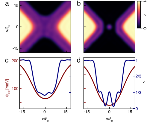
To evaluate the plausibility of a reconstruction-induced quantum dot we use a self-consistent Thomas-Fermi model to calculate the reconstructed density within the QPC. Our calculations account for the density-dependent chemical potential within a partially-filled LL extracted from thermodynamic experimentsyang_experimental_2021 , as well as a realistic device geometry (see supplementary information). Fig. 3a-b shows the calculated density for and . For the softest potential, in panel a, an intermediate side-strip of fractional filling is observed at each boundary between and . As increases, reconstruction becomes less favorable, and an isolated island of filling factor spontaneously forms in the center of the junction. Crucially, this island is isolated from the surrounding regions of non-zero density by depletion regions with . In a transport experiment, these regions may form tunnel barriers between the dot and the reservoirs on either side.
Both regimes of reconstruction correspond directly to observations in Fig. 1. At point I along the dashed white line, where and the applied potential is thus the softest, we observe fractionally-quantized conductance, , corresponding to transmission of a single fractional edge mode, in agreement with Fig. 3a. Additional evidence for the existence of incompressible strips at fractional filling factors within the QPC, maintained over a wide array of electrostatic configurations, is given in supplementary Fig. 5. As is increased to , Coulomb peaks appear corresponding to the existence of a quantum dot as in Fig. 3b. Simulations show that the size of the quantum dot shrinks with further increase of , while the reflected edge mode still maintains strips of away from the QPC, leading to an increase in the level spacing as observed in Fig. 1b-d. At sufficiently large , reconstruction should no longer be favorable anywhere within the device, and one is expected to recover the sharp-edge limit with a single chiral edge mode for a bulk quantum Hall state. As described in the supplementary information, data from a second, identical device shows resonant structure for but a single monotonic step in for . Evidently, for appropriate electrostatic conditions the non-reconstructed limit can be recovered in experiment even for gate defined edges.
Interestingly, within our simulations the quantum dot is composed of an island at fractional filling. This suggests that single fractionally charged quasiparticles can be localized even in a geometry which forbids trapping single particles in the absence of Coulomb interactions. Additionally, in light of our simulations the highly symmetric nature of the resonant reflected features observed in Fig. 1a may likely be interpreted as the particle-hole conjugate to the scenario presented in Fig. 3b. Future experiments, for example measuring the shot noise across the QPC, may give direct evidence for the trapping of fractional quasiparticles in the saddle-point quanutm dot.
In conclusion, we have shown that QPCs in the quantum Hall regime can host Coulomb blockade physics even in the absence of an applied confining potential or disorder effects, resulting from the spontaneous formation of a quantum dot due to the interplay between the applied gate potential and interparticle Coulomb interactions. The discrepancy between the applied electrostatic potential and the total potential at the QPC provides direct evidence for edge state reconstruction. By characterizing edge-state reconstruction in comparatively simple direct current transport measurements, moreover, we show that these effects may be identified and mitigated in experiments to probe fractional statistics in graphene based devices using QPCszimmermann_tunable_2017 ; cohen_nanoscale_2023 ; cohen_universal_2023 and Fabry-Perot interferometersronen_aharonov-bohm_2021 ; deprez_tunable_2021 ; fu_aharonov-bohm_2023 ; werkmeister_strongly_2023 ; zhao_graphene-based_2022 .
Acknowledgements.
The authors thank J. Folk and A. Potts for comments on the manuscript. Work at UCSB was primarily supported by the Air Force Office of Scientific Research under award FA9550-20-1-0208 and by the Gordon and Betty Moore Foundation EPIQS program under award GBMF9471. LC and NS received additional support from the Army Research Office under award W911NF20-1-0082. TW and MZ were supported by the Director, Office of Science, Office of Basic Energy Sciences, Materials Sciences and Engineering Division of the U.S. Department of Energy under contract no. DE-AC02-05-CH11231 (van der Waals heterostructures program, KCWF16). KK was supported by the U.S. Department of Energy, Office of Science, National Quantum Information Science Research Centers, Quantum Science Center. CR was supported by the National Science Foundation through Enabling Quantum Leap: Convergent Accelerated Discovery Foundries for Quantum Materials Science, Engineering and Information (Q-AMASE-i) award number DMR-1906325. K.W. and T.T. acknowledge support from JSPS KAKENHI (Grant Numbers 19H05790, 20H00354 and 21H05233).I References
References
- (1) Baer, S. et al. Interplay of fractional quantum Hall states and localization in quantum point contacts. Physical Review B 89, 085424 (2014).
- (2) Milliken, F. P., Umbach, C. P. & Webb, R. A. Indications of a Luttinger liquid in the fractional quantum Hall regime. Solid State Communications 97, 309–313 (1996).
- (3) Déprez, C. et al. A tunable Fabry-Pérot quantum Hall interferometer in graphene. Nature Nanotechnology 16, 555–562 (2021).
- (4) Zimmermann, K. et al. Tunable transmission of quantum Hall edge channels with full degeneracy lifting in split-gated graphene devices. Nature Communications 8, 14983 (2017).
- (5) Ronen, Y. et al. Aharonov-Bohm effect in graphene-based Fabry-Pérot quantum Hall interferometers. Nature Nanotechnology 16, 563–569 (2021).
- (6) Chamon, C. d. C. & Wen, X. G. Sharp and smooth boundaries of quantum Hall liquids. Physical Review B 49, 8227–8241 (1994).
- (7) Bhattacharyya, R., Banerjee, M., Heiblum, M., Mahalu, D. & Umansky, V. Melting of Interference in the Fractional Quantum Hall Effect: Appearance of Neutral Modes. Physical Review Letters 122, 246801 (2019).
- (8) Sabo, R. et al. Edge reconstruction in fractional quantum Hall states. Nature Physics 13, 491–496 (2017).
- (9) Venkatachalam, V., Hart, S., Pfeiffer, L., West, K. & Yacoby, A. Local thermometry of neutral modes on the quantum Hall edge. Nature Physics 8, 676–681 (2012).
- (10) Hu, Z.-X., Bhatt, R. N., Wan, X. & Yang, K. Realizing Universal Edge Properties in Graphene Fractional Quantum Hall Liquids. Physical Review Letters 107, 236806 (2011).
- (11) Li, G., Luican-Mayer, A., Abanin, D., Levitov, L. & Andrei, E. Y. Evolution of Landau levels into edge states in graphene. Nature Communications 4 (2013).
- (12) Coissard, A. et al. Absence of edge reconstruction for quantum Hall edge channels in graphene devices. Science Advances 9, eadf7220 (2023).
- (13) Cohen, L. A. et al. Nanoscale electrostatic control in ultraclean van der Waals heterostructures by local anodic oxidation of graphite gates. Nature Physics 19, 1502–1508 (2023).
- (14) Cohen, L. A. et al. Universal chiral Luttinger liquid behavior in a graphene fractional quantum Hall point contact. Science 382, 542–547 (2023).
- (15) Li, H. et al. Electrode-Free Anodic Oxidation Nanolithography of Low-Dimensional Materials. Nano Letters 18, 8011–8015 (2018).
- (16) Datta, S. Electronic Transport in Mesoscopic Systems. Cambridge Studies in Semiconductor Physics and Microelectronic Engineering (Cambridge University Press, Cambridge, 1995).
- (17) Hegde, S. S., Subramanyan, V., Bradlyn, B. & Vishveshwara, S. Quasinormal Modes and the Hawking-Unruh Effect in Quantum Hall Systems: Lessons from Black Hole Phenomena. Physical Review Letters 123, 156802 (2019).
- (18) Flöser, M., Champel, T. & Florens, S. Transmission coefficient through a saddle-point electrostatic potential for graphene in the quantum Hall regime. Physical Review B 82, 161408 (2010).
- (19) Khanna, U., Goldstein, M. & Gefen, Y. Fractional edge reconstruction in integer quantum Hall phases. Physical Review B 103, L121302 (2021).
- (20) Yang, F. et al. Experimental Determination of the Energy per Particle in Partially Filled Landau Levels. Physical Review Letters 126, 156802 (2021).
- (21) Fu, H. et al. Aharonov-Bohm oscillations in bilayer graphene edge state Fabry-P\’erot interferometers. Nano Letters 23, 718–725 (2023).
- (22) Werkmeister, T. et al. Strongly coupled edge states in a graphene quantum Hall interferometer (2023). ArXiv:2312.03150 [cond-mat].
- (23) Zhao, L. et al. Graphene-Based Quantum Hall Interferometer with Self-Aligned Side Gates. Nano Letters 22, 9645–9651 (2022).