Terahertz emission from -W/CoFe epitaxial spintronic emitters
Abstract
We report efficient terahertz (THz) generation in epitaxial -W/Co60Fe40 spintronic emitters. Two types of emitters have been investigated; epitaxial -W/Co60Fe and -W/Co60Fe deposited on single crystalline Al2O3() and MgO() substrates, respectively. The generated THz radiation is about larger for -W/Co60Fe grown on single crystalline Al2O3(), which is explained by the fact that the -W/Co60Fe interface for this emitter is more transparent to the spin current due to the presence of Ångström-scale interface intermixing at the W/CoFe interface. Our results also reveal that the generation of THz radiation is larger when pumping with the laser light from the substrate side, which is explained by a larger part of the laser light due to interference effects in the film stack being absorbed in the ferromagnetic Co60Fe40 layer in this measurement configuration.
I Introduction
Terahertz (THz) radiation is typically defined from 0.3 to 30 THz of the electromagnetic spectrum corresponding to a wavelength range of 1 mm to 10 m. The terahertz frequency range lies between the microwave and near infrared regions of the electromagnetic spectrum and has traditionally been called the terahertz gap due to the difficulties in generating THz radiation. This has limited its use despite of a large number of possible applications [1, 2, 3]. Techniques used for generation of THz radiation include photoconductive switching, optical rectification, transient photo-current in air plasma and difference frequency generation [4, 5, 6, 7, 8, 9, 10, 11, 12, 13]. A more recent technique builds on the spin degree of freedom in magnetic heterostructures [14, 15, 16]. This technique has the advantage of generating broadband radiation and with intensity levels comparable to the standard zinc telluride source.
A magnetic heterostructure generating THz radiation, referred to as a spintronic THz emitter (STE), typically consists of a heavy metal (HM) with strong spin-orbit interaction and a ferromagnetic (FM) material. It is well established that a femto-second laser pulse leads to a demagnetization process of the FM layer and the generation of an ultrafast superdiffusive spin current () [17]. The transfer of spin current across the FM/HM interface will via the inverse spin Hall effect (ISHE) [18] or the the inverse Rashba-Edelstein effect (IREE) [19] generate a transient charge current () in the HM layer that emits THz radiation. Critical parameters for the emission of THz radiation are the spin-to-charge conversion efficiency characterized by the spin Hall angle () of the HM, , and the transparency of the FM/HM interface characterized by the effective spin-mixing conductance () of the interface [20, 21]. The effective spin-mixing conductance describes the transfer of spin current across the interface and accounts for spin-backflow as well as spin-memory loss at the interface, emphasizing the importance of the interface quality for STEs. For example, large interface roughness may lead to spin memory loss at the interface [22].
Tungsten may crystallize in the ground-state -W phase or in the metastable -W phase. Interestingly, the high-resistivity -W phase (cm) has been reported to exhibit a giant SHE with a spin Hall angle to [23, 24, 25], while the low-resistivity -W phase (cm) exhibits a more modest value of the spin Hall angle (). electronic structure calculations have revealed that the spin Hall conductivity () for the -W phase is about larger than that of the -W phase [24]. It is clear that this difference in spin Hall conductivity alone cannot explain the difference in spin Hall angle. However, considering that the spin Hall angle can be expressed as , it becomes clear that the difference is a combined effect of the spin Hall conductivity and the much larger resistivity of the -W phase.
It has been argued from first-principle calculations that the Dirac fermions appearing in the -W phase are important to understand its giant spin Hall effect [26], since according to a separate study, Dirac fermions have been identified to generate Berry-curvature-induced spin Hall conductivity [27]. Interestingly, the presence of topological surface states in tungsten was first predicted by Thonig . [28] for the -W phase. Moreover, it has been reported that these surface states predominately appear in certain crystallographic planes [26, 28, 29, 30].
In this study, we have investigated the THz emission from epitaxial -W/Co60Fe40 spintronic emitters. Two types of emitters have been investigated, deposited on single crystalline Al2O3 () and MgO () substrates. A strong motivation for choosing these substrates is that they provide two different interfaces for tungsten; namely -W in case of Al2O3 () [31] and -W in case of MgO [32]. It has been shown that the -W(110) interface exhibits Dirac-type surface states [28] and more recently it has also been shown that the -W(100) interface exhibits Dirac-type surface states [30], which is believed to have a direct impact on the spin Hall angle and therefore also on the spin-to-charge conversion of the STE. It is therefore motivated to investigate if the two interfaces are different in this respect and if there are other interface related properties that may affect the emision of THz radiation.
II Methods
II.1 Growth
Magnetic heterostructures consisting of -W/Co60Fe40 (henceforth referred to as W/CoFe) bilayers with different layer thicknesses ranging from to nm were deposited on single crystalline Al2O3 () and MgO () substrates (both 1010 mm2) at floating potential, using direct current (dc) magnetron sputtering. Except for the W()/CoFe(3) series of samples (numbers within parentheses refer to layer thickness in nm), which were deposited on double-sided polished Al2O3 (), the films were deposited on single-sided polished substrates. Prior to deposition, the substrates were cleaned in acetone and 2-propanol using ultrasonic agitation for 120 s each. This was followed by annealing in vacuum at 873(2) K for 1 hour. The base pressure of the growth chamber was below 510-7 Pa. In order to prevent surface oxidation of the films, the samples were capped at ambient temperature ( 313(2) K) with Al2O3 using radio frequency (rf) magnetron sputtering. The depositions were carried out in an Ar atmosphere at pressure of 310-2 Pa (gas purity 99.999 %) from an elemental W (25 W, dc) target, and CoFe (13 W, dc) and Al2O3 (90 W, rf) compound targets. The targets were cleaned by sputtering against closed shutters for at least 60 s prior to each deposition. The target-to-substrate distance in the deposition chamber was around 0.2 m. The deposition rates (W: 0.253 Å/s, Al: 0.30 Å/s, CoFe: 0.10 Å/s, Al2O3: 0.03 Å/s) were calibrated prior to the growth using X-ray reflectivity. The W growth temperature was optimized with respect to W layering and crystal quality, yielding 843(2) K for single W layers. For the W/CoFe bilayers, W and CoFe were grown at 843(2) K and 573(2) K, respectively. Finally, in order to ensure thickness uniformity, the substrate holder was rotated during the deposition.
II.2 Characterization
A THz time-domain spectrometer was employed to measure the THz emission from the W/CoFe heterostructures [15, 33]. This spectrometer utilized a Spectra-Physics Tsunami laser source, which generated pulses with a duration of fs (bandwidth nm, central wavelength nm, and maximum output energy nJ) at a repetition rate of 80 MHz. A low-temperature gallium arsenide photoconductive dipole antenna with m gap was used as a detector for the THz pulses. A probe beam with an average laser power of 10 mW was used for the detection and a static in-plane magnetic field of mT was used to saturate the magnetization of the W/CoFe films. Recorded THz signals correspond to averages of 500 detected THz spectra obtained within one minute of the measurement time.
Transmission electron microscopy (TEM) and scanning TEM (STEM) were performed in a double aberration-corrected Themis Z (Thermo Fisher), which was operated at 300 kV and equipped with a low-background double-tilt holder and a Super-X EDS detector. The aberrations were corrected up to 5th order. STEM imaging and EDS acquisition and analyses were acquired using a Thermo Fisher Velox. The convergent angle of the probe and collection angle for high-angle annular dark-field (HAADF) imaging were 16 and 63-200 mrad, respectively. TEM and selected-area electron diffraction were recorded using a Gatan OneView camera.
X-ray reflectometry (XRR) and diffraction (XRD) were carried out in a Bede D1 diffractometer equipped with a Cu x-ray source operated at 35 mA and 50 kV. A circular mask (diameter: 0.005 m) and an incidence and a detector slit (both 0.0005 m) were used. For monochromatizing the beam by reducing the CuK and CuK radiation, the setup included a Göbel mirror and a 2-bounce-crystal on the incidence side. The x-rays were detected with a Bede EDRc x-ray detector. The XRR results for the STEs studied here are presented in Supplementary Information (SI), Tables ST1-ST4. The XRD results, described elsewhere [34], show that -W grows epitaxially in the [] growth direction on Al2O3 () and in the [] growth direction on MgO (). The crystalline quality for -W grown on Al2O3 is better, as indicated by a much smaller mosaic spread of the crystal plane orientations. It should be noted though that -W grown on MgO exhibits a highly preferential [001] growth orientation.
A Quantum Design magnetic property measurement system was used to assess the magnetic properties of samples; results from room temperature magnetization versus in-plane magnetic field measurements are presented in SI, Fig. S1. The saturation magnetization values for CoFe in the thickness range nm are slightly smaller than values reported for thicker films [35]. An AIT CMT-SR2000N 4-point probe measurement system was used to measure the sheet resistance of -W films with thicknesses in the range nm. The low resistivity of the measured samples (cf. Fig. S2 in SI) confirms the -phase for the epitaxial W layers.
In an attempt to determine the optical absorptance of the investigated film stacks, reflectance () and transmittance () spectra were measured using an integrated sphere, Perkin Elmer Lambda 900 double beam spectrophotometer equipped with a cm spectralon-coated sphere. The scattered and regular/specular light signals entering the sphere have to be corrected in different ways for sphere wall reflectance and hence, both total and scattered spectra were recorded in both reflectance and transmittance modes [36, 37, 38]. The absorptance was then calculated as . The calculated absorptance is the total absorptance of the film stack. Schematic illustrations of the sphere geometry in reflectance and transmittance modes are shown in SI, Fig. S3.
Standard Fresnel calculations were performed for film stacks with different compositions and thickness [39, 40]. The film stack configuration is illustrated in SI, Fig. S4. Such calculations are to some extent uncertain because the included films are very thin, and the optical constants are slightly uncertain. It is well known that the optical constants of very thin films may differ from the optical constants of thick films or bulk materials. Calculations are useful, however, as it is simple and straight forward to vary the composition of the film stack and to get an indication of how film thickness influences the optical properties of the samples. The optical constants for the different layers and substrates used were taken from the literature [41, 42]. The optical constants for the CoFe film was taken as the average value of the constants for Co and Fe. Possible absorption in the oxide substrates was not considered in the calculations.
III Results and discussion
HAADF-STEM images and EDS maps of W/CoFe layers on Al2O3 and MgO substrate are shown in Fig. 1.
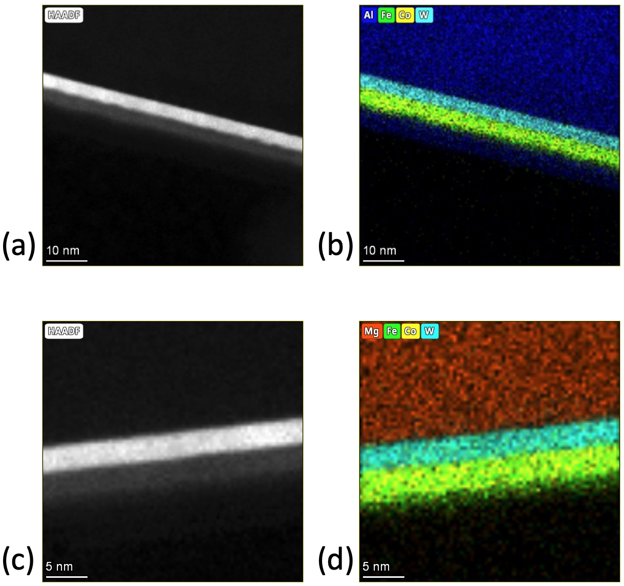
The contrast of HAADF images, known as Z-contrast, clearly distinguishes the layers, including the Al2O3 capping layer. The estimated thicknesses of the W and CoFe layers are nm and nm on the Al2O3 substrate and nm and nm on the MgO substrate, respectively. The EDS maps confirm that the element distributions are confined in each layer. High-resolution HAADF-STEM images, shown in Fig. 2 (c) and (d), illustrate the epitaxial relationship between substrate and layers by the alignment of lattice planes. In the case of the MgO substrate, the interface between the W and CoFe layers is atomically flat, while intermixing about a few atomic layers, is observed for the Al2O3 substrate. Moreover, the high-resolution HAAD-STEM images indicate that interface intermixing has occurred at the W/CoFe interface for this substrate. In addition to HAADF-STEM imaging, HRTEM images were taken in order to obtain other information than atomic species and thickness. Figure 2 (a) and (b) show the HRTEM images of W/CoFe on Al2O3 and MgO substrate, respectively. The alignment of lattice planes in W, CoFe and the substrates are consistent with the HAADF results.
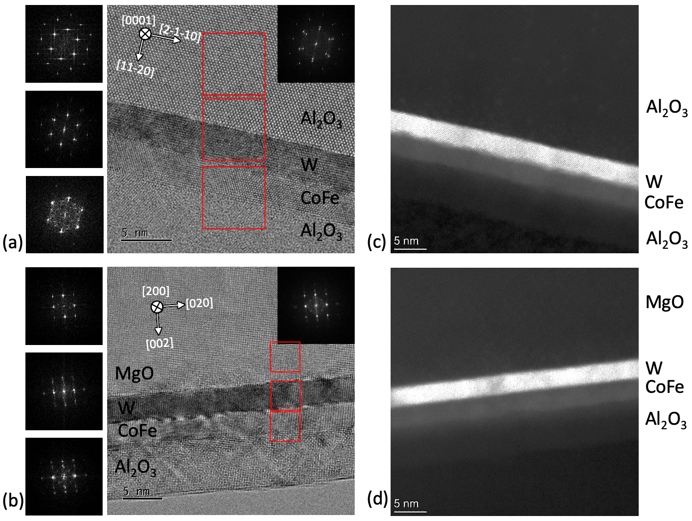
The insets are the fast Fourier transform (FFT) of the HRTEM images, which are similar to selected area electron diffraction patterns shown in SI, Figs. S5 and S6. In addition, the FFTs of the selected regions, highlighted in red squares, show the orientations. All FFTs confirm the epitaxial relationship. In the case of the Al2O3 substrate (Fig. 2 (a)), the interface between the W and CoFe layers looks smoother than indicated by HAADF-STEM. It is worth noting that the imaging mechanisms of HRTEM are phase and diffraction contrast that are sensitive to crystallographic orientation and defects but not to the atomic number as in HAADF. The asymmetric contrasts of different lattice fringes indicate a slight but detectable crystallographic misorientation from the zone axis. By contrast, the interface in the film deposited on MgO exhibits more localized bright/dark contrasts. These additional contrasts indicate the presence of local strain, where distortion of lattice fringes and edge dislocations are expected.
Figure 3(a) shows the generated THz electric field in time domain for two W/CoFe spintronic emitters deposited on Al2O3 () and MgO () substrates when pumping from the substrate side. Note that the polarity of the THz waveform is reversed when reversing the magnetization direction while keeping the pumping side the same (cf. Fig. S7 in SI). Thus, the THz emission is clearly of magnetic origin. Figure 3(b) shows the THz electric field peak-to-peak amplitude versus laser power for the same STEs. As expected, the peak-to-peak amplitude increases linearly at low laser power, but the increase slows down above mW laser power and the amplitude reaches a maximum at about mW laser power followed by a weak decrease of the amplitude on further increase of the laser power. Similar behaviour has previously been observed and can be attributed to a spin accumulation effect and the laser-induced heating effect [43, 44, 45]. The spin accumulation effect implies that there is an upper limit for the density of spin-polarized electrons in the HM, while the heating effect induces a large enough increase of the spin temperature to weaken the magnetization of the ferromagnetic layer [46]. The figure also indicates that the emitted THz electric field is about larger for the STE grown on the Al2O3 () substrate. It is tempting to attribute this difference to the Dirac-type surface states shown to exist in -W(110) [28]. However, first-principle calculations show that Dirac-type surface states also exist in -W(001) [30]. Another possible explanation for the difference in THz electric field amplitude is connected to the transparency of the -W/CoFe interface characterized by the effective spin-mixing conductance. The influence of interface intermixing on the spin-mixing conductance has been quantitatively studied for Pt/Py (Py = Permalloy) bilayers using first-principles calculations [47]. The interface intermixing was modelled as a scattering region consisting of composite Pt1-xPyx and PtxPy1-x layers for the first Pt and Py atomic layers at the interface. Comparing with the spin-mixing conductance for an ideally clean and atomically flat interface, corresponding to , it was found that the spin-mixing conductance is enhanced in the presence of interface intermixing. Moreover, experimental support for this has been obtained for Co/Pt bilayers [48]. An ultrahin layer of the composite CoxPt1-x was in this work introduced between the Co and Pt layers to study the effect of interface intermixing, clearly revealing that interface intermixing enhances THz emission. Based on the information obtained from the high-resolution HAADF-STEM images, we conclude that the enhanced THz electric field amplitude for the STE grown on the Al2O3 () substrate is a result of an Ångström-scale scattering region at the interface consisting of a few atomic composite layers as described in the first-principles calculations [47]. Considering the high crystalline quality of the bilayers studied here, we are not considering the effect of strongly disordered interfaces on the spin-mixing conductance and THz emission.
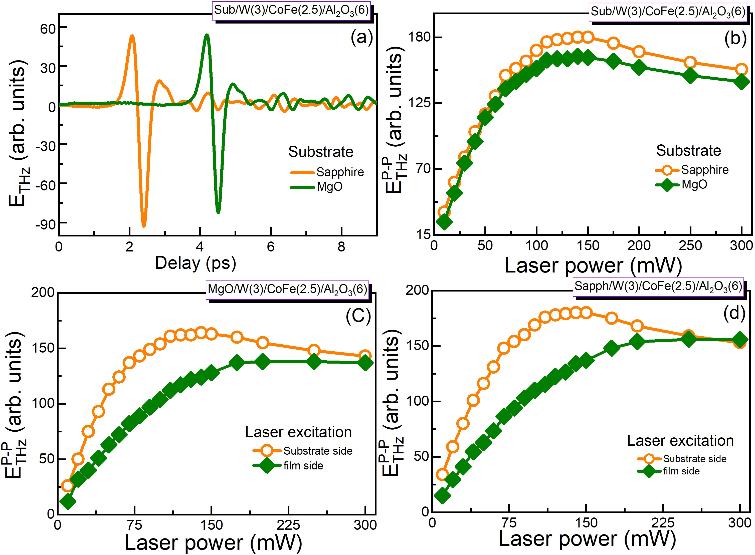
Figures 3 (c) and (d) show, respectively the THz electric field peak-to-peak amplitude for MgO/W()/CoFe()/Al2O3() and sapphire/W()/CoFe()/Al2O3() versus laser power when pumping from the substrate and film sides. For both STEs, the generated THz electric field is significantly larger when pumping from the substrate side. The only plausible explanation for this is that more laser power is absorbed when pumping from the substrate side and that therefore a larger spin current is generated. This will be further discussed below.
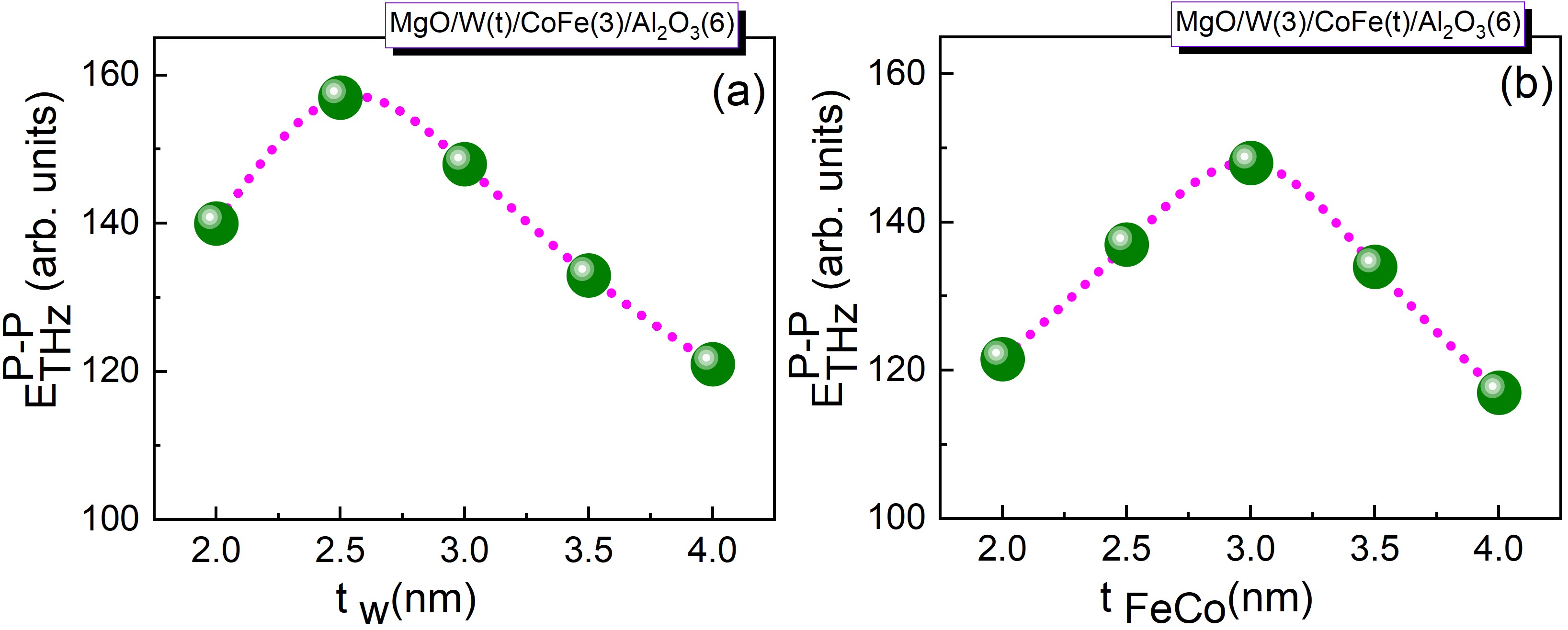
Figure 4 shows the variation of the THz electric field peak-to-peak amplitude with thickness of the W and CoFe layers. The largest amplitude is obtained for a W thickness of nm and a CoFe thickness of nm.
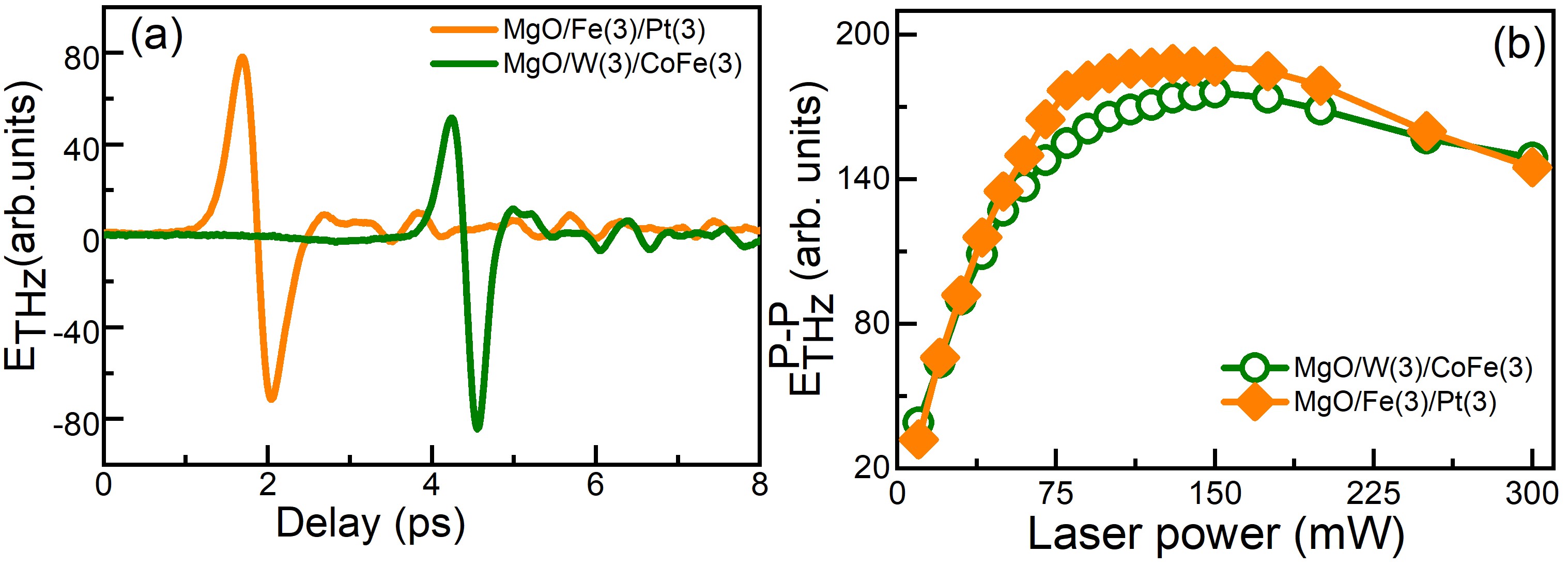
It is interesting to compare the -W/Co60Fe40 STE investigated here with a standard bilayer STE like Fe/Pt [45]. We therefore deposited a MgO/Fe(3)/Pt(3) STE for comparison with our -W based STEs. Figures 5 (a) and (b) show the THz electric field waveform in time domain and the peak-to-peak amplitude versus laser power for MgO/W()/CoFe() and MgO/Fe()/Pt(), respectively. The emitted THz signals are comparable for these two STEs, even though it should be noted that the MgO/Fe/Pt STE exhibits larger THz amplitude decreasing the thickness of the Pt layer (cf. Fig. S8 in SI).
There is a considerable difference in optical properties between the two measurement orientations, as light beams reflected from the two surfaces of the substrate are non-coherent and are not subject to interference effects. The aluminium-oxide cap on the film side, on the other hand, is very thin and thus interference occurs between multiply reflected beams. The surface texture of the back surface of the substrate also causes light to be scattered in different ways in the front and back configurations. These two effects result in the fact that the transmittance and reflectance spectra are different for the two measurement orientations. The difference in absorptance caused by interference is illustrated in Fig. 6(a), where the reflectance, transmittance and absorptance spectra for the W(3)/CoFe(3) emitter are shown. This sample was prepared on a double-sided polished Al2O3 () substrate, implying that there is no surface texture on the back surface of the substrate. It can be seen that for this sample the reflectance is quite different between the light being incident from the substrate and film sides while the transmittance is the same. In both orientations the diffuse signals are close to zero. This means that the absorptance is higher for light incident from the substrate side, which in turn implies that one can expect a stronger spin current to be generated for this orientation.
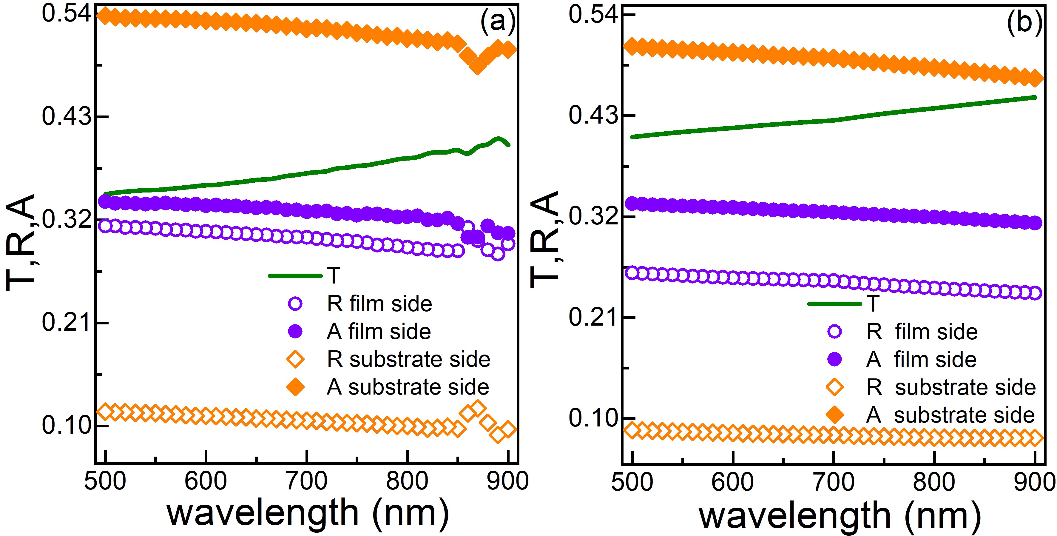
For the other STEs the surface texture on the back surface of the substrate causes diffuse (scattered) signals , which complicates the situation. The transmittance is in these cases not the same from the two sides and both reflectance and transmittance differ. This can be seen in Fig. S9 in SI. However, accounting for the diffuse scattering it can be seen that the absorptance for all STEs is higher for light incident from the substrate side.
A problem with the results from calculations is that these do not take light scattering into account, but the results indicate that the trends with varied input parameters are consistent with our experimental results. The sample with a smooth back surface can be used to compare experimental and calculated results with no scattering involved. This is shown in Fig. 6(b). It can be seen that the trends with the difference in reflectance and absorptance when light is incident on the film and substrate sides of the sample are consistent. Considering the extremely thin layers these Fresnel calculations are very encouraging.
The property of interest in this investigation is thus the absorptance within the film stack. Neither the experimental results, nor the calculated results, provide information about exactly where in the film stack absorption occurs. It is obvious, however, that the absorption mechanism is within the two metallic layers. Owing to the similarity of the optical constants of W, Co and Fe, the absorption is likely to be similar in the two metallic layers (W and CoFe). Both the calculated results and the experimental results indicate that the absorptance is higher when light is incident from the substrate side. The absorptance also increases with film thickness of the CoFe layer, which is also as expected. These results are shown in Fig. S10 in SI for measured and calculated absorptance. The trend is the same for all results, but there is a difference as the experimental results take light scattering into account while the calculated spectra assume ideally flat interfaces.
An unexpected result was revealed when comparing the THz emission between STEs grown on double-sided and single-sided polished substrates. THz electric field in time domain for sapphire/W()/CoFe()/Al2O3() and MgO/W()/CoFe()/Al2O3() when pumping from substrate and film sides are shown in Fig. S11 in SI. The former STE was grown on double-sided polished substrate, while the latter was grown on single-sided polished substrate. The THz electric field is about () larger for the STE grown on the Al2O3 () double (single) sided polished substrate compared to MgO single-sided polished substrate. The THz electric field amplitude is significantly larger for the film grown on the double-sided polished substrate when pumping from the substrate side. A possible explanation for this result is that the substrates used in this study have some absorption. When pumping from the substrate side, considering light scattering at the substrate back surface, the light will travel a longer path inside the substrate thereby yielding increased absorption in the substrate. Increased absorption in the substrate in turn implies less light reaching the magnetic layer and therefore a reduced spin current and emission of THz radiation.
IV Conclusion
To summarize, we provide direct evidence of THz emission in epitaxial -W/Co60Fe40 spintronic emitters. Two types of emitters have been investigated; epitaxial -W/Co60Fe and -W/Co60Fe deposited on single crystalline Al2O3() and MgO() substrates, respectively. The generated THz radiation is about larger for the -W/Co60Fe emitter, which might be linked to a difference in topological surface states appearing in -W and -W. However, a more plausible explanation is that the -W/Co60Fe interface is more transparent to the spin current due to the presence of Ångström-scale interface intermixing at the W/CoFe interface. Results from first-principles calculations show that the spin-mixing conductance is enhanced in the presence of interface intermixing [47]. Our results also reveal that the generation of THz radiation is larger when pumping with the laser light from the substrate side. Measurements of reflectance and transmittance spectra as well as Fresnel calculations for the studied film stacks show that this can be explained by a larger part of the laser light being absorbed in the ferromagnetic Co60Fe40 layer in this measurement configuration due to interference effects. A comparison with the reference Fe/Pt STE, which is known to provide one of the highest THz signals [16], shows that the emitted W/CoFe THz electric field amplitude is of similar magnitude. It is also worth noting that light scattering at the substrate back surface may suppress the amplitude of the emitted THz electric field amplitude by increased absorption of the laser light in the substrate.
V acknowledgments
This work is supported by the Swedish Research Council (grant numbers 2021-04658 and 2019-03581) and Olle Engkvists Stiftelse (grant number 182–0365). This work was performed, in part, at the Electron Microscopy Centre, supported by the Department of Materials and Environmental Chemistry and Faculty of Science at Stockholm University, Sweden.
References
- Valušis et al. [2021] G. Valušis, A. Lisauskas, H. Yuan, W. Knap, and H. G. Roskos, Sensors 21 (2021).
- Federici and Moeller [2010] J. Federici and L. Moeller, J. Appl. Phys. 107, 6 (2010).
- Leitenstorfer et al. [2023] A. Leitenstorfer, A. S. Moskalenko, T. Kampfrath, J. Kono, E. Castro-Camus, K. Peng, N. Qureshi, D. Turchinovich, K. Tanaka, A. G. Markelz, M. Havenith, C. Hough, H. J. Joyce, W. J. Padilla, B. Zhou, K.-Y. Kim, X.-C. Zhang, P. U. Jepsen, S. Dhillon, M. Vitiello, E. Linfield, A. G. Davies, M. C. Hoffmann, R. Lewis, M. Tonouchi, P. Klarskov, T. S. Seifert, Y. A. Gerasimenko, D. Mihailovic, R. Huber, J. L. Boland, O. Mitrofanov, P. Dean, B. N. Ellison, P. G. Huggard, S. P. Rea, C. Walker, D. T. Leisawitz, J. R. Gao, C. Li, Q. Chen, G. Valušis, V. P. Wallace, E. Pickwell-MacPherson, X. Shang, J. Hesler, N. Ridler, C. C. Renaud, I. Kallfass, T. Nagatsuma, J. A. Zeitler, D. Arnone, M. B. Johnston, and J. Cunningham, Journal of Physics D: Applied Physics 56, 223001 (2023).
- Smith et al. [1988] P. R. Smith, D. H. Auston, and M. C. Nuss, IEEE Journal of Quantum Electronics 24, 255 (1988).
- Venkatesh et al. [2014] M. Venkatesh, K. Rao, T. Abhilash, S. Tewari, and A. Chaudhary, Optical Materials 36, 596 (2014).
- Lepeshov et al. [2017] S. Lepeshov, A. Gorodetsky, A. Krasnok, E. Rafailov, and P. Belov, Laser & Photonics Reviews 11, 1600199 (2017).
- Yang et al. [2007] Z. Yang, L. Mutter, M. Stillhart, B. Ruiz, S. Aravazhi, M. Jazbinsek, A. Schneider, V. Gramlich, and P. Günter, Advanced Functional Materials 17, 2018 (2007).
- Kim et al. [2021] S.-J. Kim, B. J. Kang, U. Puc, W. T. Kim, M. Jazbinsek, F. Rotermund, and O.-P. Kwon, Advanced Optical Materials 9, 2101019 (2021).
- Vediyappan et al. [2019] S. Vediyappan, A. K. Chaudhary, V. Mottamchetty, R. Arumugam, V. Gandhiraj, M. Senthil Pandian, and R. Perumalsamy, Crystal Growth & Design 19, 6873 (2019).
- Kim et al. [2007] K.-Y. Kim, J. H. Glownia, A. J. Taylor, and G. Rodriguez, Optics express 15, 4577 (2007).
- Yan et al. [2017] D. Yan, Y. Wang, D. Xu, P. Liu, C. Yan, J. Shi, H. Liu, Y. He, L. Tang, J. Feng, et al., Photonics Research 5, 82 (2017).
- Lu et al. [2017] C. Lu, C. Zhang, L. Zhang, X. Wang, and S. Zhang, Physical Review A 96, 053402 (2017).
- Fülöp et al. [2020] J. A. Fülöp, S. Tzortzakis, and T. Kampfrath, Advanced Optical Materials 8, 1900681 (2020).
- Seifert et al. [2016] T. Seifert, S. Jaiswal, U. Martens, J. Hannegan, L. Braun, P. Maldonado, F. Freimuth, A. Kronenberg, J. Henrizi, I. Radu, et al., Nat. Photonics 10, 483 (2016).
- Gupta et al. [2021a] R. Gupta, S. Husain, A. Kumar, R. Brucas, A. Rydberg, and P. Svedlindh, Adv. Opt. Mater. 9, 2001987 (2021a).
- Papaioannou and Beigang [2021] E. T. Papaioannou and R. Beigang, Nanophotonics 10, 1243 (2021).
- Battiato et al. [2010] M. Battiato, K. Carva, and P. M. Oppeneer, Phys. Rev. Lett. 105, 027203 (2010).
- Sinova et al. [2015] J. Sinova, S. O. Valenzuela, J. Wunderlich, C. H. Back, and T. Jungwirth, Rev. Mod. Phys. 87, 1213 (2015).
- Sánchez et al. [2013] J. C. R. Sánchez, L. Vila, G. Desfonds, S. Gambarelli, J. P. Attané, J. M. De Teresa, C. Magén, and A. Fert, Nature Communications 4, 2944 (2013).
- Dang et al. [2020] T. H. Dang, J. Hawecker, E. Rongione, G. Baez Flores, D. Q. To, J. C. Rojas-Sanchez, H. Nong, J. Mangeney, J. Tignon, F. Godel, S. Collin, P. Seneor, M. Bibes, A. Fert, M. Anane, J.-M. George, L. Vila, M. Cosset-Cheneau, D. Dolfi, R. Lebrun, P. Bortolotti, K. Belashchenko, S. Dhillon, and H. Jaffrès, Applied Physics Reviews 7, 041409 (2020).
- Gupta et al. [2020a] R. Gupta, N. Behera, V. A. Venugopal, S. Basu, A. K. Puri, P. Ström, M. A. Gubbins, L. Bergqvist, R. Brucas, P. Svedlindh, and A. Kumar, Phys. Rev. B 101, 024401 (2020a).
- Gupta et al. [2020b] K. Gupta, R. J. H. Wesselink, R. Liu, Z. Yuan, and P. J. Kelly, Phys. Rev. Lett. 124, 087702 (2020b).
- Pai et al. [2012] C.-F. Pai, L. Liu, Y. Li, H. W. Tseng, D. C. Ralph, and R. A. Buhrman, Applied Physics Letters 101, 122404 (2012).
- Sui et al. [2017] X. Sui, C. Wang, J. Kim, J. Wang, S. H. Rhim, W. Duan, and N. Kioussis, Phys. Rev. B 96, 241105 (2017).
- Hao and Xiao [2015] Q. Hao and G. Xiao, Phys. Rev. Appl. 3, 034009 (2015).
- Li et al. [2019a] J. Li, S. Ullah, R. Li, M. Liu, H. Cao, D. Li, Y. Li, and X.-Q. Chen, Phys. Rev. B 99, 165110 (2019a).
- Ye et al. [2018] L. Ye, M. Kang, J. Liu, F. von Cube, C. R. Wicker, T. Suzuki, C. Jozwiak, A. Bostwick, E. Rotenberg, D. C. Bell, L. Fu, R. Comin, and J. G. Checkelsky, Nature 555, 638 (2018).
- Thonig et al. [2016] D. Thonig, T. c. v. Rauch, H. Mirhosseini, J. Henk, I. Mertig, H. Wortelen, B. Engelkamp, A. B. Schmidt, and M. Donath, Phys. Rev. B 94, 155132 (2016).
- Chakhalian et al. [2020] J. Chakhalian, X. Liu, and G. A. Fiete, APL Materials 8, 050904 (2020).
- Behera et al. [2023] N. Behera, S. Husain, J. Li, J. Saha, R. Pothala, R. Gupta, R. Brucas, G. Andersson, D. K. Pandya, S. Chaudhary, X. Q. Chen, A. Kumar, J. Åkerman, and P. Svedlindh, unpublished (2023).
- Choi et al. [2012] D. Choi, C. S. Kim, D. Naveh, S. Chung, A. P. Warren, N. T. Nuhfer, M. F. Toney, K. R. Coffey, and K. Barmak, Phys. Rev. B 86, 045432 (2012).
- Zheng et al. [2015] P. Zheng, B. D. Ozsdolay, and D. Gall, Journal of Vacuum Science and Technology A 33, 061505 (2015).
- Gupta et al. [2021b] R. Gupta, E. Bagherikorani, V. Mottamchetty, M. Pavelka, K. Jatkar, D. Dancila, K. Mohammadpour-Aghdam, A. Rydberg, R. Brucas, H. A. Dürr, et al., arXiv preprint arXiv:2110.01547 (2021b).
- Ravensburg et al. [2024] A. L. Ravensburg, R. Brucas, D. Music, L. Spode, G. K. Pálsson, P. Svedlindh, and V. Kapaklis, Applied Physics A 130, 74 (2024).
- Kaushalya et al. [2019] Kaushalya, S. Husain, V. Barwal, N. K. Gupta, S. Hait, and S. Chaudhary, Physica B: Condensed Matter 570, 1 (2019).
- Fendley [1985] J. Fendley, Solar Energy 35, 281 (1985).
- Clarke and Compton [1986] F. J. J. Clarke and J. A. Compton, Color Research & Application 11, 253 (1986).
- Roos et al. [1988] A. Roos, C. G. Ribbing, and M. Bergkvist, Appl. Opt. 27, 3828 (1988).
- Born and Wolf [1975] M. Born and E. Wolf, Principles of optics ; electromagnetic theory of propagation, interference, and diffraction of light (Pergamon Press, 1975).
- Macleod [1969] H. A. H. A. Macleod, Thin-film optical filters (Adam Hilger Ltd, 1969).
- Palik [1991] E. D. Palik, Handbook of optical constants of solids, Vol. II (Academic Press, Boston, Mass. ; London, 1991).
- Weaver et al. [1981] J. Weaver, C. Krafka, D. Lynch, and E. Koch, Physics Data – Optical properties of metals (Fachinformationszentrum Energie Physik Mathematik GMBH, Karlsruhe, 1981).
- Kampfrath et al. [2013] T. Kampfrath, M. Battiato, P. Maldonado, G. Eilers, J. Nötzold, S. Mährlein, V. Zbarsky, F. Freimuth, Y. Mokrousov, S. Blügel, M. Wolf, I. Radu, P. M. Oppeneer, and M. Münzenberg, Nature Nanotechnology 8, 256 (2013).
- Huisman et al. [2016] T. J. Huisman, R. V. Mikhaylovskiy, J. D. Costa, F. Freimuth, E. Paz, J. Ventura, P. P. Freitas, S. Blügel, Y. Mokrousov, T. Rasing, and A. V. Kimel, Nature Nanotechnology 11, 455 (2016).
- Yang et al. [2016] D. Yang, J. Liang, C. Zhou, L. Sun, R. Zheng, S. Luo, Y. Wu, and J. Qi, Advanced Optical Materials 4, 1944 (2016).
- Ma et al. [2012] P.-W. Ma, S. L. Dudarev, and C. H. Woo, Phys. Rev. B 85, 184301 (2012).
- Zhang et al. [2011] Q. Zhang, S.-i. Hikino, and S. Yunoki, Applied Physics Letters 99, 172105 (2011).
- Li et al. [2019b] G. Li, R. Medapalli, R. V. Mikhaylovskiy, F. E. Spada, T. Rasing, E. E. Fullerton, and A. V. Kimel, Phys. Rev. Mater. 3, 084415 (2019b).