Tip-induced creation and Jahn-Teller distortions of
sulfur vacancies in single-layer MoS2
Abstract
We present an atomically precise technique to create sulfur vacancies and control their atomic configurations in single-layer MoS2. It involves adsorbed Fe atoms and the tip of a scanning tunneling microscope, which enables single sulfur removal from the top sulfur layer at the initial position of Fe. Using scanning tunneling spectroscopy, we show that the STM tip can also induce two Jahn-Teller distorted states with reduced orbital symmetry in the sulfur vacancies. Density functional theory calculations rationalize our experimental results. Additionally, we provide evidence for molecule-like hybrid orbitals in artificially created sulfur vacancy dimers, which illustrates the potential of our technique for the development of extended defect lattices and tailored electronic band structures.
Point defects in semiconducting two-dimensional (2D) transition metal dichalcogenides (TMDs) yield atomically precise quantum states of matter. Defects can induce isolated in-gap states [1, 2], which are envisioned to have potential as qubits [3, 4] or single-photon emitters [5, 3]. Having access to such isolated levels enables detection of physical properties related to nano-magnetism [6, 7, 8], spin-orbit coupling [9], or chemical bond formation[9, 10].
One way to create an isolated defect is via atom removal. Vacancies can be introduced in TMDs through impacts of energetic electrons in transmission electron microscopy [11, 12, 13], ion irradiation [14, 15, 16], as well as via annealing in ultrahigh vacuum (UHV) [1]. While the concentration of vacancies can be controlled to some extent via ion/electron irradiation fluence and particle energy, annealing time and sample temperature, these techniques tend to create other types of defects as well, often with unknown atomic structure. The elevated temperatures can also lead to diffusion and agglomeration of vacancies [17]. Hence, a method able to locally create and probe a single type of vacancy in 2D TMDs remains elusive. It would allow unambiguous identification of theoretical predictions, such as a Jahn-Teller distortion when an extra electron occupies one of the in-gap states [18, 5, 19].
In this letter, we employ an atomic manipulation approach to create single vacancies in the top sulfur layer of single-layer MoS2. We use Fe atoms adsorbed on MoS2 as atomic-scale markers for vacancy creation. A detailed characterization of isolated vacancies reveals two Jahn-Teller distorted states when the vacancy is charged. Creating a vacancy dimer shows the formation of hybridized bonding and anti-bonding states, while no additional distortion is observed upon charging.
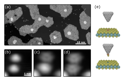
All scanning tunneling microscopy (STM) and spectroscopy (STS) measurements were performed in a UHV low-temperature STM setup with an operating temperature of 6 K. We use Gr on Ir(111) as a substrate. The Ir(111) crystal was first cleaned by cycles of 1.5 keV Ar+ ion beam exposure and annealed to 1550 K. Subsequently, single crystal Gr was grown using the growth method described in Ref. [20]. MoS2 islands were grown according to Ref. [21] using an e-beam evaporator for Mo and a Knudsen cell for sulfur supply. The MoS2 islands were grown at room temperature with a Mo flux of 1.14 1016 , a deposition time of 600 s and a sulfur pressure of 6 10-9 mbar. Afterwards the sample was annealed in a sulfur pressure of 3 10-9 mbar at 1050 K for 300 s, resulting in virtually defect-free single-layer MoS2 islands with small second layer islands on top. Single Fe atom evaporation was performed using an e-beam evaporator at a sample temperature of 8 K. An STM image of the as-grown sample is presented in Fig. 1(a). It becomes apparent, that Fe on MoS2 is non-mobile and does not cluster at low Fe densities.
Sulfur vacancies can be created with high reproducibility by the following procedure: First, the STM tip is positioned over an Fe adatom and approached by decreasing the bias voltage and increasing the tunneling current with closed feedback loop. The tip-adatom separation is reduced until a sudden change in the measured tip height is detected. Typical values are 30 mV and 1 nA. After this event, the tip height is increased to scanning parameters (typically 1 V and I 100 pA). In the large majority of attempts, this procedure creates a sulfur vacancy. A series of STM images showing the subsequent creation of two neighboring sulfur vacancies is presented in Fig. 1(b)-(d).
A model interpreting the observations is shown in Fig. 1(e). The pick-up event involves the adsorbed Fe atom together with a single sulfur atom, leaving a sulfur vacancy in MoS2 behind. While the chemical bond between tip and Fe strongly depends on apex geometry and chemical composition, the Fe-sulfur bond is well defined for every pick-up event. This leads to high reproducibility of the vacancy creation process, as long as the bond between Fe and STM tip is strong enough to initiate the pick-up event. This is in contrast to direct sulfur pick-up events without Fe adatoms reported earlier for bulk MoS2 [22], which we found not to be applicable to single-layer MoS2 islands.
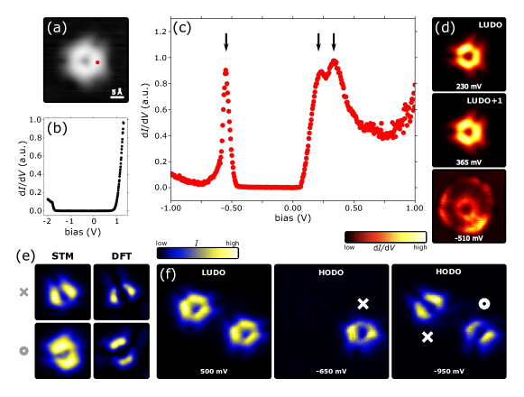
The electronic characterization of an isolated sulfur vacancy created using our atomic manipulation approach is presented in Fig. 2. An STM image of a single vacancy is shown in Fig. 2(a). Its appearance depends on the applied bias voltage, which is discussed in Fig. S1. An STS point spectrum acquired on pristine MoS2 [Fig. 2(b)] displays its band gap [23]. Point spectra taken on the defect lobes reveal the existence of three peaks in the band gap of MoS2, as shown in Fig. 2(c). Corresponding d/d maps measured at the respective peak energies above the Fermi level and presented in Fig. 2(d) show two nearly-equivalent orbitals with C symmetry, the lowest unoccupied defect orbitals LUDO and LUDO+1. In contrast, the d/d map measured close to the peak energy below the Fermi level reveals a modified orbital shape, surrounded by a pronounced ring.
The origin of the peak in the occupied states and the ring in the d/d map is a charging event induced by the STM tip [24]. Applying a bias voltage between tip and sample implies an electric field between them and thus causes the in-gap states of the sulfur vacancy to shift in energy. For large enough negative bias voltages, the LUDO level is pulled below the Fermi energy and occupied by an electron, thus becoming the highest occupied defect orbital (HODO) of the charged vacancy. The peak in the point spectrum of Fig. 2(c) and the ring in the d/d map in Fig. 2(d) at -510 mV thus reflect a sudden change in the occupied defect states due to charging and subsequent distribution of that charge. Similar results have previously been obtained for sulfur vacancies in single-layer WS2 [1].
The absence of additional states in the MoS2 band gap enables us to access the HODO orbital at high bias voltages at which the vacancy is stably charged, by measuring the tunneling current in constant height mode. This signal integrates over all states between the Fermi energy and the bias voltage, which in our system is dominated by the HODO only. Constant-height maps recording the tunneling current are presented in Fig. 2(e). The high-resolution maps reveal two different types of HODOs, denoted as () and (). Both show a clear symmetry reduction from C to C. These orbitals can transform from one to another when neighboring vacancies are charged. This is demonstrated in Fig. 2(f) for two neighboring vacancies. Their LUDOs are measured at 500 mV. At -650 mV, only one of the vacancies is charged, due to differences in the in-gap state energies of the neutral vacancies, displayed in Fig. S2. Hence, only one HODO is observed, in state (). Increasing the bias voltage eventually charges the second vacancy. While the latter is in state (), the other transformed into state ().
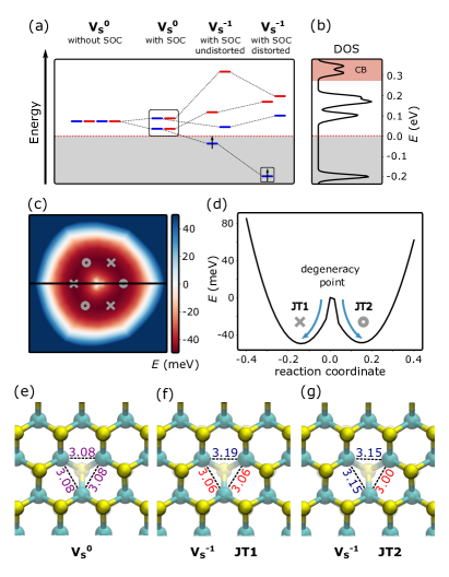
The behavior of the vacancies upon charging can be understood with the help of density functional theory (DFT). For details on the computational methods we refer to the Supplemental Material. Negatively charged sulfur vacancies in MoS2 have been predicted to undergo a JT effect, which distorts the host lattice and spontaneously breaks the (orbital) symmetry from C to C [18, 5, 19]. To understand the JT effect in MoS2 sulfur vacancies, we simulate the energy levels of a MoS2 vacancy, see Fig. 3(a). The three dangling bonds from Mo atoms (, , and ) in symmetry lead to the following symmetry-adapted linear combinations (SALCs): , , and , where belongs to and and to . The lowest state is occupied by two electrons and lies close to the VBM [not shown in Fig. 3(a)]. The two degenerate states are unoccupied and fall in the band gap of MoS2 [25], see Fig. 3(a) (V without SOC). The SALCs can be clearly seen in the charge density plots presented in Fig. S3. Adding SOC partially lifts the degeneracy of the states, leading to two doubly-degenerate levels [Fig. 3(a) (V with SOC)] [26]. These levels correspond to the LUDO and LUDO+1 orbitals found in experiment. Adding an electron to the lowest level lifts all remaining degeneracies, leaving one uncompensated spin below the Fermi energy [Fig. 3(a) (V with SOC undistorted)]. Relaxing the structure spontaneously distorts the atomic configuration around the vacancy, leading to the energy level configuration of the JT effect in negatively charged MoS2 sulfur vacancies, presented in Fig. 3(a) (V with SOC distorted). The corresponding density of states (DOS) is presented in Fig. 3(b). Note that only the HODO is experimentally accessible [solid black box in the level scheme in Fig. 3(a)], since we need to apply a negative bias voltage to charge the vacancy.
Until now theoretical investigations only predicted the existence of one type of JT effect for negatively charged sulfur vacancies in MoS2 [19, 18, 5]. Similarly, a recent experimental work on charged sulfur vacancies in single-layer MoS2 on Gr proposed only one type of distortion to explain the observed orbital symmetry reduction [27]. Our investigations, however, reveal that there are two distinct types of JT distortions, denoted JT1 and JT2. They correspond to two imaginary phonon modes and thus two types of lattice distortions. Both are local minima in the potential energy surface (PES) of the system, which is shown in Fig. 3(c). A direct comparison between our experimental maps and DFT simulations of the HODO, shown in Fig. 2(e), makes plain that the two orbitals denoted by () and () correspond to JT1 and JT2. We thus indicate the local minima of the PES that correspond to JT1 and JT2 by crosses () and circles (), respectively. A cut through the PES along the horizontal line indicated in black, is shown in Fig. 3(d). The JT distortion leads to an energy gain of approximately 50 meV compared to the unrelaxed structure, while JT1 and JT2 distortions have the same energy within the accuracy of our DFT calculation. Upon charging, the sulfur vacancy thus spontaneously transitions into one of the JT distorted states with similar probabilities (blue arrows). The corresponding structural distortions compared to the neutral vacancy configuration [Fig. 3(e)] are shown in Fig. 3(f) and (g). A detailed summary of all simulated JT1 and JT2 orbitals is presented in Fig. S4 and S5.
Coming back to the transformation from JT1 to JT2 shown in Fig. 2(f), we can now infer that it is likely caused by the strain field created when a neighboring vacancy becomes JT distorted. Apparently the elastic energy is minimized, when the two neighboring vacancies are in different JT states.
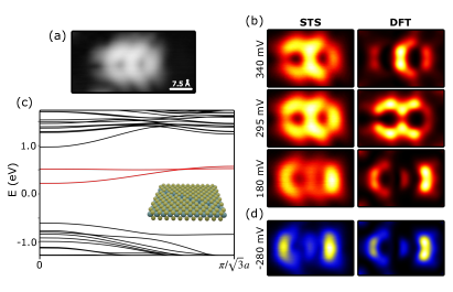
To demonstrate the potential of our vacancy creation technique for the study of larger tailor-made sulfur vacancy structures, we created and characterized a vacancy dimer, see Fig. 4(a). The vacancies are created in next-nearest neighbor distance , with being the MoS2 lattice constant. As can be seen in Fig. 4(b) (left column) the d/d intensity distribution of the hybrid orbitals are distinct from the LUDO and LUDO+1 of isolated vacancies. The observed behavior is reminiscent of bonding and anti-bonding molecular orbitals, which is reproduced in the corresponding DFT maps (right column). Indeed, these hybridized orbitals form two unoccupied bands in a one-dimensional vacancy chain, according to our DFT calculations presented in Fig. 4(c). Such an assembly of large vacancy defect structures can be realized with our atomically precise vacancy creation method, if the adatoms used as markers can be manipulated laterally with sufficiently high fidelity prior to pick-up. While for Fe adatoms on MoS2 the manipulation efficiency is limited, it is plausible that several adatom species exist, which can be laterally manipulated, while simultaneously forming sufficiently strong bonds with the chalcogen atoms to enable pick-up.
Applying a negative bias voltage enables us to charge the dimer. Its HODO is shown in Fig. 4(d), in good agreement with the corresponding DFT simulation for single electron charging. DFT simulations of a doubly charged dimer have a similar appearance, as shown in Fig. S6. The LUDO of the neutral dimer (measured at 180 mV) and the HODO of the charged dimer (measured at -280 mV) have the same shape and hence display no JT distortion, in stark contrast to the spontaneous symmetry breaking observed in the charged single vacancy. This emphasizes the importance of the environment surrounding single vacancies, to enable detection of their pristine properties.
In summary, we have developed a technique for atomically precise creation of point defects in 2D TMDs, involving adsorbed atoms and the tip of an STM. Sulfur vacancies in the top sulfur layer of single-layer MoS2 are created by picking up single Fe adatoms from the surface. Tip-induced gating was used to manipulate sulfur vacancies into a negatively charged state, revealing the existence of two types of JT distortions, which can be transformed into one another by their mutual interaction. Furthermore, we studied the orbital overlap of sulfur vacancy states using the described creation approach and revealed strong hybridization, leading to molecule-like bonding and anti-bonding states.
We acknowledge funding from Deutsche Forschungsgemeinschaft (DFG) through CRC 1238 (project number 277146847, subprojects A01 and B06). J. F. acknowledges financial support from the DFG SPP 2137 (project FI 2624/1-1). H.-P. K. thanks CSC-IT Center for Science Ltd. for generous grants of computer time. A. V. K. acknowledges funding from DFG through project KR 4866/9-1 and the collaborative research center "Chemistry of Synthetic 2D Materials" CRC-1415-417590517.
References
- [1] B. Schuler, D. Y. Qiu, S. Refaely-Abramson, C. Kastl, C. T. Chen, S. Barja, R. J. Koch, D. F. Ogletree, S. Aloni, A. M. Schwartzberg, et al., Phys. Rev. Lett. 123, 076801 (2019).
- [2] G.-J. Zhu, Y.-G. Xu, X.-G. Gong, J.-H. Yang, and B. I. Yakobson, Nano Lett. 21, 6711 (2021).
- [3] G. Zhang, Y. Cheng, J.-P. Chou, and A. Gali, Appl. Phys. Rev. 7, 031308 (2020).
- [4] S. Li, G. Thiering, P. Udvarhelyi, V. Ivády, and A. Gali, Nat. Commun. 13, 1210 (2022).
- [5] S. Gupta, J.-H. Yang, and B. I. Yakobson, Nano Lett. 19, 408 (2018).
- [6] C. Zhang, C. Wang, F. Yang, J.-K. Huang, L.-J. Li, W. Yao, W. Ji, and C.-K. Shih, ACS Nano 13, 1595 (2019).
- [7] K. A. Cochrane, J.-H. Lee, C. Kastl, J. B. Haber, T. Zhang, A. Kozhakhmetov, J. A. Robinson, M. Terrones, J. Repp, J. B. Neaton, et al., Nat. Commun. 12, 7287 (2021).
- [8] S. Trishin, C. Lotze, N. Krane, and K. J. Franke, Phys. Rev. B 108, 165414 (2023).
- [9] B. Schuler, J.-H. Lee, C. Kastl, K. A. Cochrane, C. T. Chen, S. Refaely-Abramson, S. Yuan, E. van Veen, R. Roldán, N. J. Borys, et al., ACS Nano 13, 10520 (2019).
- [10] Y. Zhao, M. Tripathi, K. Čerņevičs, A. Avsar, H. G. Ji, J. F. Gonzalez Marin, C.-Y. Cheon, Z. Wang, O. V. Yazyev, and A. Kis, Nat. Commun. 14, 44 (2023).
- [11] W. Zhou, X. Zou, S. Najmaei, Z. Liu, Y. Shi, J. Kong, J. Lou, P. M. Ajayan, B. I. Yakobson, and J.-C. Idrobo, Nano Lett. 13, 2615 (2013).
- [12] H.-P. Komsa, S. Kurasch, O. Lehtinen, U. Kaiser, and A. V. Krasheninnikov, Phys. Rev. B 88, 035301 (2013).
- [13] J. Hong, Z. Hu, M. Probert, K. Li, D. Lv, X. Yang, L. Gu, N. Mao, Q. Feng, L. Xie, et al., Nat. Commun. 6, 6293 (2015).
- [14] E. Mitterreiter, B. Schuler, K. A. Cochrane, U. Wurstbauer, A. Weber-Bargioni, C. Kastl, and A. W. Holleitner, Nano Lett. 20, 4437 (2020).
- [15] P. Valerius, S. Kretschmer, B. V. Senkovskiy, S. Wu, J. Hall, A. Herman, N. Ehlen, M. Ghorbani-Asl, A. Grüneis, A. V. Krasheninnikov, et al., 2D Mater. 7, 025005 (2020).
- [16] B. Ozden, T. Zhang, M. Liu, A. Fest, D. A. Pearson, E. Khan, S. Uprety, J. E. Razon, J. Cherry, K. Fujisawa, et al., ACS Nano 17, 25101 (2023).
- [17] H. Fang, H. Mahalingam, X. Li, X. Han, Z. Qiu, Y. Han, K. Noori, D. Dulal, H. Chen, P. Lyu, et al., Nat. Nanotechnol. 18, 1401 (2023).
- [18] H.-P. Komsa and A. V. Krasheninnikov, Phys. Rev. B 91, 125304 (2015).
- [19] A. M. Z. Tan, C. Freysoldt, and R. G. Hennig, Phys. Rev. Mater. 4, 064004 (2020).
- [20] A. T. N’Diaye, J. Coraux, T. N. Plasa, C. Busse, T. Michely, et al., New J. Phys. 10, 043033 (2008).
- [21] J. Hall, B. Pielić, C. Murray, W. Jolie, T. Wekking, C. Busse, M. Kralj, and T. Michely, 2D Mater. 5, 025005 (2018).
- [22] S. Hosoki, S. Hosaka, and T. Hasegawa, Appl. Surf. Sci. 60, 643 (1992).
- [23] C. Murray, W. Jolie, J. A. Fischer, J. Hall, C. van Efferen, N. Ehlen, A. Grüneis, C. Busse, and T. Michely, Phys. Rev. B 99, 115434 (2019).
- [24] N. A. Pradhan, N. Liu, C. Silien, and W. Ho, Phys. Rev. Lett. 94, 076801 (2005).
- [25] M. Pandey, F. A. Rasmussen, K. Kuhar, T. Olsen, K. W. Jacobsen, and K. S. Thygesen, Nano Lett. 16, 2234 (2016).
- [26] M. A. Khan, M. Erementchouk, J. Hendrickson, and M. N. Leuenberger, Physical Review B 95, 245435 (2017).
- [27] F. Xiang, L. Huberich, P. A. Vargas, R. Torsi, J. Allerbeck, A. M. Z. Tan, C. Dong, P. Ruffieux, R. Fasel, O. Gröning, et al., arXiv preprint arXiv:2308.02201 (2023).