Switching plane: A novel crystalline interface in orthorhombic perovskite films
Abstract
The atomic configuration of phases and their interfaces is fundamental to materials design and engineering. Here, we unveil a novel crystalline interface, whose formation is driven by energetic influences that compete in determining the orientation of an orthorhombic perovskite film. Observed within LaVO3 grown on DyScO3, the film resolves this competition by switching its orientation at an atomically-flat plane within its volume, not at the film–substrate interface. Remarkably, at either side of this switching plane, characteristic orthorhombic distortions tend to zero to couple mismatched atomic structures. The resulting boundary is highly energetic; by using second-principles modeling to map the phase space of film growth, we show how its formation requires structural relaxation of an entire film grown beyond a significant critical thickness. This structural–energetic phenomenon opens avenues towards engineering new functional interfaces, offering the opportunity of contacting distinct phases of one compound that would never otherwise coexist.
I Main
In any crystalline material, interfaces help define the physical properties, whether mechanical, electronic, magnetic or optical sutton1995interfaces . Because of their importance, determining and understanding the nature of crystalline interfaces remains a vital area of research, even for well-established categories such as grain boundaries in metals or domain walls in ferroelectric thin films Meiners2020 ; FDW . Here, we report a new type of structural interface, termed the switching plane. Formed within a chemically-uniform transition metal oxide (TMO) film, it corresponds to an atomically-thin boundary where its Pnma perovskite lattice switches orientation by 90°. In TMO materials, it is widely known that interfaces can be exploited to create functional properties beyond the scope offered by the unbound crystal, such as the formation of a two-dimensional electron system at the interface between insulating LaAlO3 and SrTiO3 compounds Ohtomo2004 . Within single-phase compounds, crystalline boundaries such as domain walls in ferroelectric or ferroelastic materials have themselves produced emergent properties distinct from their bulk counterparts Tagantsev2010 ; Langenberg2019 ; Farokhipoor2014 . In comparison to these priors, as well as introducing a new paradigm for interface energetics and formation, the switching plane opens unique opportunities for the deterministic engineering of novel functional properties.
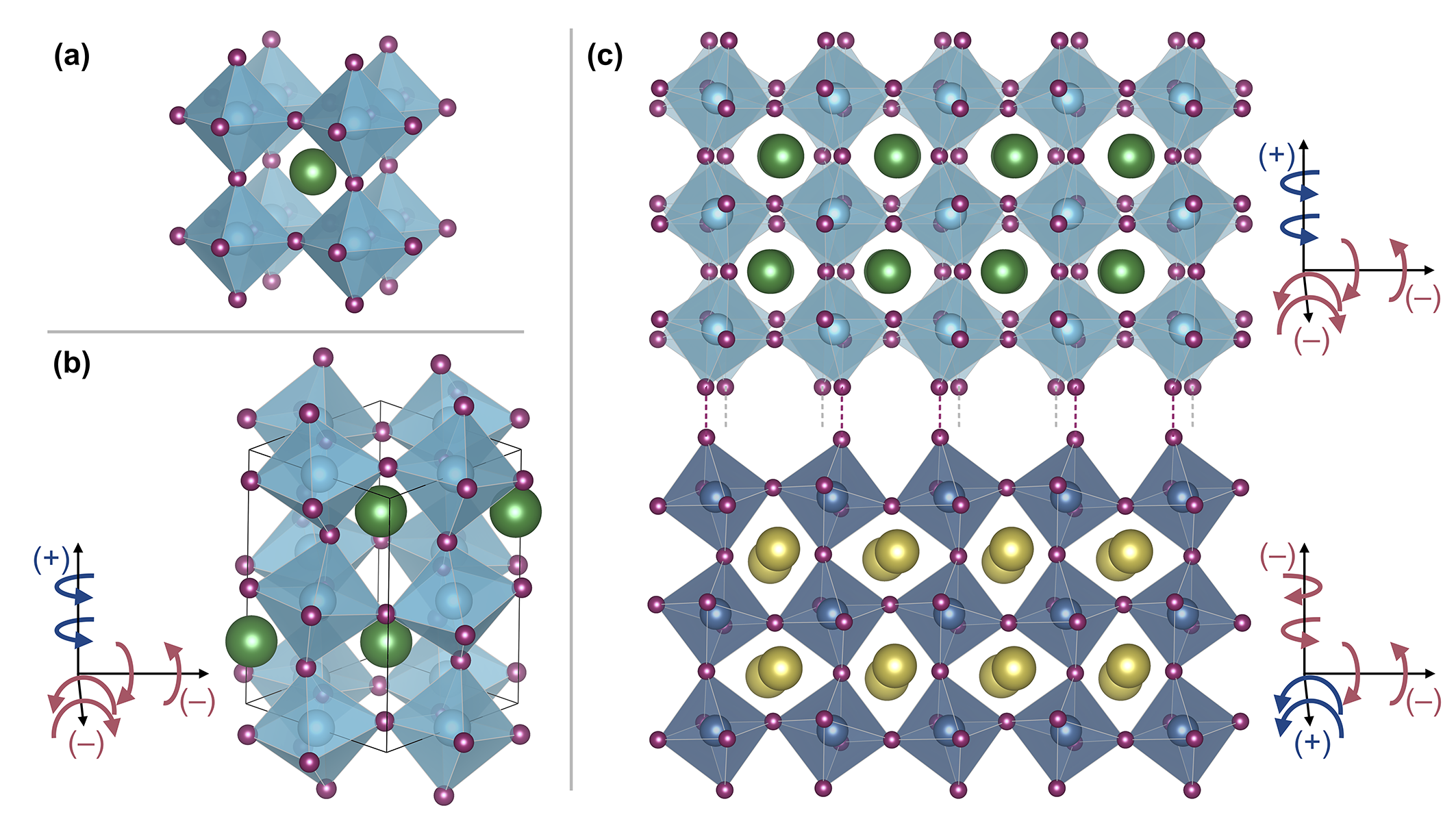
The phenomenon we report takes as starting point the ABO3 perovskite, Fig. 1(a), in its most common structural form: orthorhombic, Fig. 1(b)) Woodward1997 . Specifically, we impose a structural conundrum during epitaxial growth of an orthorhombic film, by depositing it on a substrate which applies boundary conditions that induce two opposing energetic influences on the film’s orientation. The first influence comes from growing the film under biaxial epitaxial tension. In the absence of strain-relieving defects, the resulting macroscopic strain energy is minimized by the film’s orthorhombic long axis ( for Pnma space group) orienting perpendicular to the substrate plane (“out-of-plane”); see Masset2020 ; Choquette2016 ; Rotella2012 ; Meley2018 ; Meley2019 ; Mundet2023 . The second influence derives from the local atomic topography of the substrate, which is also selected as orthorhombic perovskite. We can consider the rotations of its oxygen octahedra along pseudocubic axes of type . On the pseudocubic axis parallel to , the octahedra rotate in-phase, while they rotate out-of-phase on the two axes inhabiting the plane (Fig. 1(b), Supplementary Fig. 1). Therefore, by choosing a substrate orientation – where is in-plane – the substrate’s oxygen octahedra rotate in-phase along one in-plane pseudocubic axis and out-of-phase along the other one. (On the out-of-plane pseudocubic axis, rotations are out-of-phase.) In contrast, for a film having out-of-plane – the orientation favored for biaxial tensile strain – the octahedra follow an out-of-phase configuration along both of the in-plane pseudocubic axes. As shown in Figure 1(c), the oxygen octahedra rotations (OOR) of these two structures do not match, creating a connectivity problem. Combining this OOR connectivity mismatch with the macroscopic tensile strain state leads, in some parameter range, to the new and unique switching plane.
To develop a basis for understanding switching plane formation, in Fig. 2 we first explore the consequence of OOR mismatch on a 52 pseudocubic unit cell (uc) thick LaVO3 film grown, by pulsed laser deposition, under % biaxial tension on a DyScO3 substrate (see Supplementary Table 1). Fig. 1(b) shows a scanning transmission electron microscopy (STEM) image of the sample, recorded on the / zone axis of the substrate. Using the atomic number contrast of the high angle annular dark field (HAADF) detector, it depicts the brighter -site and darker -site cations. This enables imaging of a characteristic distortion of the orthorhombic perovskite lattice, namely the “” mode, consisting of an antipolar motion (AM) of the -site cations, such that they adopt positive and negative displacements along the axis when following a lattice vector parallel to (Supplementary Fig. 1). Since, in the substrate, lies in-plane, in Fig. 2(a) its mode is seen in projection as a vertical AM of successive layers of -site cations. We emphasize that, because of a trilinear energetic term coupling AM with both types of OOR, visualization of this mode can be used as a proxy for determining the in-phase OOR axis and relative amplitude Zhang2013 ; Moon2014NC ; Meley2018 ; Dominguez2020 . Fig. 2(a) shows that the up–down AM propagates across the entire LaVO3 film. This is because the energetic cost of coupling the mismatched OOR of the strain-state favored film with those of the substrate is sufficiently high that the film has instead adopted the symmetry and rotation configuration of the substrate, keeping in-plane. As confirmation, quantified maps of the -site cation positions in Fig. 2(b) and (c) show that their projected AM remains purely in the out-of-plane pseudocubic direction across the film. The quantified line profile Fig. 2(d) in turn shows that the magnitude of displacement decays over 8 uc from substrate into film, while the continuity of in-phase OOR from substrate into film is confirmed by annular bright field (ABF) STEM imaging around the film–substrate interface (Supplementary Fig. 2).
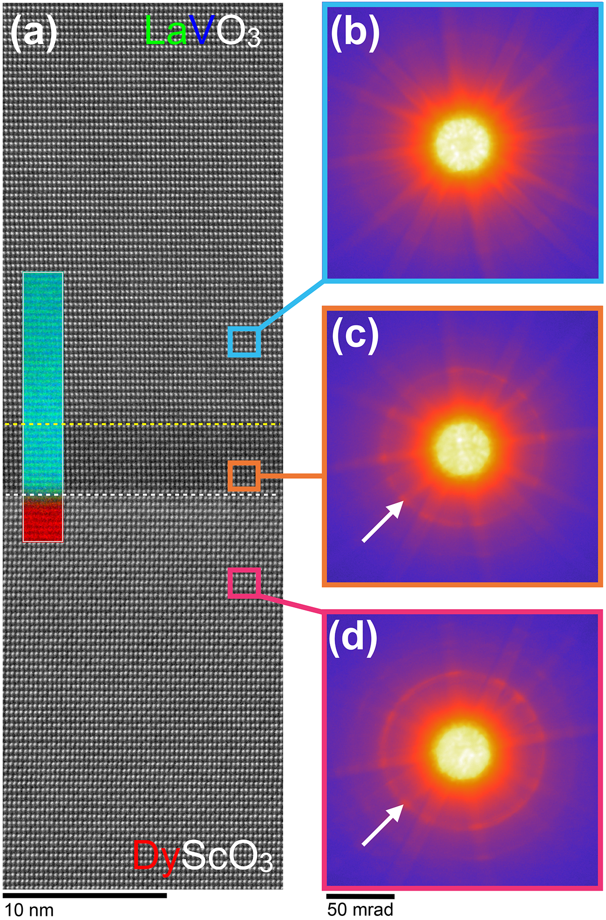
Similar imposition of substrate symmetry and rotations has been observed previously, in analogous / film/substrate combinations, for films up to 35–40 uc thickness Proffit2008 ; Liao2016AFM ; Yuan2018 ; Choquette2016 ; Mundet2023 . (Alternative symmetry imposition, where a cubic substrate suppresses the out-of-phase OOR of a rhombohedral compound, has also been observed in ultrathin 5 uc LaCoO3 films grown on SrTiO3 Qiao2015 .) Nevertheless, such a film has an increased macroscopic strain energy over one having out-of-plane; a strain energy that scales with film thickness. Therefore, one may ask, if film growth is continued, is there a critical thickness at which an epitaxial orientation transition will be induced? That is, a thickness at which the energetic gain from the film adopting out-of-plane is enough to force the creation of an interface that couples the mismatched OOR of substrate and bulk film? As a first step in looking at this question, Fig. 3(a) shows a lower magnification HAADF STEM image of a much thicker LaVO3 film. As established before Meley2018 , the bulk lattice orientation of this film actually is determined by the biaxial tensile strain, with out-of-plane. Structurally, therefore, the mismatched OOR of bulk film and substrate must have been accommodated. This image, recorded on the ( DyScO3) zone axis, provides a first hint at this accommodation, from a band of darker contrast 10 uc thick that lies within the film, running along the film–substrate interface. Compositional analysis finds that this darker contrast is not chemical in origin (Fig. 3(a), Supplementary Figs. 3, 4). It is instead structural, as indicated by the accompanying position averaged convergent beam electron diffraction (PACBED) patterns of Figs. 2(b)–(d).
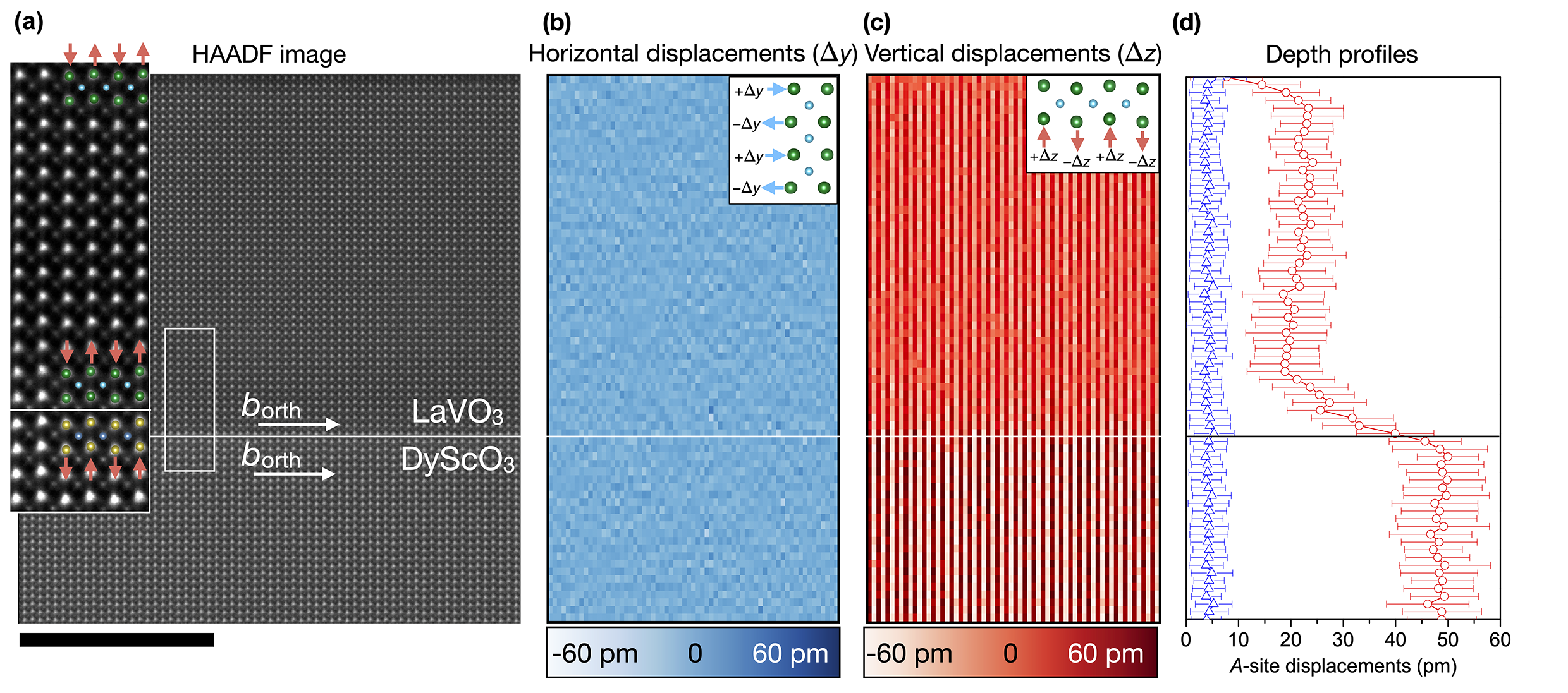
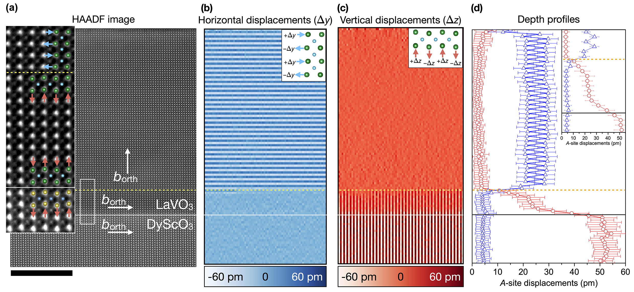
We now study this structural formation in more detail, in an 81 uc thick film. We use HAADF STEM imaging on the / zone axis of the substrate to evaluate the -site AM of the orthorhombic lattices. Compared to the alternative approach of “direct” imaging of in-phase rotations using, for instance, ABF, this enables measurement of the orthorhombic distortions of both in-plane and out-of-plane in a single image. It is further robust to residual aberrations and sample mis-tilts, such that quantitative atomic data can be taken across the entire 35 nm thickness of the film, with a 4k4k pixel resolution. Fig. 4(a) presents an example image. In the DyScO3 substrate at the bottom of the zoomed inset, the -site cations have an up–down AM for in-plane. In contrast, higher up in the LaVO3 film they displace left–right, indicating that it has adopted out-of-plane, as favored by tensile strain. Surprisingly, however, the transition between these two orientations does not occur at the film–substrate interface. Instead, the AM of the substrate propagates into the film over 10 uc, and only then switches orientation. In Fig. 4(b) and (c), this observation is studied with quantified maps of -site left–right () and up–down () displacements. In a segment that we term the intermediate layer (IL), the AM of the substrate continues into the LaVO3, before a sharp segue to the left–right AM of the film bulk. Fig. 4(d) shows depth profiles of the average -site displacements across the IL. Going from the substrate into the thin film, the projected AM displacements remain purely parallel to the pseudocubic -axis. At the same time, their amplitude decays over a few unit cells to a plateau of 5 uc length. At the end of this, the amplitude further decays rapidly, reaching a value near zero at the top of the IL. At this point – which we term the switching plane – projected AM displacements switch sharply to being parallel to the pseudocubic axis, corresponding to an out-of-plane . The displacements then increase in amplitude over a few uc to reach their final value for the bulk film structure. The amplitude of AM in the IL plateau region is approximately equal to that of the film’s bulk structure. In agreement with this analysis, ABF STEM along substrate shows directly how the in-phase OOR of the IL tend to zero at the switching plane (Supplementary Fig. 5).
The initial continuity of substrate symmetry into the film over some 10 uc, followed by a switch to out-of-plane, explains the PACBED results along in Fig. 3. The corresponding zone axis of the DyScO3 substrate gives it a strong first order Laue zone (FOLZ) ring at a low scattering angle of 60 mrad, owing to a symmetry distance doubling along the beam path direction Nord2019 . Because of the structural continuity, this FOLZ ring remains in the IL; however, it disappears in the film bulk when the zone axis switches to . 4D-STEM proves that this disappearance occurs discretely, when stepping one uc across the switching plane (Supplementary Fig. 6). Together with simulations using STEM Forbes2010 ; MuSTEM , the PACBED analysis also explains the darker contrast from the IL in Fig. 3(a). Specifically, this arises from strong elastic scattering into the FOLZ rings of the substrate and IL that consequently leads to them having anomalously low thermal diffuse scattering and hence decreased signal on the HAADF detector (Supplementary Figs 7, 8). As a result, the dark contrast along the zone axis itself constitutes an indication of IL/switching plane formation.
To summarize, thicker LaVO3 films adopt the orientation expected from the substrate-imposed tensile strain, except for an initial IL which keeps the substrate orientation. The switch between the two orientations occurs sharply, at the switching plane. As described later, the local atomic topography at the switching plane enables a subtle transition between the mismatched OOR of the bulk film and substrate orientations. Associated with this, incompatible orthorhombic distortions tend to a value of zero, while compatible ones propagate freely. Since it contains strong local distortions compared to the structure that forms the basis of the LaVO3 lattice, this novel interface is a highly energetic boundary.
Our findings have various implications. First, the critical thickness for transitioning to the strain-state determined bulk film orientation, tied to switching plane and IL formation, is clearly between 52 and 81 uc. By using X-ray diffraction to monitor the appearance of a half-order reflection for out-of-plane in a film thickness series, this value is further narrowed to between 60 and 74 uc (Supplementary Fig. 9). Second, given that, during deposition, the film initially grows in structural continuity with the substrate, its atomic lattice must dynamically restructure after reaching the critical thickness, when the bulk film switches its orientation. While the required energy for restructuring is presumed to be thermal from the substrate heating, the mechanism remains an open question. Finally, we hypothesize that the switching plane combined with IL represent an energetic minimum, as compared to forming an OOR-coupled interface that coincides with the film–substrate interface. This reminds of the stand-off effect of misfit dislocations, where the origin of the strain-releasing defects sits in the elastically weaker material, a few uc far from the layer–substrate interface Mader1991 ; Gutkin1994 ; Lu2019 . Given its importance, we now explore the energetics of the system via second-principles calculations.
Making appropriate simulations is a non-trivial task, owing to the need to include tens of uc thickness in the film. The “standard” approach of density functional theory calculations, as for instance used to calculate the biaxial strain determined LaVO3 structure Meley2018 , is therefore unviable. In order to address this challenge, we innovate a second-principles modeling approach Schmitt2020th ; Ghosez22 . For both tractability and universality, we work with the prototypical orthorhombic system of CaTiO3, which we adapt to incorporate physics and constraints analogous to our experimental system. We emphasize that the second-principles model is validated by comparison to first principles results; see Schmitt2020th ; Zhang2023 and Supplementary Fig. 10.
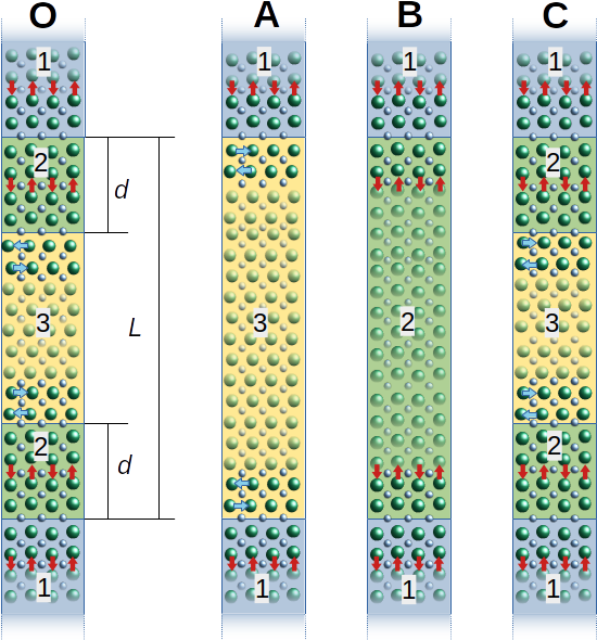
The atomic structure “O” in Fig. 5 defines the basic supercell setup for the simulations. It makes use of periodic boundary conditions that duplicate the interface. Segment 1 mimics the atomic environment created by the substrate: it is a region of Pnma structure with in-plane, in which the orthorhombic distortions (OOR and -site AM) are artificially-amplified and frozen to replicate the distortion mismatch and biaxial strain imposed by the substrate at the LaVO3–DyScO3 interface. Segments 2 and 3 comprise the thin film. To represent the IL, segment 2 has a Pnma structure with in-plane, while segment 3 conforms to the out-of-plane structure. Simulations are made for a series of values of absolute film thickness , as specified in uc layers. For each , we consider the energies of the three configuration types illustrated in Fig. 5: A) film of energy that consists only of out-of-plane (); B) film of energy that consists only of in-plane (); C) films of energies containing a mix of both orientations with IL thickness (). Each structure in the sequence of is allowed to relax (atomic positions in segments 2 and 3 and cell parameter out-of-plane), after which their energetic values are compared.
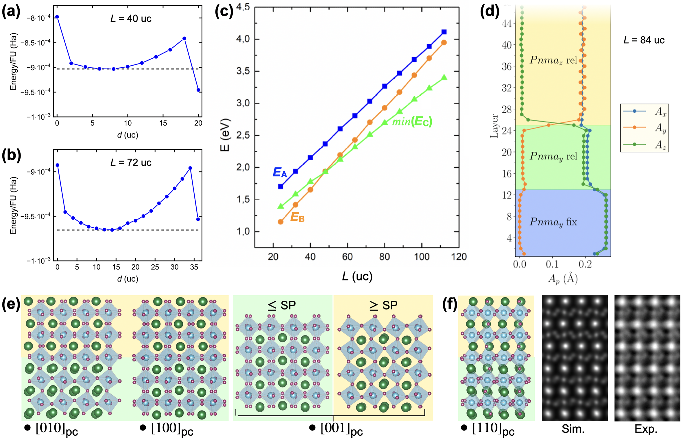
From the simulation results, Fig. 6(a) presents the energetic evolution of a relatively thin film (), in function of . The highest energy is observed for , which corresponds to placing the switching plane at the film–substrate interface (configuration A). As increases, the energy decreases to a minimum at , but then rises again. Finally, for , the curve shows a sharp decrease to its lowest energy, making B the most favorable configuration; i.e., the symmetry-imposed structure, as for LaVO3 films under critical thickness. Considering the results for a thicker film with in Fig. 6(b), a similar curve is seen. However, there is one key difference: the minimum energy in the initial concave (at ) is now lower than that of the final, sharp minimum at . Therefore, configuration C having an IL and implicit switching plane is now the most energetically favorable. By repeating the calculations for (Supplementary Fig. 11), the summarizing plot in Fig. 5(c) is determined, in which corresponds to the minimum by adjusting to an optimized value for each . Remarkably, the second-principles simulations reproduce the experimentally-observed transition, since the lowest energy configuration changes from configuration B with uniformly in-plane to the mixed in-plane/out-of-plane configuration C at a critical film thickness of, in this case, uc. Since configuration A is never favored, the model therefore proves that some structural relaxation is needed within the film in order to reduce the energy of the switching plane and hence enable its formation. While these energetics push the switching plane away from the film–substrate interface, pushing the other way is the energetic compensation from maximising the volume of film with out-of-plane, such that the switching plane adapts an “equilibrium” position at distance from the film–substrate interface. Supplementary Note 1 provides a more detailed physical description of the energetics.
Fig. 6(d) plots depth profiles of the -site AM amplitudes for the configuration of an example film above the critical thickness. and are respectively equivalent to the and values measured along the zone axis in Figs. 2 and 4. At the film–substrate interface, the amplitude of the substrate AM propagates into the film, but decays over 2–3 uc to a 10 uc plateau. At the end of the plateau, sharply decays towards zero amplitude at the switching plane. At that point, the amplitude of sharply increases from zero to that of the bulk thin film structure of segment 3. These AM transitions mirror those measured for the LaVO3/DyScO3 system in Fig. 4, vindicating the similarity of model to experiments. Notably, the AM amplitude modulation across the switching plane occurs much more sharply than that at the film–substrate interface in films grown below the critical thickness, where the substrate symmetry is preserved (see Fig. 2). This can be understood as the system confining the distorted and highly energetic structure around the switching plane to a small volume for energetic minimisation.
Interrogation of the structural model, and its comparison to STEM data along different zone axes, allow us to elucidate further the nature of atomic structure transition across the switching plane. Fig. 6(e) shows projections of the structural model on the three pseudocubic axes. is projected along the axis of the substrate, and illustrates how the mismatched OOR of bulk film and substrate interface by a sharp flattening or damping within 2 uc either side of the switching plane. Along , as well as AM we visualize out-of-phase OOR modes for both substrate and bulk film orientations. These two modes do not face the same connectivity problem and, because of this compatibility, we see that the mode propagates undamped across the switching plane. Experimental ABF STEM data are consistent with this finding; see Supplementary Fig. 12. In order to study OOR connectivity on the out-of-plane axis, we present two projected slices, each 2 uc thick: one that includes the switching plane uc and the uc below ( SP) and the other including the switching plane uc and the uc above ( SP). It is evident that, on this axis, the OOR mode switches from out-of-phase to in-phase very sharply, with negligible damping. Such an abrupt switching in OOR modes along the out-of-plane axis has previously been seen in rhombohedral/orthorhombic heterostructures He2015 , and occurs because the apical oxygen effectively acts as a free pivot point for out-of-plane rotations. In a cross-section sample, these rotations can be monitored by measuring the symmetry of O dumbbells or clusters imaged on a axis He2015 . Fig. 6(f) shows the appropriate projection, where the bulk film has a zone axis. Above the switching plane, the O dumbbells are mirrored by a horizontal plane – indicative of in-phase OOR along the out-of-plane axis. Below it, as the OOR go to out-of-phase, the O clusters lose this mirror symmetry. From the model, an (inverted) ABF image is simulated (“Sim.”), substituting the Ca and Ti cations by La and V respectively, in order to be more easily compared to the experimental data. The experimental image (“Exp.”) on the right bears a remarkable resemblance to the simulation, supporting the simulation-based hypothesis that out-of-plane OOR switch directly from out-of-phase to in-phase across the switching plane.
In summary, through experiments and simulations, we have revealed a complex “phase space” for guiding the design choice of orthorhombic film growth, set by factors of epitaxial strain, OOR connectivity and film thickness. As shown by simulations in Fig. 6, under our chosen / parameters, films grown below a critical thickness have a structural phase set by OOR connectivity. Above the critical thickness, the film instead adopts a two phase structure: a bulk structure set by epitaxial strain, and a thin IL adjacent to the substrate which instead follows the substrate orientation. The calculations further show that considering only the epitaxial strain in OOR/strain imposed systems ( Meley2018 ; Zhang2022 ) gives the highest film energy of all structural variants, and so does not correctly predict the film’s complete atomic structure.
In films grown beyond the critical thickness, the switching plane is formed between the two phases of the film, itself representing a new paradigm in crystalline interface formation. Its formation is driven solely by energetics, with no stochastic role of grain or domain nucleation. One consequence is that it appropriates the atomic flatness of the substrate, as for instance seen by the switching plane mirroring the substrate step edge in Fig. 4. Simulations nevertheless imply that the IL thickness derives from a broad energetic minimum (see energetic curves in Fig. 6b and Supplementary Fig. 11). The exact IL thickness is therefore expected to be sensitive to subtle factors during switching plane formation. This could explain small differences in IL thickness that are sometimes observed at different sampling points for a single deposited film, and is an aspect we are investigating with further experiments. While the atomic landscape of the IL and switching plane is confined to a relatively short length-scale of some 10–15 uc, it is a consequence of energetics acting over the entire film, grown beyond a significant critical thickness of tens of uc. Indeed, its formation can only be predicted by including the film’s full atomic structure in a simulation. Because of this subtlety, conceivably its presence has been missed in previous work Kan2013 .
The switching plane separates two regions of the same chemical compound (IL and film bulk) that are held under distinct mechanical boundary conditions. Because it is induced by simple opposition of energetic influences on epitaxial film growth, it is in principle applicable to other Pnma/Pnma film/substrate combinations. Given that the orthorhombic lattice is the most common TMO perovskite structure Woodward1997 , this gives a wide potential for creating the IL and switching plane in other compounds. Two candidates are manganite or nickelate films. In these, we can exploit the different strain conditions of the IL and bulk film to engineer adjacent regions that, despite being of the same compound, have distinct electronic and magnetic properties, with the switching plane forming an unprecedentedly sharp interface between them. The IL of such a structure could, for instance, be used to pin the magnetic phase in a LaMnO3 film grown on GdScO3 to the reorientation, thus forming a chemically-uniform material that is magnetically inhomogeneous Schmitt2020 . The recent observation of structural variations in La2/3Ca1/3MnO3 films subject to an alternative configuration of substrate-imposed strain and OOR connectivity Zhang2022 supports the feasibility of engineering the switching plane in manganite heterostructures. Other possibilities for engineering novel functional properties also open up, such as leveraging this atomically-flat interface to create a 2-dimensional conductor Catalan2012 . Assuming the ideality of a purely energetic construct, free of stochastic influences, the formation of these conceptions should also be deterministic, thereby enabling materials-by-design at a fundamental level Olson2000 ; Alberi2018 .
II Acknowledgments
This work was supported by the Swiss National Science Foundation – division II – projects 200020-179155 and 200020-207338, by the Synergia Project N. 154410, and has received funding from the European Research Council under the European Union Seventh Framework Programme (FP7/2007–2013)/ERC Grant Agreement n.319286 (Q-MAC). P.G. acknowledges financial support from F.R.S.-FNRS Belgium (grant PROMOSPAN) and the European Union’s Horizon 2020 research and innovation program under grant agreement number 964931 (TSAR). Calculations were performed on the CECI supercomputer facilities funded by the FRS-FNRS (Grant No. 2.5020.1), the Tier-1 supercomputer of the Fédération Wallonie-Bruxelles funded by the Walloon Region (Grant No. 1117545), and the computing facilities of the Flemish Supercomputer Center. The CIME at EPFL is thanked for access to electron microscope facilities. Cécile Hébert/LSME of the IPHYS, EPFL are thanked for continued support of D.T.L.A, and for hosting B.M. during much of this work. We thank Jinhui Guo for assistance with plotting PACBED experimental and simulated data, and Clémentine Thibault and Chih-Ying Hsu for useful discussions.
III Author contributions
H.M. fabricated the heterostructures and carried out the X-ray diffraction measurements with S.G. STEM measurements were performed and analysed by D.T.L.A. with B.M. The second-principles model was developed by M.S. and P.G. D.T.L.A., S.G. and P.G. wrote the manuscript with input from all the authors. All the authors contributed to the analysis and interpretation of the experimental results.
IV Methods
Thin film growth
The LaVO3 films are grown on DyScO3 substrates by pulsed laser deposition using an excimer KrF laser run at 1 Hz repetition rate and at high pulse fluence (2 J/cm2). Deposition occurs on substrates heated from 800∘ C to 900∘ C (standard value of 880∘ C) in a mbar oxygen atmosphere from a ceramic target of LaVO4; cooling is performed under the same oxygen pressure. In situ reflection high energy electron diffraction reveals that the deposition evolves from a layer-by-layer growth mode during the first few unit cells to a mainly step-flow mode. Atomic force microscopy identifies the high surface quality of the films: the film topography for all the thicknesses displays a step-and-terrace structure, mirroring the DyScO3 substrate surface. For more details, see reference Meley2019 .
X-ray diffraction
The scans were acquired with a X’Pert PRO PanAlytical diffractometer equipped with a Ge(220) monochromator and a triple-axis analyzer.
Scanning Transmission Electron Microscopy
Samples for STEM were prepared either by a combination of mechanical polishing using an Allied High Tech MultiTech polishing system, followed by argon ion beam milling with a Gatan PIPS II system to electron transparency, or by focused ion beam milling using a Zeiss NVision 40. All STEM data were acquired using a monochromated, double aberration-corrected FEI Titan Themis 60-300 operated at a high tension of 300 kV and using a probe semi-angle of convergence of 20.7 mrad and beam current of 40 pA. HAADF STEM images were acquired using a Fischione photomultiplier tube (PMT) detector. Unless otherwise stated, detector collection semi-angles of 50–200 mrad were applied, using a nominal camera length of 115 mm. For quantitative analysis of atomic column positions, image stacks were recorded at 90∘ rotations between consecutive frames. These stacks then underwent rigid and non-rigid alignment using the SmartAlign software Jones2015 , in order to reduce artefacts from system noise and scan drift. In order to decouple scan distortions from the atomic column row directions, the images were acquired with an angle of 10–15∘ between the fast scan direction and one of the principal directions of the atomic rows. This methodology was successfully applied for frames up to 4k 4k pixels in size. In the HAADF images, and cation positions were identified by fitting two-dimensional Gaussian functions using Atomap Nord2017 . From these measurements, quantified maps and averaged depth profiles of and AM displacements were calculated using custom Python scripts.
When ABF images were recorded to visualize O sites, these were acquired simultaneously to the HAADF image series with the same nominal 115 mm camera length, using a Gatan PMT detector mounted at the entrance of a Gatan GIF Quantum ERS, giving collection semi-angles of 10.6–24.3 mrad. Scan distortions were corrected by first performing rigid and non-rigid alignment of the HAADF image stack, and then applying the HAADF-determined corrections to the simultaneously-acquired ABF image stack. In this way, the rigid and non-rigid alignment is unaffected by distortions from residual aberrations, sample mis-tilts or improper defocus that can have a stronger effect on the phase-contrast ABF image than incoherent HAADF image. O column positions were similarly identified using Atomap, with —O— angle plots calculated using a custom Python script. Sub-frame averaging was performed with the SmartAlign Template Matching Module.
Analytical data were acquired using the same instrument, with STEM-EELS maps recorded with the Gatan GIF Quantum ERS, and energy-dispersive X-ray spectroscopy (EDXS) data recorded using the FEI/Thermo Fisher Scientific ChemiSTEM 4 quadrant silicon drift detector system. The EDXS data were recorded using the same probe semi-angle of convergence and HAADF detector set up as previously described. In contrast, the EELS data were recorded using a monochromated setup, with a probe semi-angle of convergence of 18 mrad, spectrometer semi-angle of collection of 36 mrad, and HAADF angles of 74–170 mrad. The STEM-EELS elemental maps were prepared using the analysis functions in Gatan DigitalMicrograph 3.5. Note that the V map of Fig. 3 and Supplementary Fig. 3 was integrated only from the V peaks, in order to avoid contribution from the O -edge. STEM-EDXS chemical maps and line profiles were prepared using Thermo Fisher Scientific Velox 3.10 software, applying a Schreiber-Wims ionization cross-section model for elemental quantification.
PACBED patterns were acquired in two different ways. The PACBED data presented in the main text were acquired using the Gatan Ultrascan CCD camera of the GIF. The PACBED data presented in Supplementary Fig. 6 were acquired using a MerlinEM (Quantum Detectors) Medipix3. For this latter measurement, the microscope was operated at 200 kV high tension.
STEM image simulations were performed with Dr. Probe software Barthel2018 , using the imaging conditions detailed above for experimental acquisition, with aberrations and defocus set to 0. A source size of 0.015 nm was applied. PACBED simulations were performed using STEM MuSTEM .
Second-principle calculations
A second-principles model of CaTiO3 was used to perform structural relaxations with applied constraints, as described in the main text, mimicking the conditions exhibited by the LaVO3 thin film grown on the DyScO3 substrate. Relaxations were performed using supercell sizes up to repetition of the 5-atom pseudocubic perovskite structure (9920 atoms). The atomic relaxations were performed using the Multibinit package GONZE2020 , until the maximum force become smaller than .
The second-principles model was built with the Multibinit package which implements the second-principles approach outlined in references Wojdel2013 and Escorihuela-Sayalero2017 . This method relies on a Taylor expansion of the potential energy surface (PES) around the reference cubic structure in terms of all structural degrees of freedom, with coefficients then determined from first-principles data. In this scheme, the energy includes harmonic and anharmonic contributions in terms of individual atomic displacements, macroscopic strains and their couplings, with the long-range dipole-dipole interaction treated explicitly. At the harmonic level, the coefficients are exactly those directly computed from density functional perturbation theory. At the anharmonic level, the most relevant terms are selected and their coefficients are fitted in order to reproduce the energies, forces and stresses computed from density functional theory (DFT) for a set of configurations properly sampling the PES.
The training set of first-principles DFT data contained more than 5000 structures, calculated with the Abinit software package, making used of a plane-wave pseudopotential approach Gonze2002 ; Gonze2009 ; Gonze2016 ; GONZE2020 . The DFT calculations were performed within the generalized gradient approximation making use of the Wu-Cohen parametrization Wu2006 , that was further checked Zhang2023 to provide results totally comparable to PBEsol Perdew2008 . The plane wave energy cutoff was of 40 Ha, and the Brillouin zone sampling equivalent to a grid for the 5-atom perovskite cubic uc. The final effective atomic potential contains 360 polynomial terms, until order 8 and was further validated by comparison with first-principles data. It describes well the relative phase stability and distortion amplitudes of the most important metastable phases of CaTiO3. It accurately reproduces the phonon dispersion curves of its ground state and captures its temperature behavior. It further reproduces the atomic relaxation at ferroelastic twin walls, reproducing results previously obtained from first-principles by Barone et al. Barone2014 ; see Supplementary Fig. 10. Exhaustive details on the construction of the second-principles model of CaTiO3 and of its validation by comparison to first-principles calculations, are provided in reference Schmitt2020th .
V Data availability
The data that support the findings of this study are available from the corresponding author upon reasonable request.
VI Code availability
The computer codes and algorithms used to generate the results reported in the article are available from the corresponding author upon reasonable request.
References
- (1) Sutton, A. & Balluffi, R. Interfaces in Crystalline Materials. Oxford Classic Texts in the Physical Sciences (OUP Oxford, 1995).
- (2) Meiners, T., Frolov, T., Rudd, R. E., Dehm, G. & Liebscher, C. H. Observations of grain-boundary phase transformations in an elemental metal. Nature 579, 375–378 (2020). URL https://doi.org/10.1038/s41586-020-2082-6.
- (3) Meier, D., Seidel, J., Gregg, M. & Ramesh, R. (eds.) Domain walls (Oxford University Press, 2020).
- (4) Ohtomo, A. & Hwang, H. Y. A high-mobility electron gas at the LaAlO3/SrTiO3 heterointerface. Nature 427, 423–426 (2004). URL http://www.nature.com/articles/nature02308.
- (5) Tagantsev, A. K., Cross, L. E. & Fousek, J. Domain Walls at Rest, 271–329 (Springer New York, New York, NY, 2010). URL https://doi.org/10.1007/978-1-4419-1417-0_6.
- (6) Langenberg, E. et al. Ferroelectric domain walls in PbTiO3 are effective regulators of heat flow at room temperature. Nano Lett. 19, 7901–7907 (2019). URL https://doi.org/10.1021/acs.nanolett.9b02991.
- (7) Farokhipoor, S. et al. Artificial chemical and magnetic structure at the domain walls of an epitaxial oxide. Nature 515, 379–383 (2014). URL https://www.nature.com/articles/nature13918.
- (8) Woodward, P. M. Octahedral tilting in perovskites. II. Structure stabilizing forces. Acta Crystallogr., Section B 53, 44–66 (1997). URL https://doi.org/10.1107/S0108768196012050.
- (9) Masset, G. et al. Epitaxial growth and structure of LaVO3 and PrVO3 thin films. Phys. Rev. Mater. 4, 064417 (2020). URL https://link.aps.org/doi/10.1103/PhysRevMaterials.4.064417.
- (10) Choquette, A. K. et al. Octahedral rotation patterns in strained EuFeO3 and other Pbnm perovskite films: Implications for hybrid improper ferroelectricity. Phys. Rev. B 94, 024105 (2016). URL https://link.aps.org/doi/10.1103/PhysRevB.94.024105.
- (11) Rotella, H. et al. Octahedral tilting in strained LaVO3 thin films. Phys. Rev. B 85, 184101 (2012). URL https://link.aps.org/doi/10.1103/PhysRevB.85.184101.
- (12) Meley, H. et al. Structural analysis of LaVO3 thin films under epitaxial strain. APL Mater. 6, 046102 (2018). URL https://doi.org/10.1063/1.5021844.
- (13) Meley, H. Control of octahedral rotations and lattice-orbital coupling in ReVO3 heterostructures. Ph.D. thesis, Université de Genève (2019). URL https://archive-ouverte.unige.ch/unige:150025.
- (14) Mundet, B. et al. Mapping orthorhombic domains with geometrical phase analysis in rare-earth nickelate heterostructures. arXiv.2307.06606 (2023). URL https://doi.org/10.48550/arXiv.2307.06606.
- (15) Momma, K. & Izumi, F. VESTA3 for three-dimensional visualization of crystal, volumetric and morphology data. J. Appl. Crystallogr. 44, 1272–1276 (2011). URL https://doi.org/10.1107/S0021889811038970.
- (16) Zhang, J. Y., Hwang, J., Raghavan, S. & Stemmer, S. Symmetry lowering in extreme-electron-density perovskite quantum wells. Phys. Rev. Lett. 110, 256401 (2013). URL https://link.aps.org/doi/10.1103/PhysRevLett.110.256401.
- (17) Moon, E. J. et al. Spatial control of functional properties via octahedral modulations in complex oxide superlattices. Nat. Commun. 5, 5710 (2014). URL https://doi.org/10.1038/ncomms6710.
- (18) Domínguez, C. et al. Length scales of interfacial coupling between metal and insulator phases in oxides. Nat. Mater. 19, 1182–1187 (2020). URL https://www.nature.com/articles/s41563-020-0757-x.
- (19) Proffit, D. L. et al. Influence of symmetry mismatch on heteroepitaxial growth of perovskite thin films. Appl. Phys. Lett. 93, 111912 (2008). URL https://doi.org/10.1063/1.2979237.
- (20) Liao, Z. et al. Long-range domain structure and symmetry engineering by interfacial oxygen octahedral coupling at heterostructure interface. Adv. Func. Mater. 26, 6627–6634 (2016). URL https://onlinelibrary.wiley.com/doi/abs/10.1002/adfm.201602155.
- (21) Yuan, Y. et al. Three-dimensional atomic scale electron density reconstruction of octahedral tilt epitaxy in functional perovskites. Nat. Commun. 9, 5220 (2018). URL https://doi.org/10.1038/s41467-018-07665-1.
- (22) Qiao, L. et al. Dimensionality controlled octahedral symmetry-mismatch and functionalities in epitaxial LaCoO3/SrTiO3 heterostructures. Nano Letters 15, 4677–4684 (2015). URL https://doi.org/10.1021/acs.nanolett.5b01471.
- (23) Nord, M. et al. Three-dimensional subnanoscale imaging of unit cell doubling due to octahedral tilting and cation modulation in strained perovskite thin films. Phys. Rev. Materials 3, 063605 (2019). URL https://link.aps.org/doi/10.1103/PhysRevMaterials.3.063605.
- (24) Forbes, B. D., Martin, A. V., Findlay, S. D., D’Alfonso, A. J. & Allen, L. J. Quantum mechanical model for phonon excitation in electron diffraction and imaging using a Born-Oppenheimer approximation. Phys. Rev. B 82, 104103 (2010). URL https://link.aps.org/doi/10.1103/PhysRevB.82.104103.
- (25) Allen, L. J., Brown, H. G., D’Alfonso, A. J., Findlay, S. & Forbes, B. D. MuSTEM software v5.2. https://github.com/HamishGBrown/MuSTEM (2018).
- (26) Mader, W. Structural relaxations at metal / metal oxide interfaces. MRS Proceedings 238, 763–774 (1991). URL https://doi.org/10.1557/PROC-238-763.
- (27) Gutkin, M. Y. & Romanov, A. E. On the stand-off positions of misfit dislocations. Physica Status Solidi (a) 144, 39–57 (1994). URL https://doi.org/10.1002/pssa.2211440106.
- (28) Lu, L. et al. Atomic scale understanding of the epitaxy of perovskite oxides on flexible mica substrate. Advanced Materials Interfaces 7, 1901265 (2019). URL https://doi.org/10.1002/admi.201901265.
- (29) Schmitt, M. M. First- and second-principles studies of perovskites. Ph.D. thesis, University of Liège (2020). URL https://hdl.handle.net/2268/251690.
- (30) Ghosez, P. & Junquera, J. Modeling of ferroelectric oxide perovskites: From first to second principles. Annual Review of Condensed Matter Physics 13, 325–364 (2022). URL https://doi.org/10.1146/annurev-conmatphys-040220-045528.
- (31) Zhang, H., Chao, C.-H., Bastogne, L., Sasani, A. & Ghosez, P. Tuning the energy landscape of CaTiO3 into that of antiferroelectric PbZrO3. Phys. Rev. B 108, L140304 (2023). URL https://link.aps.org/doi/10.1103/PhysRevB.108.L140304.
- (32) He, Q. et al. Towards 3D mapping of BO6 octahedron rotations at perovskite heterointerfaces, unit cell by unit cell. ACS Nano 9, 8412–8419 (2015). URL https://doi.org/10.1021/acsnano.5b03232.
- (33) Zhang, W. et al. Epitaxial-strain–dependent reorientation of oxygen octahedral tilting axis in manganite films. Europhysics Letters 137, 36002 (2022). URL https://dx.doi.org/10.1209/0295-5075/ac5361.
- (34) Kan, D., Aso, R., Kurata, H. & Shimakawa, Y. Thickness-dependent structure–property relationships in strained (110) SrRuO3 thin films. Adv. Funct. Mater. 23, 1129–1136 (2013). URL https://onlinelibrary.wiley.com/doi/abs/10.1002/adfm.201202402.
- (35) Schmitt, M. M., Zhang, Y., Mercy, A. & Ghosez, P. Electron-lattice interplay in LaMnO3 from canonical Jahn-Teller distortion notations. Phys. Rev. B 101, 214304 (2020). URL https://link.aps.org/doi/10.1103/PhysRevB.101.214304.
- (36) Catalan, G., Seidel, J., Ramesh, R. & Scott, J. F. Domain wall nanoelectronics. Rev. Mod. Phys. 84, 119–156 (2012). URL https://link.aps.org/doi/10.1103/RevModPhys.84.119.
- (37) Olson, G. B. Designing a new material world. Science 288, 993–998 (2000). URL https://www.science.org/doi/abs/10.1126/science.288.5468.993.
- (38) Alberi, K. et al. The 2019 materials by design roadmap. J. Phys. D: Appl. Phys. 52, 013001 (2018). URL https://doi.org/10.1088/1361-6463/aad926.
- (39) Jones, L. et al. Smart Align—a new tool for robust non-rigid registration of scanning microscope data. Adv. Struct. Chem. Imaging 1, 8 (2015). URL https://doi.org/10.1186/s40679-015-0008-4.
- (40) Nord, M., Vullum, P. E., MacLaren, I., Tybell, T. & Holmestad, R. Atomap: a new software tool for the automated analysis of atomic resolution images using two-dimensional gaussian fitting. Adv. Struct. Chem. Imaging 3, 9 (2017). URL https://doi.org/10.1186/s40679-017-0042-5.
- (41) Barthel, J. Dr. Probe: A software for high-resolution stem image simulation. Ultramicroscopy 193, 1–11 (2018). URL https://www.sciencedirect.com/science/article/pii/S0304399118301402.
- (42) Gonze, X. et al. The ABINIT project: Impact, environment and recent developments. Comput. Phys. Commun. 248, 107042 (2020). URL https://www.sciencedirect.com/science/article/pii/S0010465519303741.
- (43) Wojdeł, J. C., Hermet, P., Ljungberg, M. P., Ghosez, P. & Íñiguez, J. First-principles model potentials for lattice-dynamical studies: General methodology and example of application to ferroic perovskite oxides. J. Phys. Condens. Matter 25, 305401 (2013). URL https://doi.org/10.1088/0953-8984/25/30/305401.
- (44) Escorihuela-Sayalero, C., Wojdeł, J. C. & Íñiguez, J. Efficient systematic scheme to construct second-principles lattice dynamical models. Phys. Rev. B 95, 94115 (2017). URL https://link.aps.org/doi/10.1103/PhysRevB.95.094115.
- (45) Gonze, X. et al. First-principles computation of material properties: the ABINIT software project. Comput. Mater. Sci. 25, 478–492 (2002). URL https://www.sciencedirect.com/science/article/pii/S0927025602003257.
- (46) Gonze, X. et al. ABINIT: First-principles approach to material and nanosystem properties. Comput. Phys. Commun. 180, 2582–2615 (2009). URL https://www.sciencedirect.com/science/article/pii/S0010465509002276.
- (47) Gonze, X. et al. Recent developments in the ABINIT software package. Comput. Phys. Commun. 205, 106–131 (2016). URL https://www.sciencedirect.com/science/article/pii/S0010465516300923.
- (48) Wu, Z. & Cohen, R. E. More accurate generalized gradient approximation for solids. Phys. Rev. B 73, 235116 (2006). URL https://link.aps.org/doi/10.1103/PhysRevB.73.235116.
- (49) Perdew, J. P. et al. Restoring the density-gradient expansion for exchange in solids and surfaces. Phys. Rev. Lett. 100, 136406 (2008). URL https://link.aps.org/doi/10.1103/PhysRevLett.100.136406.
- (50) Barone, P., Di Sante, D. & Picozzi, S. Improper origin of polar displacements at CaTiO3 and CaMnO3 twin walls. Phys. Rev. B 89, 144104 (2014). URL https://link.aps.org/doi/10.1103/PhysRevB.89.144104.
VII Figures