Wafer-scale CMOS-compatible graphene Josephson field-effect transistors
VTT] VTT Technical Research Centre of Finland Ltd., P.O. Box 1000, FI-02044 VTT, Espoo, Finland VTT] VTT Technical Research Centre of Finland Ltd., P.O. Box 1000, FI-02044 VTT, Espoo, Finland VTT] VTT Technical Research Centre of Finland Ltd., P.O. Box 1000, FI-02044 VTT, Espoo, Finland Aalto University QCD, QTF, VTT] QCD Labs, QTF Centre of Excellence, Department of Applied Physics, Aalto University, P.O. Box 13500, FIN-00076 Aalto, Finland. Aalto University QCD, QTF] QCD Labs, QTF Centre of Excellence, Department of Applied Physics, Aalto University, P.O. Box 13500, FIN-00076 Aalto, Finland. \alsoaffiliation[VTT] VTT Technical Research Centre of Finland Ltd., P.O. Box 1000, FI-02044 VTT, Espoo, Finland VTT] VTT Technical Research Centre of Finland Ltd., P.O. Box 1000, FI-02044 VTT, Espoo, Finland VTT] VTT Technical Research Centre of Finland Ltd., P.O. Box 1000, FI-02044 VTT, Espoo, Finland
Abstract. Electrostatically tunable Josephson field-effect transistors (JoFETs) are one of the most desired building blocks of quantum electronics. JoFET applications range from parametric amplifiers and superconducting qubits to a variety of integrated superconducting circuits.
Here, we report on graphene JoFET devices fabricated with wafer-scale complementary metal-oxide-semiconductor (CMOS) compatible processing based on wet transfer of chemical vapour deposited graphene, atomic-layer-deposited Al2O3 gate oxide, and evaporated superconducting Ti/Al source, drain, and gate contacts.
By optimizing the contact resistance down to 170 , we observe proximity-induced superconductivity in the JoFET channels with different gate lengths of 150–350 nm.
The Josephson junction devices show reproducible critical current tunablity with the local top gate.
Our JoFETs are in short diffusive limit with the reaching up to 3 for a 50 channel width.
Overall, our successful demonstration of CMOS-compatible 2D-material-based JoFET fabrication process is an important step toward graphene-based integrated quantum circuits.
Keywords: CVD graphene, wafer-scale, low contact resistance, JoFET, superconducting proximity effect, local gate control.
Introduction. The progress in studying mesoscopic physics and topological superconductivity, as well as applications of quantum information processing with proximized semiconductor-superconductor hybrid devices, has thus far been mostly limited to chip-scale fabrication. The graphene devices have been identified among the most promising candidates for realizing Josephson junctions (JJs) 1, 2, 3 including exfoliated boron-nitride-encapsulated graphene 4, 5, 6, 7, III-V and group-IV two-dimensional electron gas heterostructures, 8, 9, 10, 11 and nanowires 12, 13, 14, 15. A particular attention has been focused on the development of Josephson field-effect transistors (JoFETs) where the proximity-effect-based supercurrent is controlled by an electrostatic gate electrode. JoFETs enable a wide range of applications such as quantum coherent electronics, quantum memories, classical digital superconducting electronics, ultra-sensitive bolometers, and quantum-limited parametric amplifiers 14, 15, 7, 16, 11, 17, 18.
Recently, several important advancements in Chemical Vapour Deposition (CVD)-graphene-based scalable JoFET fabrication has been achieved, such as 150-mm-wafer CVD graphene JoFETs with a global back-gate 19, and the development of scalable van der Waals stacking of CVD graphene and hBN 20. However, the wafer-scale demonstration of CVD graphene JJs with local top-gate control remains an important milestone to be demonstrated.
In this letter, we report scalable gate-tunable superconducting proximity effect for Al-graphene-Al JJs, for which the critical current (and thus kinetic inductance or Josephson energy) can be tuned by an order of magnitude with the local top-gate.

| Device | ||||||||
|---|---|---|---|---|---|---|---|---|
| () | () | (V) | () | () | () | () | ||
| TG#1 | 20 | 300 | -11.8 | 170 | 25 | 305 | 90 | 0.087 |
| TG#2 | 50 | 300 | -10 | 225 | 27 | 305 | 100 | 0.071 |
Fabrication and methodology. The JJs are fabricated using wafer-scale CMOS-compatible processes using CVD graphene wet-transferred on 150 mm Si wafer covered with 90 nm of SiO2 thermal oxide (step 1). The graphene is then globally encapsulated with a layer of Al2O3 (2). Next the source/drain (S/D) contacts are defined by electron beam lithography, and the Al2O3 is wet etched (3) before the S/D contacts are evaporated with a (5 nm/ 30 nm) Ti/Al stack (4). Then, the S/D electrodes are patterned (5) and 30 nm of Atomic Layer Deposition (ALD) grown Al2O3 is deposited for gate dielectric (6). Finally, the Ti/Al gate stack is evaporated where e-beam lithography is used for gate patterning (7). For the un-gated devices, also studied in this letter, only steps 1-4 were carried out. The wafer-scale process used to fabricate JoFETs was optimized to reach the Al-graphene contact resistance down to 170 (see Fig. 2 and Supplementary Materials), which is on par with the state of the art for top and edge-type graphene-metal contacts 2, 21, 19, 22, 23. More details on fabrication are given in Supplementary Materials. The fabrication reported here is the further optimization of the graphene FET THz detector fabrication24.
After graphene JJs are probed at 300 K, the wafer is diced, and selected samples are cooled down in a dilution refrigerator with a base temperature of mK. DC and low-frequency lock-in measurements (ac current excitation is 35 nA at 33.3 Hz frequency) are carried out for the devices wire-bonded in two or four-probe configurations. In the former case, the wire resistance is digitally subtracted.
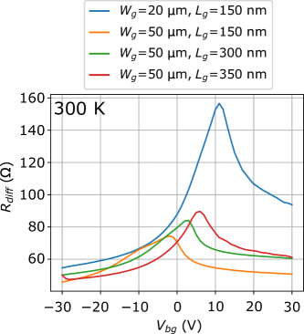
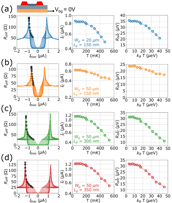
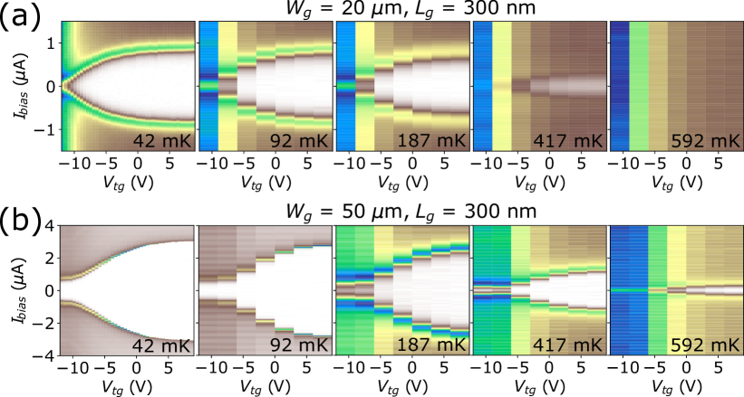
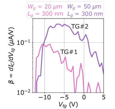
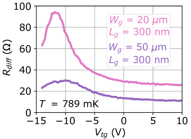
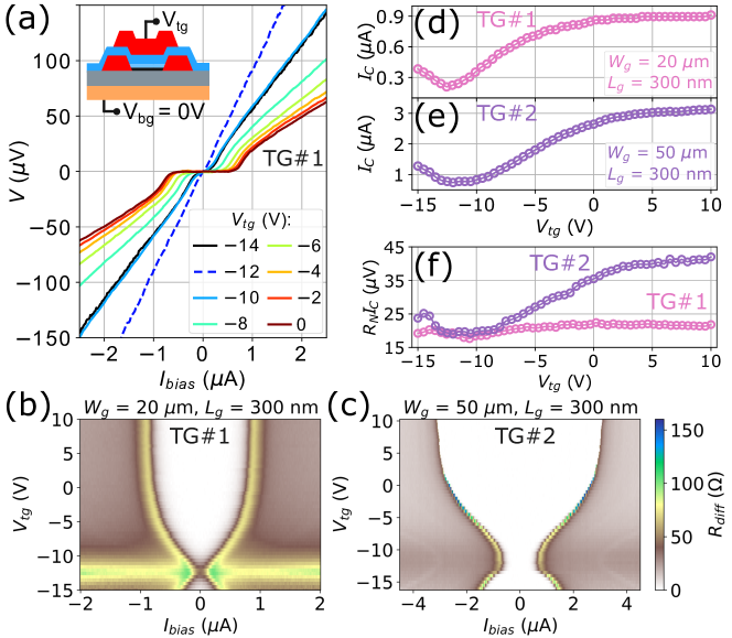
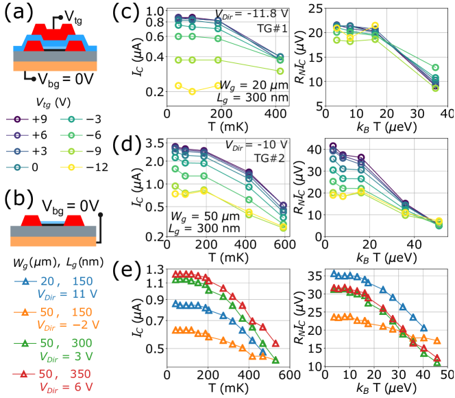
Results and discussion. The optical and scanning-electron-microscope (SEM) images of the final top-gated JoFET, similar to those measured in this paper, are shown in Fig. 1 (a,b). A schematic cross-section of the JoFET is given in Fig. 1(c). Fig. 2 shows the normal-state differential resistance vs top-gate voltage characteristics with an onoff ratio of 3–4 for two JoFETs with gate length nm and width of and 50 , respectively.
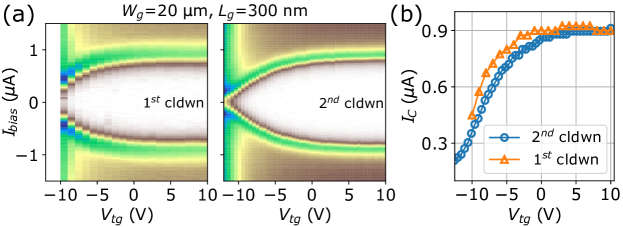
All measurements of the top-gated JJs are done by sweeping from negative to positive voltages to avoid gate-hysteresis effects (see Supplementary Materials). We do not observe current hysteresis, suggesting that our JoFETs are in the over-damped regime. The devices are stable against thermal cycling in terms of and between different cooldowns (see Supplementary Materials).
Following the work by Li et al., 2 on graphene JJs and supported by the results in Refs. 22, 25, 26, we extract the contact resistance , Dirac peak position , and charge carrier concentration (using the model from ref. 27) from the data presented in Fig. 2. As summarized in Table 1 the resulting V ( V), normalized contact resistance ( ) for TG (TG) with (50 ). At V We obtain the mean free path –27 nm from , where is the channel resistance (the total normal-state resistance is ), is the elementary charge, is the Fermi wave vector calculated as , and is the Plank constant.
The superconducting coherence length nm is obtained from , where is the reduced Plank constant, = 90 eV is induced superconducting gap extracted from multiple Andreev reflection (see Supplementary Materials), and is the diffusion coefficient calculated as , with m/s being the Fermi velocity in graphene far from 26. Next, we deduce the Thouless energy –100 eV for the diffusive regime as as , and estimate the JJ transparency –0.09 from 28, where is the number of conducting channels (200 per m of ), defined as . The parameters in Table 1 were extracted far from the Dirac point at V and .
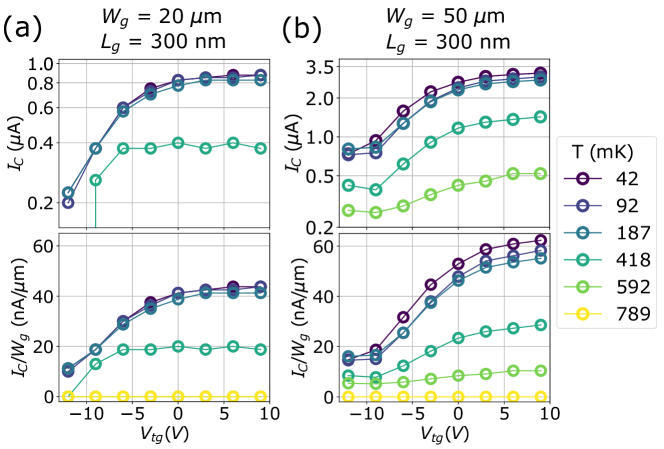
The current–voltage characteristics of the top-gated device with nm and m are shown in Fig. 3(a) for different at 42 mK. The lock-in measurements of as a function of and for devices TG from Fig. 2 are shown in Fig. 3 (b,c). At the same time of acquiring differential resistance 2D maps, we were measuring the gate current leakage, and found that it was below 1 nA (setup limit) for the entire range between 10 V and 15 V. The critical current extracted from Fig. 3(b,c) as a function of is shown in Fig. 3(d,e). The values extracted for positive and negative were symmetric. While for TG, the coherent transport is almost entirely suppressed at , the wider device, TG, has a superconducting plateau which does not close due to the channel inhomogeneity, similar to what has been reported in 4, 7. Despite the difference close to in suppression of supercurrent, for fixed , the ratio at V, 3 /0.9 = 3.3, approximately matches the ratio 50 /25 = 2.5. For the third device, TG with nm and , at V and , we find (see Supplementary material), confirming a good scaling of with geometrical parameters of JJs.
The product of the normal-state resistance and the critical current as a function of is shown in Fig. 3(f). While TG has almost constant as is changed from +10 to 15 V, due to the channel inhomogeneity, the product for TG changes between 20 (close to ) to 40 (far from ). The reduced ratio of (at the short-to-intermediate junction regime with and ) of 0.2–0.4 may be explained by the partial transmission at the graphene/superconductor interface 23.
In the long-junction limit, scales as exp() with 29, and in the short-junction limit, a plateau in is expected 29, 6, 1, 9. For the top-gated devices, and dependencies are shown in Fig. 4 (c-d) as function of . The short-junction behaviour for TG with varying very little between 42 mK and 200 mK, with the rapid decrease of at mK can be observed. While for the ballistic junction we expect to have little variation in the behavior as a function of 6, here we observe that the reduction with is much weaker for closer to for TG.
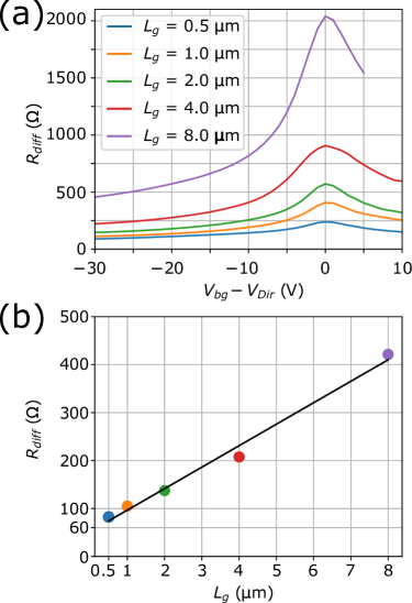
Furthermore, we characterize four un-gated JJs with between 20 and 50 and between 150 nm and 350 nm, see Fig. 4(b). Due to the low-temperature freeze-out of weakly-doped Si substrate acting as a back-gate, we measure the un-gated JJs at as shown in Fig. 4(e), where is deduced from the 300-K measurements (see Supplementary Materials). Qualitatively similar behavior for the un-gated JJs is observed as for TG, suggesting that the top-gate oxide and metal fabrication steps do not significantly affect the JJ properties. As the JJ is biased close to (see the device with , nm, V), and depend weakly on temperature, similar to the top-gated devices. Similar values between 20–40 are observed at for the back-gated JJs as compared to TG.
Finally, we evaluate the transconductance parameter defined as for TG as used in superconducting digital electronics 16, 11 (see the data in Supplementary Materials). Despite a relatively low junction transparency and not optimal gate oxide thickness, we achieve peak values of 0.09 and 0.22 /V for TG and TG, showing a promising linear scaling with .
Conclusion and Outlook. In summary, we have demonstrated 150-mm-wafer scalable fabrication of JoFETs with low contact resistance using CVD graphene and the local top gate control. We observe field-effect-tunable critical current up to a few , shown to have reasonable scaling with gate length and channel width. Our JoFETs operate in the short diffusive regime as measured for seven devices at low temperatures. Operated in the over-damped regime, our devices have a good stability against thermal cycling.
Our JoFETs are fabricated similarly to conventional CMOS-compatible CVD-graphene FETs and our 300K-wafer-scale device yield exceeds 90. As the next milestone, we aim to reduce the down to 50 nm, optimize the position of , and improve the junction transparency toward the wafer-scale realization of graphene quantum integrated circuits such as superconducting quantum interference devices, RF switches and multiplexers. Our process allows to combine normal-state and superconducting FETs on the same chip to explore the hybrid electronics at the circuit and system design level 30, 31, 32, 16, with energy-efficiency improved by the ambipolar behavior of graphene normal-state and superconducting FETs. Alternatively, the heterogeneous integration of graphene JoFETs with commercial CMOS can be envisioned, similar to Ref. 33.
Finally, we expect our wafer-scale fabrication process to be applicable to other 2D semiconductor weak links, such as transition-metal dichalcogenide MoS2 34, WTe2 35, and NbSe2 36.
Acknowledgements. We thank Antti Kemppinen and Pranauv Selvasundaram from VTT for useful discussions and help in maintaining the cryogenic setup. We also thank Bernardo Realista Ferreira for his assistance in cleanroom fabrication.
We acknowledge funding from the Academy of Finland Centre of Excellence program (project nos. 352925, 336810, 336817, and 336819), Union’s Horizon 2020 research and innovation programme under Grant Agreement No. 824109 European Microkelvin Platform (EMP), EU Horizon 2020 Qu-Pilot project no. 101113983, European Research Council under Advanced Grant no. 101053801 (ConceptQ), Horizon Europe programme HORIZON-CL4-2022-QUANTUM-01-SGA via the project 101113946 (OpenSuperQPlus100), HORIZON-RIA Programme under Grant No. 101135240 (JOGATE), the Future Makers Program of the Jane and Aatos Erkko Foundation and the Technology Industries of Finland Centennial Foundation, Business Finland under the Quantum Technologies Industrial (QuTI) project (decision no. 41419/31/2020). H.B. is funded by the Research Council of Finland through the postdoctoral fellowship project CRYOPROC (no. 350325). A.A.G. acknowledges the financial support of the Academy of Finland project no. 343842. This work used VTT’s and OtaNano Micronova cleanroom and measurement laboratory facilities.
References
- Lee et al. 2015 Lee, G.; Kim, S.; Jhi, S.; Lee, H. Ultimately short ballistic vertical graphene Josephson junctions. Nature Communications 2015, 6, 6181
- Li et al. 2016 Li, C.; Guéron, S.; Chepelianskii, A.; Bouchiat, H. Full range of proximity effect probed with superconductor/graphene/superconductor junctions. Physical Review B 2016, 94, 115405
- Lee and Lee 2018 Lee, G. H.; Lee, H. J. Proximity coupling in superconductor-graphene heterostructures. Reports on Progress in Physics 2018, 81
- Heersche et al. 2007 Heersche, H. B.; Jarillo-Herrero, P.; Oostinga, J. B.; Vandersypen, L. M. K.; Morpurgo, A. F. Bipolar supercurrent in graphene. Nature 2007, 446, 56–59
- Ben Shalom et al. 2016 Ben Shalom, M.; Zhu, M. J.; Fal’ko, V. I.; Mishchenko, A.; Kretinin, A. V.; Novoselov, K. S.; Woods, C. R.; Watanabe, K.; Taniguchi, T.; Geim, A. K.; Prance, J. R. Quantum oscillations of the critical current and high-field superconducting proximity in ballistic graphene. Nature Physics 2016, 12, 318–322
- Borzenets et al. 2016 Borzenets, I. V.; Amet, F.; Ke, C. T.; Draelos, A. W.; Wei, M. T.; Seredinski, A.; Watanabe, K.; Taniguchi, T.; Bomze, Y.; Yamamoto, M.; Tarucha, S.; Finkelstein, G. Ballistic Graphene Josephson Junctions from the Short to the Long Junction Regimes. Physical Review Letters 2016, 117, 237002
- Butseraen et al. 2022 Butseraen, G.; Ranadive, A.; Aparicio, N.; Rafsanjani Amin, K.; Juyal, A.; Esposito, M.; Watanabe, K.; Taniguchi, T.; Roch, N.; Lefloch, F.; Renard, J. A gate-tunable graphene Josephson parametric amplifier. Nature Nanotechnology 2022, 17, 1153–1158
- Barati et al. 2021 Barati, F.; Thompson, J. P.; Dartiailh, M. C.; Sardashti, K.; Mayer, W.; Yuan, J.; Wickramasinghe, K.; Watanabe, K.; Taniguchi, T.; Churchill, H.; Shabani, J. Tuning Supercurrent in Josephson Field-Effect Transistors Using h-BN Dielectric. Nano Letters 2021, 21, 1915–1920
- Aggarwal et al. 2021 Aggarwal, K.; Hofmann, A.; Jirovec, D.; Prieto, I.; Sammak, A.; Botifoll, M.; Martí-Sánchez, S.; Veldhorst, M.; Arbiol, J.; Scappucci, G.; Danon, J.; Katsaros, G. Enhancement of proximity-induced superconductivity in a planar Ge hole gas. Physical Review Research 2021, 3, L022005
- Vigneau et al. 2019 Vigneau, F.; Mizokuchi, R.; Zanuz, D. C.; Huang, X.; Tan, S.; Maurand, R.; Frolov, S.; Sammak, A.; Scappucci, G.; Lefloch, F.; De Franceschi, S. Germanium Quantum-Well Josephson Field-Effect Transistors and Interferometers. Nano Letters 2019, 19, 1023–1027
- Wen et al. 2021 Wen, F.; Yuan, J.; Wickramasinghe, K. S.; Mayer, W.; Shabani, J.; Tutuc, E. Epitaxial Al-InAs Heterostructures as Platform for Josephson Junction Field-Effect Transistor Logic Devices. IEEE Transactions on Electron Devices 2021, 68, 1524–1529
- Xiang et al. 2006 Xiang, J.; Vidan, A.; Tinkham, M.; Westervelt, R. M.; Lieber, C. M. Ge/Si nanowire mesoscopic Josephson junctions. Nature Nanotechnology 2006, 1, 208–213
- Calado et al. 2015 Calado, V. E.; Goswami, S.; Nanda, G.; Diez, M.; Akhmerov, A. R.; Watanabe, K.; Taniguchi, T.; Klapwijk, T. M.; Vandersypen, L. M. K. Ballistic Josephson junctions in edge-contacted graphene. Nature Nanotechnology 2015, 10, 761–764
- Casparis et al. 2018 Casparis, L.; Connolly, M. R.; Kjaergaard, M.; Pearson, N. J.; Kringhøj, A.; Larsen, T. W.; Kuemmeth, F.; Wang, T.; Thomas, C.; Gronin, S.; Gardner, G. C.; Manfra, M. J.; Marcus, C. M.; Petersson, K. D. Superconducting gatemon qubit based on a proximitized two-dimensional electron gas. Nature Nanotechnology 2018, 13, 915–919
- Phan et al. 2023 Phan, D.; Falthansl-Scheinecker, P.; Mishra, U.; Strickland, W.; Langone, D.; Shabani, J.; Higginbotham, A. Gate-Tunable Superconductor-Semiconductor Parametric Amplifier. Physical Review Applied 2023, 19, 1
- Wen et al. 2019 Wen, F.; Shabani, J.; Tutuc, E. Josephson Junction Field-Effect Transistors for Boolean Logic Cryogenic Applications. IEEE Transactions on Electron Devices 2019, 66, 5367–5374
- Kokkoniemi et al. 2020 Kokkoniemi, R.; Girard, J. P.; Hazra, D.; Laitinen, A.; Govenius, J.; Lake, R. E.; Sallinen, I.; Vesterinen, V.; Partanen, M.; Tan, J. Y.; Chan, K. W.; Tan, K. Y.; Hakonen, P.; Möttönen, M. Bolometer operating at the threshold for circuit quantum electrodynamics. Nature 2020, 586, 47–51
- Sardashti et al. 2020 Sardashti, K.; Dartiailh, M. C.; Yuan, J.; Hart, S.; Gumann, P.; Shabani, J. Voltage-Tunable Superconducting Resonators: A Platform for Random Access Quantum Memory. IEEE Transactions on Quantum Engineering 2020, 1, 1–7
- Li et al. 2019 Li, T.; Gallop, J. C.; Hao, L.; Romans, E. J. Scalable, Tunable Josephson Junctions and DC SQUIDs Based on CVD Graphene. IEEE Transactions on Applied Superconductivity 2019, 29, 1–4
- Schmidt et al. 2023 Schmidt, P.; Banszerus, L.; Frohn, B.; Blien, S.; Watanabe, K.; Taniguchi, T.; Hüttel, A. K.; Beschoten, B.; Hassler, F.; Stampfer, C. Tuning the supercurrent distribution in parallel ballistic graphene Josephson junctions. Physical Review Applied 2023, 20, 054049
- Bonmann et al. 2019 Bonmann, M.; Asad, M.; Yang, X.; Generalov, A.; Vorobiev, A.; Banszerus, L.; Stampfer, C.; Otto, M.; Neumaier, D.; Stake, J. Graphene Field-Effect Transistors With High Extrinsic and . IEEE Electron Device Letters 2019, 40, 131–134
- Xia et al. 2011 Xia, F.; Perebeinos, V.; Lin, Y.-m.; Wu, Y.; Avouris, P. The origins and limits of metal–graphene junction resistance. Nature Nanotechnology 2011, 6, 179–184
- Ke et al. 2016 Ke, C. T.; Borzenets, I. V.; Draelos, A. W.; Amet, F.; Bomze, Y.; Jones, G.; Craciun, M.; Russo, S.; Yamamoto, M.; Tarucha, S.; Finkelstein, G. Critical Current Scaling in Long Diffusive Graphene-Based Josephson Junctions. Nano Letters 2016, 16, 4788–4791
- Ludwig et al. 2023 Ludwig, F.; Generalov, A.; Holstein, J.; Murros, A.; Viisanen, K.; Prunnila, M.; Roskos, H. G. Photothermoelectric and resistive self-mixing response contributions in graphene field-effect transistor THz detectors. 2023, arXiv:2311.12382
- Cayssol et al. 2009 Cayssol, J.; Huard, B.; Goldhaber-Gordon, D. Contact resistance and shot noise in graphene transistors. Physical Review B 2009, 79, 075428
- Castro Neto et al. 2009 Castro Neto, A. H.; Guinea, F.; Peres, N. M. R.; Novoselov, K. S.; Geim, A. K. The electronic properties of graphene. Reviews of Modern Physics 2009, 81, 109–162
- Kim et al. 2009 Kim, S.; Nah, J.; Jo, I.; Shahrjerdi, D.; Colombo, L.; Yao, Z.; Tutuc, E.; Banerjee, S. Realization of a high mobility dual-gated graphene field-effect transistor with Al2O3 dielectric. Applied Physics Letters 2009, 94, 062107
- Datta 1995 Datta, S. Electronic Transport in Mesoscopic Systems; Cambridge University Press, Cambridge, 1995
- Tinkham 1996 Tinkham, M. Introduction to Superconductivity; McGraw-Hill, New York, 1996
- Van Duzer and Kumar 1990 Van Duzer, T.; Kumar, S. Semiconductor-superconductor hybrid electronics. Cryogenics 1990, 30, 1014–1023
- Zhao et al. 2017 Zhao, Q.-Y.; McCaughan, A. N.; Dane, A. E.; Berggren, K. K.; Ortlepp, T. A nanocryotron comparator can connect single-flux-quantum circuits to conventional electronics. Superconductor Science and Technology 2017, 30, 044002
- Alam et al. 2020 Alam, S.; Jahangir, M. A.; Aziz, A. A Compact Model for Superconductor- Insulator-Superconductor (SIS) Josephson Junctions. IEEE Electron Device Letters 2020, 41, 1249–1252
- Soikkeli et al. 2023 Soikkeli, M.; Murros, A.; Rantala, A.; Txoperena, O.; Kilpi, O.-P.; Kainlauri, M.; Sovanto, K.; Maestre, A.; Centeno, A.; Tukkiniemi, K.; Gomes Martins, D.; Zurutuza, A.; Arpiainen, S.; Prunnila, M. Wafer-Scale Graphene Field-Effect Transistor Biosensor Arrays with Monolithic CMOS Readout. ACS Applied Electronic Materials 2023, 5, 4925–4932
- Trainer et al. 2020 Trainer, D. J.; Wang, B.; Bobba, F.; Samuelson, N.; Xi, X.; Zasadzinski, J.; Nieminen, J.; Bansil, A.; Iavarone, M. Proximity-Induced Superconductivity in Monolayer MoS2. ACS Nano 2020, 14, 2718–2728
- Randle et al. 2023 Randle, M. D.; Hosoda, M.; Deacon, R. S.; Ohtomo, M.; Zellekens, P.; Watanabe, K.; Taniguchi, T.; Okazaki, S.; Sasagawa, T.; Kawaguchi, K.; Sato, S.; Ishibashi, K. Gate-Defined Josephson Weak-Links in Monolayer WTe2. Advanced Materials 2023, 35, 2301683
- Bauriedl et al. 2022 Bauriedl, L.; Bäuml, C.; Fuchs, L.; Baumgartner, C.; Paulik, N.; Bauer, J. M.; Lin, K.-Q.; Lupton, J. M.; Taniguchi, T.; Watanabe, K.; Strunk, C.; Paradiso, N. Supercurrent diode effect and magnetochiral anisotropy in few-layer NbSe2. Nature Communications 2022, 13, 4266
Supplementary materials: Wafer-scale CMOS-compatible graphene Josephson field-effect transistors
In the Supplementary materials document, we give a more detailed description of the fabrication process in section S1: Fabrication, further details of the room temperature 4-probe DC I-V probe-station characterization in section S2: Room temperature characterization. In section S3: Additional low-temperature data, we show the supporting cryogenic data for the graphene JoFET devices from the main text, and data from an additional top-gated device TG.
S1: Fabrication
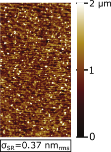
The graphene JoFETs are fabricated on a 150 mm (6") p-type Si substrate with a 90 nm SiO2 oxide layer to enable the substrate back gate measurements at room temperature. The CVD graphene is transferred by Graphenea™ on the full wafer. The main feature of the fabrication process is the encapsulation of the CVD graphene with a thin layer of Al2O3, deposited by evaporation of Al, oxidized in the evaporation chamber. This Al2O3 layer of oxide protects graphene from wet lithography processes and residues of resist. Next, the e-beam lithography (EBL) for superconducting contacts is done on top of graphene and Al2O3 encapsulation layer, and the Al2O3 in the contact area is etched. The etching of Al2O3 encapsulation layer is done before the superconducting Al contacts evaporation and it is the most important step for the yield of JoFETs. The incomplete etch of the oxide results in a Schottky barrier at the contact interface and weakens the superconducting proximity coupling between the Al Source/Drain and graphene. The quality of etching is controlled by Atomic Force Microscopy (AFM) operated in the capacitive mode on the surface of cleaned and etched graphene, before the contacts evaporation (see Supplementary Fig. 1). There, we obtain the surface roughness as low as 370 pm. After that, the contacts are evaporated with Ti/Al stack followed by a lift-off process. As the final step, the gate dielectric Al2O3 is grown using the atomic layer deposition (ALD), and the gate electrode is patterned with EBL on top of gate dielectric, evaporated with Ti/Al stack, and followed by a lift-off process.
S2: Room temperature characterization
At room temperature, the graphene FETs are characterized with a semiconductor parameter analyzer using an automated probe station on wafer level. The DC transfer curves (drain-source resistance vs top- and/or back-gate voltage) of all the JoFETs are measured to estimate the yield of fabrication, which for this fabrication run was found to be 90. The probed device arrays include JoFETs with varying gate length and channel width . The data normalized to the Dirac peak position are shown in Supplementary Fig. 3(a). Furthermore, the contact resistance is extracted by the Transfer Length Method (TLM), using the liner fit on the data with different . The TLM fitting for data in Supplementary Fig. 3(a) is shown in Supplementary Fig. 3(b) (the total normal-state differential resistance is shown). The contact resistance for the device with nm is 60 , and approximating to zero, it results in normalized to the channel width for the probed devices of 300 , which is comparable to the low-temperature measured for TG at sub-K temperature from the main text. The estimation of the contact resistance is done on relatively long FETs with from 0.5 to 8 to avoid short channel effects.
Superconducting top-gated and un-gated junctions studied in the main text were in the range of from 150 to 350 . The room temperature ) data for the un-gated junctions discussed in the main text in Fig. 4 (e) are shown in Supplementary Fig. 2 (see also Supplementary Fig. 4). One can notice a wider spread in the Dirac peak position for the un-gated devices as compared to the top-gated devices TG (see Fig. 2 in the main text and Supplementary Fig. 11).
S3: Cryogenic characterization
The additional data for the un-gated devices presented in Fig. 4(e) from the main text, are shown in Supplementary Fig.4, where each un-gated junction is plotted and analyzed individually. There, the black open circle markers in the left panels of (a-d) show the extraction procedure, using which, we track the local maximums of to extract (here only shown for the negative as we obtained the same results for the positive extraction). The middle and right panels duplicate the data from Fig. 4(e) of the main text where four devices’ and values as a function of temperature were plotted in the same plots.
The 2D maps of as function of and at different temperatures from 42 mK to 592 mK, used to extract and data presented in the main text in Fig. 4(c,d), are given in Supplementary Fig. 5. The maps measured for TG were obtained by sweeping from negative to positive values (see the discussion on gate-hysteresis and Supplementary Fig. 7 below).
Different way of representing the dependencies as a function of temperature is plotted in Supplementary Fig. 6 (see the upper panels of (a,b)). The critical current normalized by the geometrical width is given in the lower panels of (a,b), showing a good, almost linear scaling with .
The graphene FET and JJ devices are prone to experience strong dependence of the parameters such as and between different cooldowns. In Supplementary Fig. 7, we provide the data from the device TG (analyzed in the main text) for two different cooldowns. Note that while the Dirac point seem to be almost identical, since in the 1st cooldown, the device was measured starting from V, there is a slight discrepancy in the dependence. This is due to the gate-hysteresis effect discussed further below. Overall, a good reproducibility between several different cooldowns was observed for the top-gated Josephson junctions.
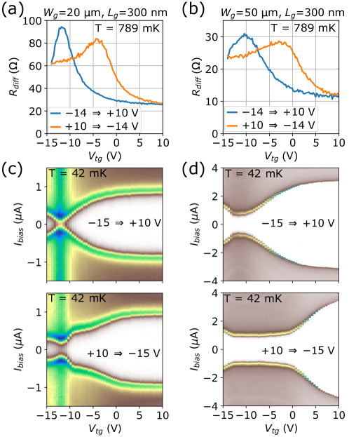
In Supplementary Fig. 8, the gate-hysteresis effect of TG is studied in the normal-state operation shown in (a-b) and using the 2D maps recorded for the same devices below the critical temperature as shown in (c-d). While the exact origin of gate hysteresis is beyond the scope of this paper, we assume that it originates from the traps at the graphene/ALD oxide and in the gate oxide. In this sense, using a different ALD gate oxide, such as HfO could be beneficial to reduce the gate hysteresis. For both, the normal-state and superconducting plateau characteristics, we observe reproducible gate-hysteresis between several consecutive and non-consecutive up-down and down-up sweeps.
The transconductance parameter for TG is given in Supplementary Fig. 9. We note that similarly to the conventional FETs, one straightforward way to boost it (as relevant for the digital superconducting electronics applications, where the output of one JoFET is expected to trigger another JoFET) is to reduce the gate-oxide thickness or use a high-k dielectric such as HfO.
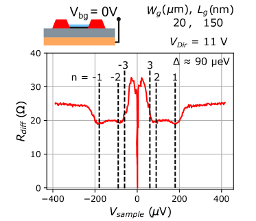
The Multiple Andreev reflection (MAR) features obtained in the DC-voltage-biased 4 probe configuration, a common method to extract the induced superconducting gap in superconducting proximity junctions, are presented in Supplementary Fig. 10. While we only measured MAR in the voltage biased configurations for 1 un-gated device, assuming the Bardeen–Cooper–Schrieffer (BCS) theory applies and the superconducting gap is , the critical temperature, , estimated based on = 90 of 600 mK is compatible with the data for both un-gated and top-gated devices shown in Fig. 4 of the main text.
Finally, the additional data for the 3rd top-gated device measured at 300 K and 42 mK are shown in Supplementary Fig. 11(a) and (c). Due to the shorted top- and back-gate wire-bonds, at base temperature, only data at V were measured. Similarly to all the other devices, we did not see any significant current hysteresis as illustrated in panel (b) of Supplementary Fig. 11.