Atomic Layer Molecular Beam Epitaxy of Kagome Magnet RMn6Sn6 (R = Er, Tb) Thin Films
Abstract
Kagome lattices have garnered substantial interest because their band structure consists of topological flat bands and Dirac cones. The RMn6Sn6 (R = rare earth) compounds are particularly interesting because of the existence of large intrinsic anomalous Hall effect (AHE) which originates from the gapped Dirac cones near the Fermi level. This makes RMn6Sn6 an outstanding candidate for realizing the high-temperature quantum anomalous Hall effect. The growth of RMn6Sn6 thin films is beneficial for both fundamental research and potential applications. However, most of the studies on RMn6Sn6 have focused on bulk crystals so far, and the synthesis of RMn6Sn6 thin films has not been reported so far. Here we report the atomic layer molecular beam epitaxy growth, structural and magnetic characterizations, and transport properties of ErMn6Sn6 and TbMn6Sn6 thin films. It is especially noteworthy that TbMn6Sn6 thin films have out-of-plane magnetic anisotropy, which is important for realizing the quantum anomalous Hall effect. Our work paves the avenue toward the control of the AHE using devices patterned from RMn6Sn6 thin films.
Materials with layered kagome structures provide an ideal platform for studying the interplay between band structure and magnetism. In momentum space, a two-dimensional kagome lattice manifests Dirac cones at the K points Kuroda et al. (2017); Ye et al. (2018), saddle points at the M points Kang et al. (2022); Teng et al. (2023), and a flat band across the Brillouin zone Kang et al. (2020a, b). The introduction of magnetism and spin-orbital coupling further opens a gap at the band touching points, leading to topologically nontrivial electronic states Sun et al. (2011); Guo and Franz (2009); Bolens and Nagaosa (2019). In real space, non-trivial spin textures (e.g. magnetic skyrmions) have been observed in kagome magnets Hou et al. (2017); Li et al. (2023).
Recently, RMn6Sn6 (R = rare earth) compounds have emerged as a new family of topological kagome magnets Yin et al. (2020); Ma et al. (2021). The Mn atoms in RMn6Sn6 form Mn3 kagome layers and the spin ordering of the Mn3 layers is largely affected by the R atoms. Previous studies on bulk crystals report that R = Gd, Tb, Dy, and Ho give rise to ferromagnetic coupling of Mn spins, while R = Er, Tm, and Lu lead to antiferromagnetic coupling of Mn spins at zero field Venturini, El Idrissi, and Malaman (1991); Malaman et al. (1999); Clatterbuck and Gschneidner Jr (1999). Rare earth elements in RMn6Sn6 compounds also provide one additional knob for tuning the magnetocrystalline anisotropy (MCA) which is connected to the Dirac gap opening Cheng et al. (2023). Large Berry-curvature-induced intrinsic anomalous Hall effect (AHE) may originate from the gapped Dirac cones close to the Fermi level, because the intrinsic anomalous Hall conductivity (AHC) is connected to the Dirac gap opening and the Dirac cone position through Sinitsyn et al. (2007):
| (1) |
Notably, TbMn6Sn6 bulk crystals exhibit out-of-plane magnetic anisotropy, which leads to a 34 meV Dirac gap opening at 130 meV above the Fermi level Yin et al. (2020), and band structure calculations predict the quantum anomalous Hall effect (QAHE) if the Fermi level could be tuned into the gap. Experimentally, the observation of a giant intrinsic AHC of =0.14 e2/ per kagome layer in TbMn6Sn6 bulk crystals Yin et al. (2020) makes the RMn6Sn6 family of materials attractive for QAHE. To this end, the growth of RMn6Sn6 thin films provides opportunities for tuning the band structure and Fermi level through epitaxial strain, chemical doping, or voltage gating. However, all of the reported works have focused on bulk crystals of RMn6Sn6, while studies on their thin film counterparts have been missing. Therefore, the development of epitaxial RMn6Sn6 thin films is highly desired.
In this paper, we report the growth of (0001)-oriented thin films of ErMn6Sn6 and TbMn6Sn6 using atomic layer molecular beam epitaxy (AL-MBE) and characterize their magnetic and transport properties. The films are grown on Pt(111) buffer layers on Al2O3(0001) substrates. Various methods are employed to characterize the structure of our samples, including in-situ reflection high energy electron diffraction (RHEED), X-ray diffraction (XRD), and atomic force microscopy (AFM). We demonstrate that the magnetic properties of RMn6Sn6 thin films can be tuned through the selection of rare earth element . ErMn6Sn6 thin films favor in-plane (IP) magnetization, while TbMn6Sn6 thin films undergo an out-of-plane (OOP) to IP spin-reorientation transition (SRT) as the temperature increases above 300 K. Lastly, we find that the longitudinal resistance of RMn6Sn6/Pt bilayers do not follow a simple parallel resistor model but instead depends on the electron mean free path and can be explained qualitatively by the Fuchs-Sondheimer model.
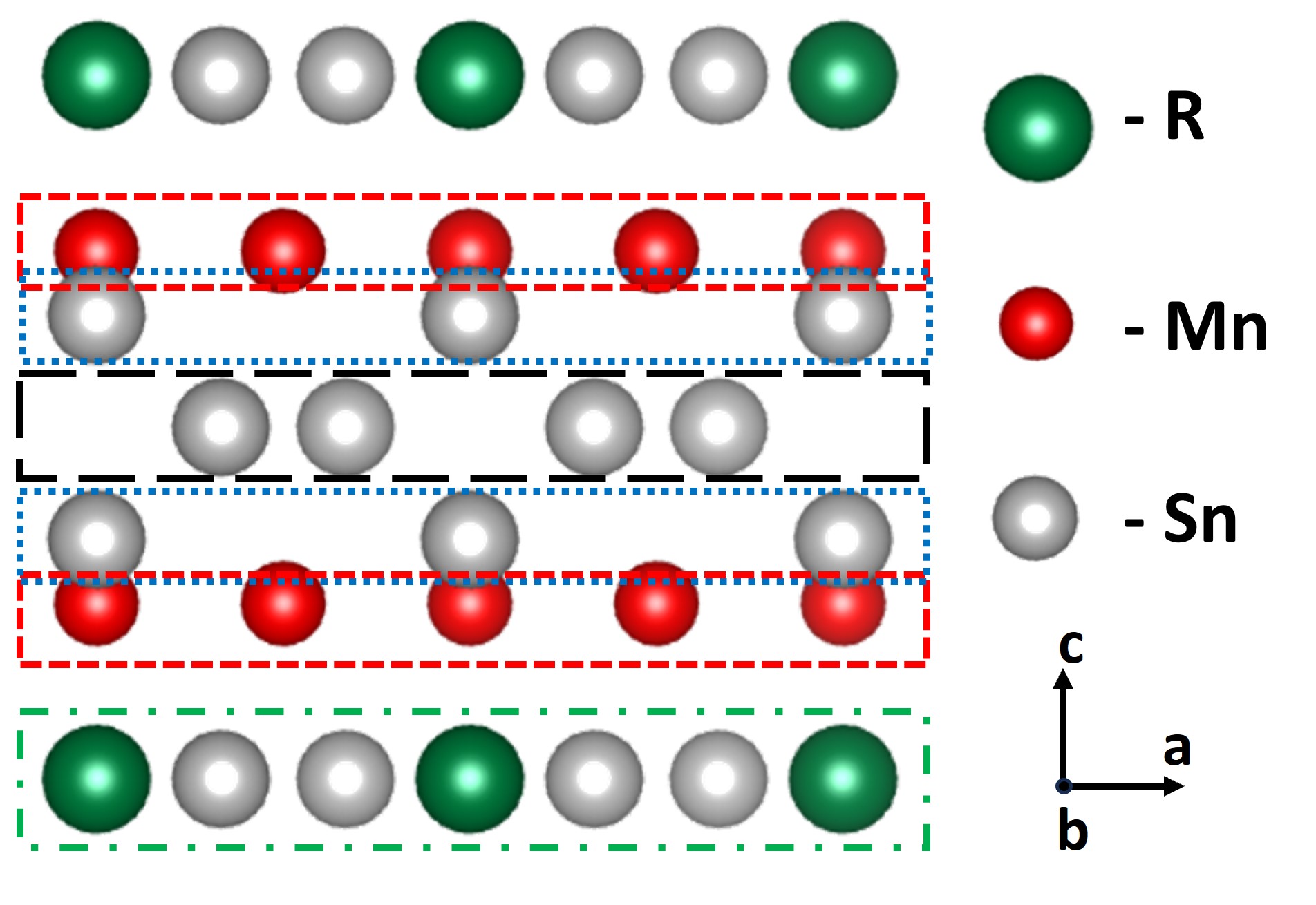
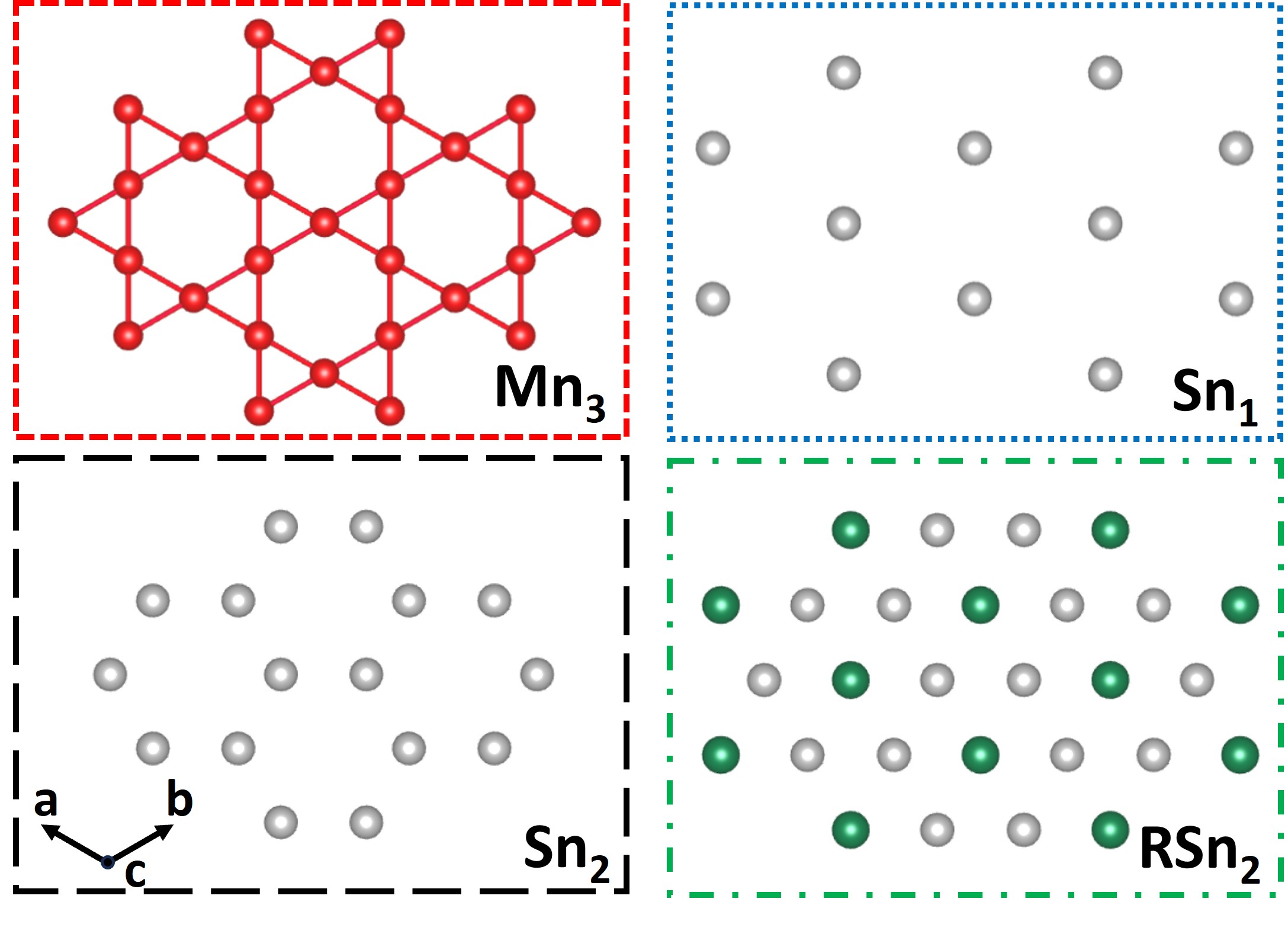
The crystal structure of RMn6Sn6 is displayed in Fig. 1, featuring a hexagonal lattice (space group , lattice constants a = 5.5 Å and c = 9.0 Å) with atomic layers stacked along the c-axis Malaman, Venturini, and Roques (1988). In each unit cell, there are two kagome Mn3 layers closely neighboured by two Sn1 layers, with one honeycomb Sn2 layer inserted between two Sn1 layers, and one RSn2 layer inserted between Mn3 kagome layers. Inspired by this stacking sequence, we develop an AL-MBE recipe to grow ErMn6Sn6 and TbMn6Sn6 thin films on epitaxial Pt(111) buffer layers on Al2O3(0001) substrates. In AL-MBE, atomic layers are grown sequentially by opening and closing the appropriate MBE source shutters with precise timing. A similar growth strategy allowed us to synthesize thin films of another kagome magnet, Fe3Sn2, which also has a hexagonal layered lattice structure Cheng et al. (2022).
The base pressure of the growth chamber is 110-9 Torr. The Al2O3(0001) substrates (MTI corporation) are annealed in air at 1000 ∘C for 3 hours, then degassed in-situ at 500 ∘C for 30 minutes to prepare a flat and clean surface. A 5 nm epitaxial Pt(111) buffer layer is subsequently grown on Al2O3(0001) following the recipe described in our previous work Cheng et al. (2022). The ErMn6Sn6(0001) and TbMn6Sn6(0001) thin films are grown on Pt(111) buffer layers at 100 ∘C and 80 ∘C, respectively using the AL-MBE recipe described below. First, the kagome Mn3 layer and hexagonal Sn1 layer are co-deposited with flux ratio Mn:Sn = 3:1, then the honeycomb RSn2 is deposited with flux ratio Er:Sn (or Tb:Sn) = 2:1, then another hexagonal Sn1 layer and kagome Mn3 layer are co-deposited, then one Sn2 layer is deposited. The aforementioned shutter growth sequence is repeated until the desired thickness (typically 20 nm) of RMn6Sn6 is achieved. Typical deposition rates are 1.6 Å/min, 1.6 Å/min, 3.9 Å/min, and 2.8 Å/min for Er, Tb, Mn, and Sn, respectively. After growth, a 5 nm CaF2 layer is deposited to prevent sample oxidation.
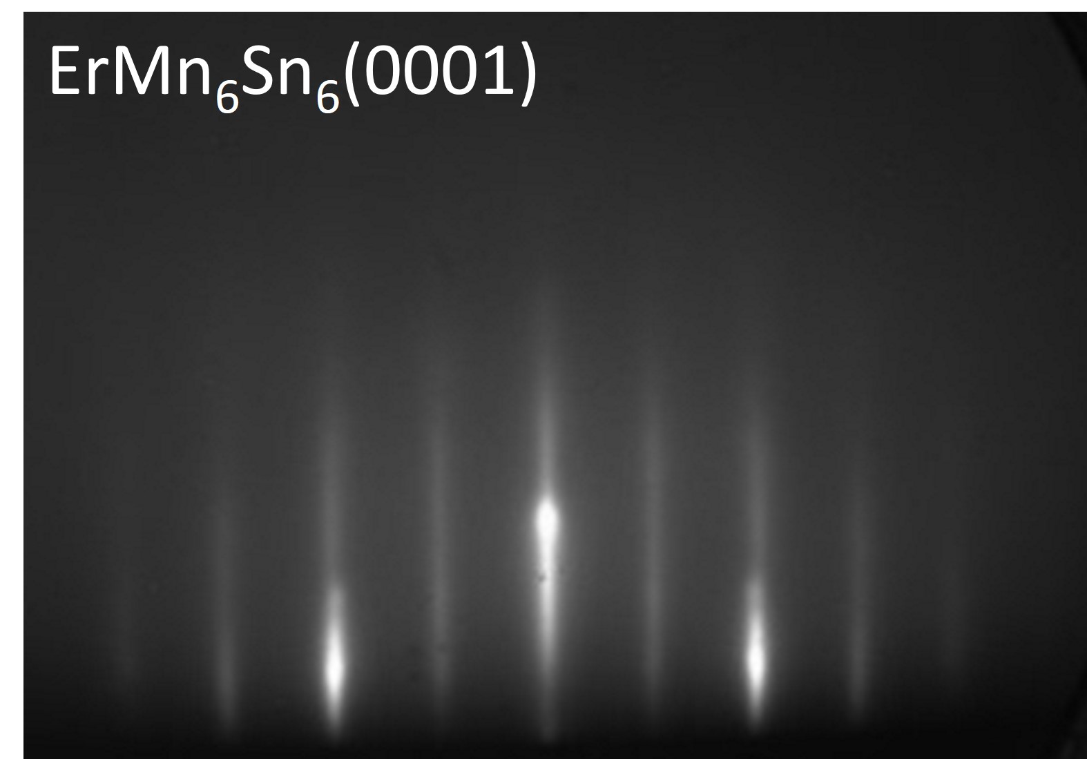
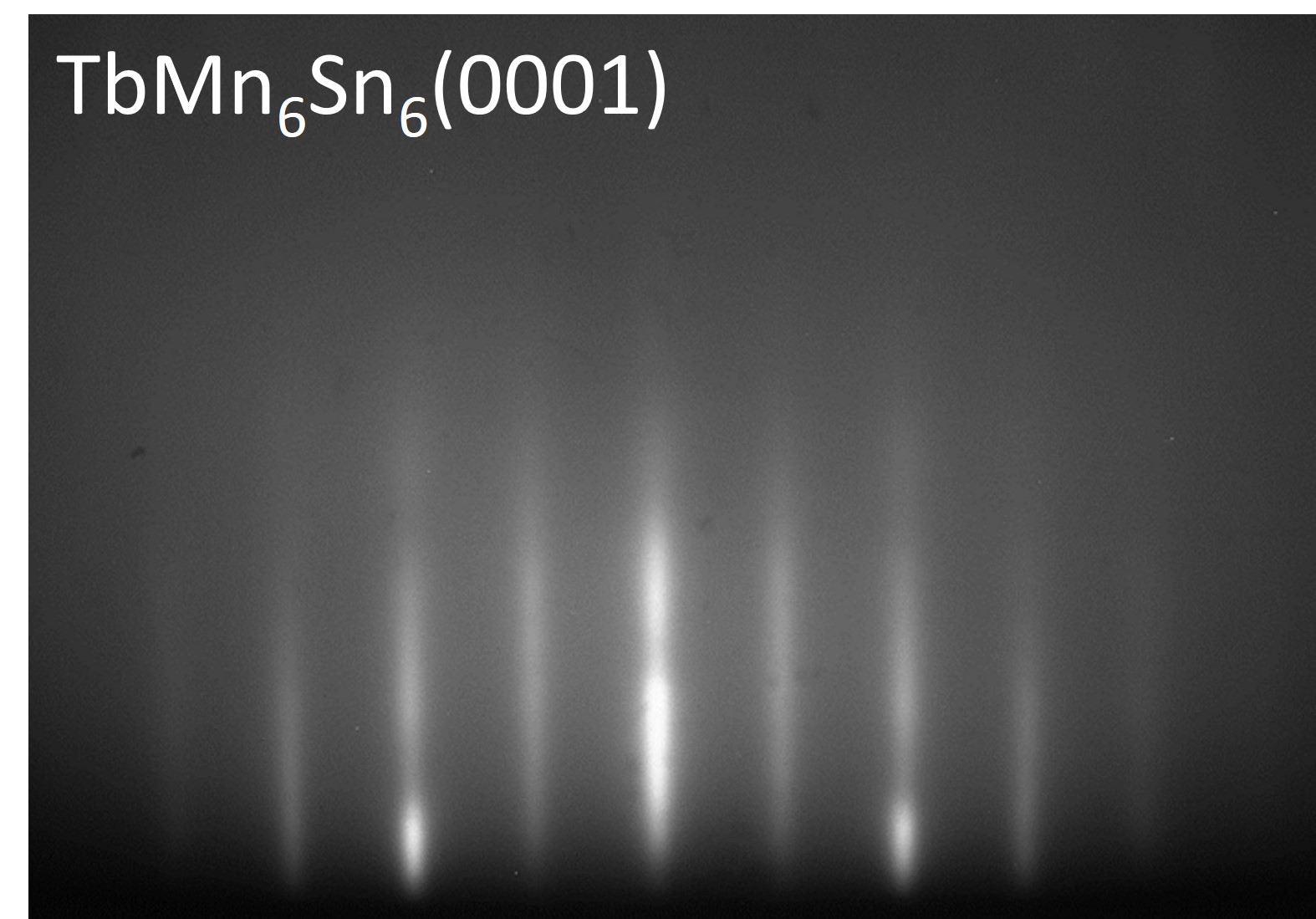
The in-situ RHEED patterns of ErMn6Sn6 and TbMn6Sn6 are monitored during the growths. The RHEED patterns of a 20 nm ErMn6Sn6 thin film and a 20 nm TbMn6Sn6 thin film along Al2O3[110] direction are shown in Fig. 1c and 1d, respectively. The RHEED patterns are generally streaky, suggesting the morphology of our RMn6Sn6 thin films is dominated by two-dimensional terraces with finite sizes, although some three-dimensional features also exist as spots. The RHEED pattern suggests the in-plane lattice constants for our samples are = 5.47 Å, and = 5.56 Å, respectively, and the in-plane epitaxial relationship is RMn6Sn6[100]Pt[110]Al2O3[110].
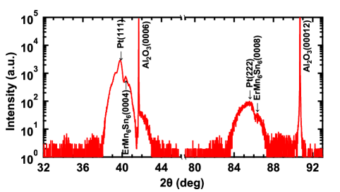
We perform XRD measurements to confirm the crystallographic structures of ErMn6Sn6 and TbMn6Sn6 thin films. The X-ray is from the Cu-K radiation, with a wavelength of 1.5406 Å. Fig. 2a shows the XRD data of a 20 nm ErMn6Sn6 thin film. Next to the substrate peaks at 41.57∘ and 90.60∘, two major peaks are found at 39.78∘ and 85.46∘, respectively. These peaks are attributed to Pt(111) and Pt(222) peaks because their 2 angles convert to out-of-plane lattice constants of 2.275 Å and 2.270 Å, respectively. These values are close to the out-of-plane lattice constant of Pt along (111) direction (3.923 Å= 2.265 Å) Rooksby and Lewis (1964). ErMn6Sn6(0004) and ErMn6Sn6(0008) peaks appear as nearby shoulder peaks at 40.36∘ and 87.63∘, respectively. The out-of-plane lattice constant of ErMn6Sn6 extracted from (0004) peak is 8.93 Å, which is close to but slightly smaller than the reported bulk value of 9.0006 Å Clatterbuck, Lange, and Gschneidner Jr (1999).
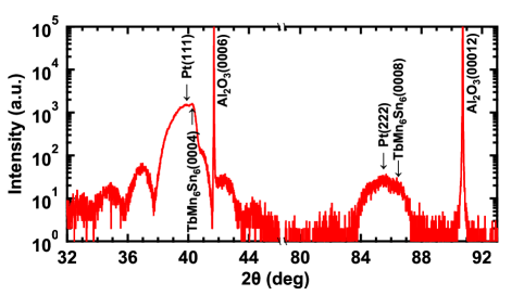
For TbMn6Sn6 thin film, the general characteristics of the XRD data are similar to ErMn6Sn6. To the right of Pt(111) peak which is at 39.88∘, the TbMn6Sn6(0004) peak is found as a shoulder peak (see Fig. 2c). A double Gaussian peak fitting yields TbMn6Sn6(0004) peak position of 40.26∘, which corresponds to an out-of-plane lattice of c = 8.95 Å. This is also smaller than the reported bulk value of 9.0208 Å Clatterbuck, Lange, and Gschneidner Jr (1999).
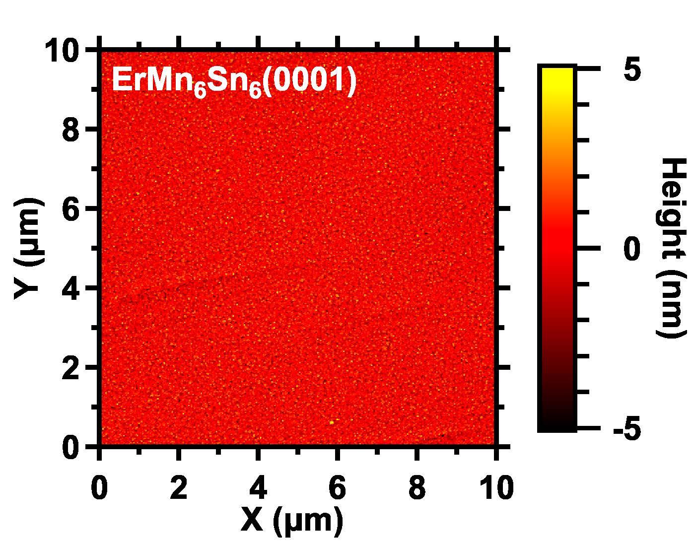
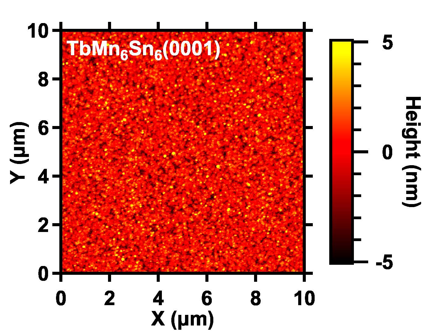
We characterize the surface morphology of ErMn6Sn6 and TbMn6Sn6 thin films using AFM. Fig. 2b shows the AFM image of a 20 nm ErMn6Sn6 sample grown at 100∘C. The film has a continuous and flat surface with sub-micron grain size. The root-mean-square (rms) roughness of the 20 nm ErMn6Sn6 sample is 1.02 nm. Fig. 2b shows the AFM image of a 20 nm TbMn6Sn6 sample grown at 80∘C. The rms roughness of the 20 nm TbMn6Sn6 sample is 1.45 nm.
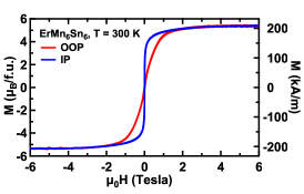
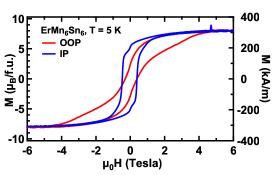
To investigate the magnetic properties of the RMn6Sn6 thin films, we perform SQUID magnetometer measurements. Fig. 3a shows the IP (blue) and OOP (red) hysteresis loops of a 20 nm ErMn6Sn6 thin film. The IP hysteresis loop has a smaller saturation field of 0.2 Tesla, while the OOP hysteresis loop has a larger saturation field of 1.7 Tesla, indicating ErMn6Sn6 has easy-plane anisotropy at room temperature. The saturation magnetization of ErMn6Sn6 thin film is 5.4 /f.u. (212 kA/m) at room temperature. The IP and OOP hysteresis loops of ErMn6Sn6 at T = 5 K are shown in Fig. 3b. At T = 5 K, both IP and OOP hysteresis loops show much larger coercive fields and larger saturation fields, while the saturation field of the OOP hysteresis loop is still larger than the IP hysteresis loop. The IP loop exhibits a sharper switching behavior, with the coercive field of 0.47 Tesla. Meanwhile, the OOP hysteresis loop becomes narrower near zero field and wider at higher fields. The coercive field of the OOP hysteresis loop is 0.30 Tesla.
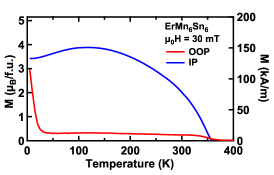
We also measure the temperature-dependence of remanence magnetization of the ErMn6Sn6 thin film, as shown in Fig. 3c. For both OOP (the red curve) and IP (the blue curve) measurements, the sample is cooled down under 7 Tesla applied field, and measured at low field while heating up. A 30 mT field is applied to set the polarity of the magnetization. From the temperature-dependent magnetization curve, the Curie temperature of the 20 nm ErMn6Sn6 thin film is determined to be 353 K, signified by a drop of magnetization to zero. This Curie temperature is consistent with the reported value of 350 K on ErMn6Sn6 bulk crystals Clatterbuck and Gschneidner Jr (1999).
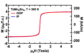
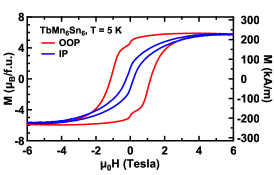
Compared to ErMn6Sn6 thin films, TbMn6Sn6 thin films show different magnetic properties. Fig. 3d and 3e show the hysteresis loops of a 25 nm TbMn6Sn6 thin film at 300 K and 5 K, respectively. At T = 300 K, the OOP (red) and IP (blue) hysteresis loops of TbMn6Sn6 are almost identical, with a saturation field of 0.6 Tesla (see Fig. 3d). The saturation magnetization of TbMn6Sn6 is 3.9 /f.u. (154 kA/m) at room temperature. While cooling down to T = 5 K, the OOP hysteresis loop of TbMn6Sn6 exhibits a square shape, with tails extended to 5 Tesla, as shown in Fig. 3e Meanwhile, the IP hysteresis loop shows a gradual switching behavior. At zero field, the OOP remanence magnetization is much larger than the IP remanence magnetization, suggesting that TbMn6Sn6 favors OOP at T = 5 K.
The perpendicular magnetic anisotropy is highly unusual for epitaxial kagome magnet thin films, as most of the previously reported kagome magnet thin films have easy-plane anisotropy Taylor et al. (2020); Hong et al. (2020); Khadka et al. (2020); Cheng et al. (2021, 2022); Fujiwara et al. (2023). Even for epitaxial Fe3Sn2 whose bulk form has MCA along the c-axis, the MCA is overcome by the magnetic shape anisotropy (MSA) which favors easy-plane anisotropy. As a result, both MBE-grown and sputtered Fe3Sn2 thin films manifest easy-plane anisotropy Khadka et al. (2020); Cheng et al. (2022). However, in TbMn6Sn6 thin films, the MCA is strong enough to overcome the MSA and leads to an easy-axis anisotropy at low temperatures. It is noteworthy that such large magnetocrystalline anisotropy along the c-axis opens a gap at the Dirac cone, leading to a large intrinsic AHE Yin et al. (2020); Ma et al. (2021).
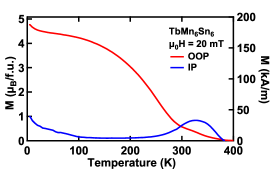
The perpendicular magnetic anisotropy of the TbMn6Sn6 thin film sample at low temperatures is further confirmed by the temperature-dependent SQUID measurements, as shown in Fig. 3f. A 20 mT field is applied to set the polarity of the magnetization. Below 300 K, the OOP magnetization (red curve) is always larger than the IP magnetization (blue curve). A crossover between IP and OOP magnetization happens at T = 300 K above which the IP magnetization becomes larger than the OOP magnetization. This crossover suggests an OOP-to-IP SRT as the temperature increases above 300 K. A similar temperature-induced SRT has been observed at 310 K in TbMn6Sn6 bulk crystals Clatterbuck and Gschneidner Jr (1999) and is reported to be related to the formation of magnetic skyrmions Li et al. (2023). Both IP and OOP magnetization eventually disappears above the Curie temperature which is determined to be 380 K. This Curie temperature is lower than the reported value of 423 K on TbMn6Sn6 bulk crystals Venturini, El Idrissi, and Malaman (1991).
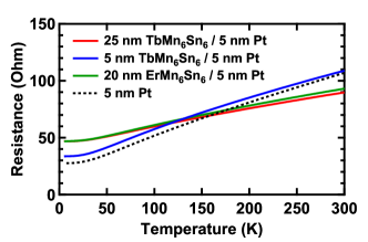
We next discuss the transport properties of ErMn6Sn6/Pt and TbMn6Sn6/Pt thin films. The transport measurements are performed using Quantum Design Physical Property Measurement System (PPMS) on 300 m100 m Hall bar devices patterned from ErMn6Sn6/Pt and TbMn6Sn6/Pt thin films. The longitudinal resistance of the Hall bar devices at zero field is shown in Fig. 4a. Comparing between TbMn6Sn6(25 nm)/Pt(5 nm) bilayer (the red curve) and Pt(5 nm) single layer (the black dashed curve), the bilayer resistance is lower than the Pt single layer resistance for higher temperatures (T200 K). This is consistent with the parallel resistor model in which the TbMn6Sn6 and Pt layers are modeled as two resistors connected in parallel and therefore have smaller resistance than the Pt layer alone. The parallel resistor model has been widely used to extract the resistivity of kagome material thin films grown on metallic buffer layers Hong et al. (2020); Khadka et al. (2020); Cheng et al. (2021); Thapaliya et al. (2021). However, at low temperatures (T150 K), the resistance of the TbMn6Sn6(25 nm)/Pt(5 nm) bilayer is larger than that of the Pt(5 nm) single layer. This is the opposite of what one would expect from the parallel resistor model. The comparison between ErMn6Sn6(20 nm)/Pt(5 nm) bilayer (the green curve) and Pt(5 nm) single layer shows a similar trend that the bilayer resistance is smaller than the Pt single layer resistance for T200 K and larger than the Pt single layer resistance for T100 K. The deviation from the parallel resistor model is more pronounced for the bilayers with smaller kagome layer thicknesses. For example, for TbMn6Sn6(5 nm)/Pt(5 nm) bilayer (the blue curve), the resistance is larger than Pt(5 nm) single layer from T=5 K up to T=300 K.
The deviation from the parallel resistor model can be explained by Fuchs-Sondheimer theory, in which the resistance of bilayers depends not only on the bulk resistance of two materials but also the mean free path of electrons in them Fuchs (1938); Sondheimer (1952). In the Fuchs-Sondheimer model, when the electron mean free path is much smaller than the thickness of each layer, the bilayer resistance is smaller than the resistance of individual layers. In this case, the Fuchs-Sondheimer model converges to the parallel resistor model. However, when the electron mean free path is much larger than the thickness of each layer, the bilayer resistance is larger than the resistance of individual layers, which is more similar to the series resistor model. Especially in an infinite superlattice consisting of alternating stacking of two materials with the same thickness, in the thin layer limit and under the assumption that the electron densities in two materials are identical, the averaged resistivity of the superlattice is exactly equal to the average value of the bulk resistivity of the two materials Misra et al. (1999). In our RMn6Sn6/Pt bilayer samples, the scattering length is shorter than the individual layer thickness at high temperatures, therefore the bilayer resistance is smaller than the resistance of Pt layer, similar to the parallel resistor model. Meanwhile, at low temperatures or with smaller thicknesses, the mean free path becomes longer than the individual layer thickness, and the bilayer resistance is larger than the resistance of Pt layer, similar to the series resistor model. Due to the complexity of data analysis, extracting the intrinsic longitudinal resistivity of ErMn6Sn6 and TbMn6Sn6 from bilayer resistance is outside the scope of this paper.
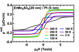
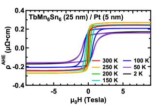
We also measured the anomalous Hall effect (AHE) of ErMn6Sn6(20 nm)/Pt(5 nm) and TbMn6Sn6(25 nm)/Pt(5 nm) bilayers, as shown in Fig. 4b and Fig. 4c, respectively. Here, the anomalous Hall resistivity is calculated by multiplying the anomalous Hall resistance by the thickness of the RMn6Sn6 layer. For ErMn6Sn6, the AHE hysteresis loop at K has a large remanence, a low-field opening (with the coercive field of T) and a large saturation field ( T). The opening of the hysteresis loop decreases quickly as the temperature increases, and almost disappears before the temperature reaches 100 K. For TbMn6Sn6, the AHE hysteresis loops are relatively square, with the coercive field decreasing as temperature increases. For both materials, as temperature increases from 2 K to 300 K, the amplitude of AHE first increases, reaches the maximum value between 200 K and 250 K, and then decreases. This behavior is understood as follows. The anomalous Hall resistivity scales with where is between and . The intrinsic and side-jump contributions yield and skew-scattering yields . Tian, Ye, and Jin (2009) Since increases with temperature (Figure 4a), this scaling explains the enhancement of with temperature as observed below 200 K. On the other hand, the reduction of AHE resistivity at higher temperatures can be attributed to the decrease in magnetization as the temperature approaches the Curie temperature.
In conclusion, this study demonstrates the synthesis of -plane ErMn6Sn6 and TbMn6Sn6 thin films using atomic layer molecular beam epitaxy. A combination of RHEED, XRD, and AFM confirms the structure of the samples. Magnetization measurements show that ErMn6Sn6 has easy-plane anisotropy from 5 K to room temperature, while TbMn6Sn6 has perpendicular magnetic anisotropy at low temperature and an OOP-to-IP spin reorientation as the temperature increases above 300 K. Transport measurements at low temperatures show that the longitudinal resistance of the RMn6Sn6/Pt bilayer is larger than that of the Pt layer alone, which is inconsistent with the parallel resistance model. On the other hand, such behavior is qualitatively explained by the Fuchs-Sondheimer model. Lastly, since both ErMn6Sn6 and TbMn6Sn6 are synthesized under similar conditions, other members of the RMn6Sn6 family could likely be grown using similar AL-MBE recipes. These results create a solid foundation for future research and applications based on RMn6Sn6 thin films.
Acknowledgments
We acknowledge Daniel Halbing, Katherine Robinson, and Xueshi Gao for their assistance in the construction of the evaporation cells. S.C. was supported by NSF Grant No. CHE-1935885. I.L. was supported by the Center for Emergent Materials, an NSF MRSEC, under Grant No. DMR-2011876. W.Z. was supported by AFOSR MURI 2D MAGIC Grant No. FA9550-19-1-0390 and the US Department of Energy Grant No. DE-SC0016379.
Author Declarations
Conflict of Interest
The authors declare no conflicts of interest to disclose.
Data Availability Statement
The data that support the findings of this study are available from the corresponding author upon reasonable request.
References
References
- Kuroda et al. (2017) K. Kuroda, T. Tomita, M.-T. Suzuki, C. Bareille, A. Nugroho, P. Goswami, M. Ochi, M. Ikhlas, M. Nakayama, S. Akebi, R. Noguchi, R. Ishii, N. Inami, K. Ono, H. Kumigashira, A. Varykhalov, T. Muro, T. Koretsune, R. Arita, S. Shin, T. Kondo, and S. Nakatsuji, “Evidence for magnetic Weyl fermions in a correlated metal,” Nature materials 16, 1090–1095 (2017).
- Ye et al. (2018) L. Ye, M. Kang, J. Liu, F. Von Cube, C. R. Wicker, T. Suzuki, C. Jozwiak, A. Bostwick, E. Rotenberg, D. C. Bell, L. Fu, R. Comin, and J. G. Checkelsky, “Massive Dirac fermions in a ferromagnetic kagome metal,” Nature 555, 638–642 (2018).
- Kang et al. (2022) M. Kang, S. Fang, J.-K. Kim, B. R. Ortiz, S. H. Ryu, J. Kim, J. Yoo, G. Sangiovanni, D. Di Sante, B.-G. Park, C. Jozwiak, A. Bostwick, E. Rotenberg, E. Kaxiras, S. D. Wilson, J.-H. Park, and R. Comin, “Twofold van Hove singularity and origin of charge order in topological kagome superconductor CsV3Sb5,” Nature Physics 18, 301–308 (2022).
- Teng et al. (2023) X. Teng, J. S. Oh, H. Tan, L. Chen, J. Huang, B. Gao, J.-X. Yin, J.-H. Chu, M. Hashimoto, D. Lu, C. Jozwiak, A. Bostwick, E. Rotenberg, G. E. Granroth, B. Yan, R. J. Birgeneau, P. Dai, and M. Yi, “Magnetism and charge density wave order in kagome FeGe,” Nature Physics , 1–9 (2023).
- Kang et al. (2020a) M. Kang, S. Fang, L. Ye, H. C. Po, J. Denlinger, C. Jozwiak, A. Bostwick, E. Rotenberg, E. Kaxiras, J. G. Checkelsky, and R. Comin, “Topological flat bands in frustrated kagome lattice CoSn,” Nature communications 11, 4004 (2020a).
- Kang et al. (2020b) M. Kang, L. Ye, S. Fang, J.-S. You, A. Levitan, M. Han, J. I. Facio, C. Jozwiak, A. Bostwick, E. Rotenberg, M. K. Chan, R. D. McDonald, D. Graf, K. Kaznatcheev, E. Vescovo, D. C. Bell, E. Kaxiras, J. van den Brink, M. Richter, M. P. Ghimire, C. J. G., and R. Comin, “Dirac fermions and flat bands in the ideal kagome metal FeSn,” Nature materials 19, 163–169 (2020b).
- Sun et al. (2011) K. Sun, Z. Gu, H. Katsura, and S. D. Sarma, “Nearly flatbands with nontrivial topology,” Physical Review Letters 106, 236803 (2011).
- Guo and Franz (2009) H.-M. Guo and M. Franz, “Topological insulator on the kagome lattice,” Physical Review B 80, 113102 (2009).
- Bolens and Nagaosa (2019) A. Bolens and N. Nagaosa, “Topological states on the breathing kagome lattice,” Physical Review B 99, 165141 (2019).
- Hou et al. (2017) Z. Hou, W. Ren, B. Ding, G. Xu, Y. Wang, B. Yang, Q. Zhang, Y. Zhang, E. Liu, F. Xu, W. Wang, G. Wu, X. Zhang, B. Shen, and Z. Zhang, “Observation of various and spontaneous magnetic skyrmionic bubbles at room temperature in a frustrated kagome magnet with uniaxial magnetic anisotropy,” Advanced Materials 29, 1701144 (2017).
- Li et al. (2023) Z. Li, Q. Yin, Y. Jiang, Z. Zhu, Y. Gao, S. Wang, J. Shen, T. Zhao, J. Cai, H. Lei, S.-Z. Lin, Y. Zhang, and B. Shen, “Discovery of topological magnetic textures near room temperature in quantum magnet TbMn6Sn6,” Advanced Materials , 2211164 (2023).
- Yin et al. (2020) J.-X. Yin, W. Ma, T. A. Cochran, X. Xu, S. S. Zhang, H.-J. Tien, N. Shumiya, G. Cheng, K. Jiang, B. Lian, Z. Song, G. Chang, I. Belopolski, D. Multer, M. Litskevich, Z.-J. Cheng, X. P. Yang, B. Swidler, H. Zhou, H. Lin, T. Neupert, Z. Wang, N. Yao, T.-R. Chang, S. Jia, and M. Z. Hasan, “Quantum-limit Chern topological magnetism in TbMn6Sn6,” Nature 583, 533–536 (2020).
- Ma et al. (2021) W. Ma, X. Xu, J.-X. Yin, H. Yang, H. Zhou, Z.-J. Cheng, Y. Huang, Z. Qu, F. Wang, M. Z. Hasan, and S. Jia, “Rare earth engineering in RMn6Sn6 (R = Gd - Tm, Lu) topological kagome magnets,” Physical review letters 126, 246602 (2021).
- Venturini, El Idrissi, and Malaman (1991) G. Venturini, B. C. El Idrissi, and B. Malaman, “Magnetic properties of RMn6Sn6 (R= Sc, Y, Gd–Tm, Lu) compounds with HfFe6Ge6 type structure,” Journal of magnetism and magnetic materials 94, 35–42 (1991).
- Malaman et al. (1999) B. Malaman, G. Venturini, R. Welter, J. Sanchez, P. Vulliet, and E. Ressouche, “Magnetic properties of RMn6Sn6 (R= Gd–Er) compounds from neutron diffraction and Mössbauer measurements,” Journal of magnetism and magnetic materials 202, 519–534 (1999).
- Clatterbuck and Gschneidner Jr (1999) D. Clatterbuck and K. Gschneidner Jr, “Magnetic properties of RMn6Sn6 (R= Tb, Ho, Er, Tm, Lu) single crystals,” Journal of magnetism and magnetic materials 207, 78–94 (1999).
- Cheng et al. (2023) Z.-J. Cheng, I. Belopolski, H.-J. Tien, T. A. Cochran, X. P. Yang, W. Ma, J.-X. Yin, D. Chen, J. Zhang, C. Jozwiak, et al., “Visualization of tunable Weyl line in A–A stacking kagome magnets,” Advanced Materials 35, 2205927 (2023).
- Sinitsyn et al. (2007) N. Sinitsyn, A. MacDonald, T. Jungwirth, V. Dugaev, and J. Sinova, “Anomalous Hall effect in a two-dimensional Dirac band: The link between the Kubo-Streda formula and the semiclassical Boltzmann equation approach,” Physical Review B 75, 045315 (2007).
- Malaman, Venturini, and Roques (1988) B. Malaman, G. Venturini, and B. Roques, “New ternary stannides: MMn6Sn6 (M = Sc, Y, Sm, Gd-Tm, Lu) AND ScFe6Sn6,” Materials research bulletin 23, 1629–1633 (1988).
- Cheng et al. (2022) S. Cheng, B. Wang, I. Lyalin, N. Bagués, A. J. Bishop, D. W. McComb, and R. K. Kawakami, “Atomic layer epitaxy of kagome magnet Fe3Sn2 and Sn-modulated heterostructures,” APL Materials 10, 061112 (2022).
- Rooksby and Lewis (1964) H. Rooksby and B. Lewis, “Relations between the structures of phases in the system platinum-molybdenum,” Journal of the Less Common Metals 6, 451–460 (1964).
- Clatterbuck, Lange, and Gschneidner Jr (1999) D. Clatterbuck, R. Lange, and K. Gschneidner Jr, “Magneto-optical properties of RMn6Sn6 (R= Gd, Tb, Dy, Ho, Er, Tm, Lu) single crystals,” Journal of magnetism and magnetic materials 195, 639–645 (1999).
- Taylor et al. (2020) J. M. Taylor, A. Markou, E. Lesne, P. K. Sivakumar, C. Luo, F. Radu, P. Werner, C. Felser, and S. S. Parkin, “Anomalous and topological Hall effects in epitaxial thin films of the noncollinear antiferromagnet Mn3Sn,” Physical Review B 101, 094404 (2020).
- Hong et al. (2020) D. Hong, N. Anand, C. Liu, H. Liu, I. Arslan, J. E. Pearson, A. Bhattacharya, and J. Jiang, “Large anomalous nernst and inverse spin-hall effects in epitaxial thin films of kagome semimetal Mn3Ge,” Physical Review Materials 4, 094201 (2020).
- Khadka et al. (2020) D. Khadka, T. Thapaliya, S. H. Parra, J. Wen, R. Need, J. M. Kikkawa, and S. Huang, “Anomalous Hall and Nernst effects in epitaxial films of topological kagome magnet Fe3Sn2,” Physical review materials 4, 084203 (2020).
- Cheng et al. (2021) Y. Cheng, S. Yu, M. Zhu, J. Hwang, and F. Yang, “Tunable topological Hall effects in noncollinear antiferromagnet Mn3Sn/Pt bilayers,” APL Materials 9, 051121 (2021).
- Fujiwara et al. (2023) K. Fujiwara, Y. Kato, H. Abe, S. Noguchi, J. Shiogai, Y. Niwa, H. Kumigashira, Y. Motome, and A. Tsukazaki, “Berry curvature contributions of kagome-lattice fragments in amorphous Fe–Sn thin films,” Nature Communications 14, 3399 (2023).
- Thapaliya et al. (2021) T. Thapaliya, T. Yoo, S. Hurtado Parra, N. D. Arndt, R. Need, J. M. Kikkawa, H. Kim, and S. Huang, “High-quality epitaxial thin films of topological kagome metal CoSn by magnetron sputtering,” Applied Physics Letters 119, 201902 (2021).
- Fuchs (1938) K. Fuchs, “The conductivity of thin metallic films according to the electron theory of metals,” in Mathematical Proceedings of the Cambridge Philosophical Society, Vol. 34 (Cambridge University Press, 1938) pp. 100–108.
- Sondheimer (1952) E. Sondheimer, “The mean free path of electrons in metals,” Advances in Physics 1, 1–42 (1952).
- Misra et al. (1999) A. Misra, M. Hundley, D. Hristova, H. Kung, T. Mitchell, M. Nastasi, and J. Embury, “Electrical resistivity of sputtered Cu/Cr multilayered thin films,” Journal of Applied Physics 85, 302–309 (1999).
- Tian, Ye, and Jin (2009) Y. Tian, L. Ye, and X. Jin, “Proper scaling of the anomalous Hall effect,” Physical review letters 103, 087206 (2009).