otherfnsymbols ††‡‡§§¶¶
Distance dependence of the energy transfer mechanism in WS2 - graphene heterostructures
Abstract
We report on the mechanism of energy transfer in van der Waals heterostructures of the two-dimensional semiconductor WS2 and graphene with varying interlayer distances, achieved through spacer layers of hexagonal boron nitride (hBN). We record photoluminescence and reflection spectra at interlayer distances between 0.5 nm and 5.8 nm (0-16 hBN layers). We find that the energy transfer is dominated by states outside the light cone, indicative of a Förster transfer process, with an additional contribution from a Dexter process at 0.5 nm interlayer distance. We find that the measured dependence of the luminescence intensity on interlayer distances above 1 nm can be quantitatively described using recently reported values of the Förster transfer rates of thermalized charge carriers. At smaller interlayer distances, the experimentally observed transfer rates exceed the predictions and furthermore depend on excess energy as well as on excitation density. Since the transfer probability of the Förster mechanism depends on the momentum of electron-hole pairs, we conclude that at these distances, the transfer is driven by non-thermalized charge carrier distributions.
In low-dimensional systems, materials in proximity couple via near-field interactions, which can result in the transfer of energy from one material to the other Förster (1949); Persson and Lang (1982). This interaction is not only central to light-driven processes in biological systems, including photosynthesis in plants Mirkovic et al. (2017), but is also exploited in applications, such as organic light emitting diodes Yang and Neher (2006) or in protein imaging Pollok and Heim (1999). It furthermore appears in many artificial low-dimensional hybrid systems, such as quantum dots Chen et al. (2010), semiconductor nano-platelets Federspiel et al. (2015) or molecular systems on graphene Treossi et al. (2009); Gaudreau et al. (2013), as well as in van der Waals (vdW) heterostructures, e.g. of the transition metal dichalcogenides (TMDs) and graphene He et al. ; Hill et al. (2017); Froehlicher et al. (2018); Aeschlimann et al. (2020). These 2D heterostructures are of particular interest with respect to possible applications, such as flexible electronics Georgiou et al. (2013), photodetectors Britnell et al. (2013); Zhang et al. (2014) or photovoltaics Bernardi et al. (2013); Nassiri Nazif et al. (2021), the performance of which might be diminished or improved by energy transfer between the layers. To take full advantage of the opportunities these heterostructures provide, a microscopic understanding of the mechanisms of the energy transfer is therefore of central importance.
Different mechanisms can contribute to the transfer of energy. The Dexter coupling describes electrons and holes which transfer independently due to an overlap of the respective wave functions. It therefore decreases exponentially with the distance between the materials Dexter (1953). The Förster coupling is a dipole-dipole interaction, which is mediated by virtual photons and can therefore be significant also on larger interlayer distances Persson and Lang (1982); Swathi and Sebastian (2009). Theoretical works predict the Förster coupling to generally dominate in vdW heterostructures consisting of TMDs and graphene Malic et al. (2014); Selig et al. (2019a). Microscopically, these works predict the rates to display a strong dependence on in-plane momentum of the excited electron-hole pairs, which vanishes for Malic et al. (2014); Selig et al. (2019a). This particular momentum-dependence implies that the life time of excitons within the light cone does not depend on the total transfer rate and, accordingly, the transfer to be dominated by excitations at larger momenta.
Experimental studies in vdW heterostructures so far have focused on TMDs in direct contact with graphene. Some have argued that the energy transfer in these heterostructures proceeds via tunneling Krause et al. (2021), whereas others concluded the transfer to be dominated by a Förster interaction Gaudreau et al. (2013); Federspiel et al. (2015). Experiments conducted at large excitation densities were interpreted as being driven by a modified Förster transfer, facilitated by hot holes in graphene Dong et al. (2023). The dependence on interlayer distance has so far not been experimentally tested, and the techniques applied did not allow inferring information on the momentum-dependence of the transfer rates.
The aim of this letter is to experimentally address the microscopic origins of the energy transfer in 2D heterostructures. The distance dependence of the energy transfer rates is measured via the quenching of photoluminescence (PL) of WS2 in the proximity to graphene using spacer layers of hBN of varying thickness Britnell et al. (2012); Brotons-Gisbert et al. (2019); Tebbe et al. (2023a). A dependence of the transfer rates on the momentum is observed in measurements of the line width of the luminescence, which originates from excitons within the light cone, as well as by varying the excitation condition in the PL experiments, which induces different transient electronic momentum distributions in the TMD and results in different levels of PL quenching.
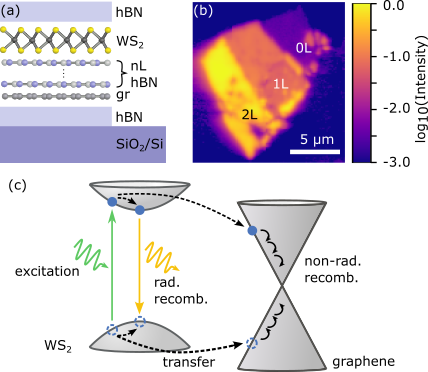
Heterostructures of WS2, hBN spacer layers and graphene were prepared by tape exfoliation of the individual materials, automated detection of suited flakes Uslu et al. (2023), followed by mechanical stacking (see Tebbe et al. (2023a) for details). In total, eight different samples were studied in this work, with spacers ranging from zero to 16 layers of hBN. This corresponds to distances between WS2 and graphene of 0.5 nm to 5.8 nm, assuming a WS2-hBN layer separation of 0.5 nm Rooney et al. (2017) and a graphene-hBN layer separation of 0.33 nm Pease (1950); Haigh et al. (2012). A sketch of the sample structures is shown in Fig. 1 (a).
All samples were characterized by taking high-resolution reflectance contrast as well as photoluminescence maps at room temperature using a hyperspectral imaging setup Tebbe et al. (2023b). An example of the spectrally integrated PL intensity of a sample containing 0, 1 and 2 hBN spacer layers (0L, 1L and 2L), excited with a 532 nm laser, is shown in Fig. 1 (b) (note the logarithmic intensity scale). The three areas can be distinguished in the raw image by the markedly different PL intensities, which differ by about one order of magnitude between adjacent spacer layer thicknesses. The magnitude of the PL quenching is a result of the competition between relaxation and radiative recombination of electron-hole pairs within WS2 and energy transfer to graphene, which is followed by nonradiative recombination. A sketch of the two competing processes is shown in Fig. 1 (c).
We first analyze the absorption and emission line widths in areas of different spacer layers, which are related to the lifetime of excitons within the light cone. Exemplary PL and reflection contrast spectra are shown in Figs. 2 (a) and (b). The PL spectra are well described by a single Lorentzian peak, except for areas without graphene, which show small signatures of additional trion emission Mak et al. (2013). This suggests that the WS2 crystal possesses some level of electron doping, and that these electrons transfer into the graphene Froehlicher et al. (2018) for all spacer layer thicknesses up to 5.8 nm. The shape of the exciton absorption feature in the white light reflection contrast spectra is a result of thin film interference, which depends on the thicknesses of all layers of the sample and the substrate Arora et al. (2015). The redshift observed in both the absorption and emission peaks with proximity to graphene is due to the increasing dielectric screening from the graphene layer Raja et al. (2017); Tebbe et al. (2023a).
Fitting the emission and absorption spectra at all positions of all samples, we obtain distributions for the line width of every spacer layer. From these, we extract the minimum line width and their error (see supplemental material for details SI ). These values are shown as a function of the number of hBN spacer layers in Fig. 2 (c).
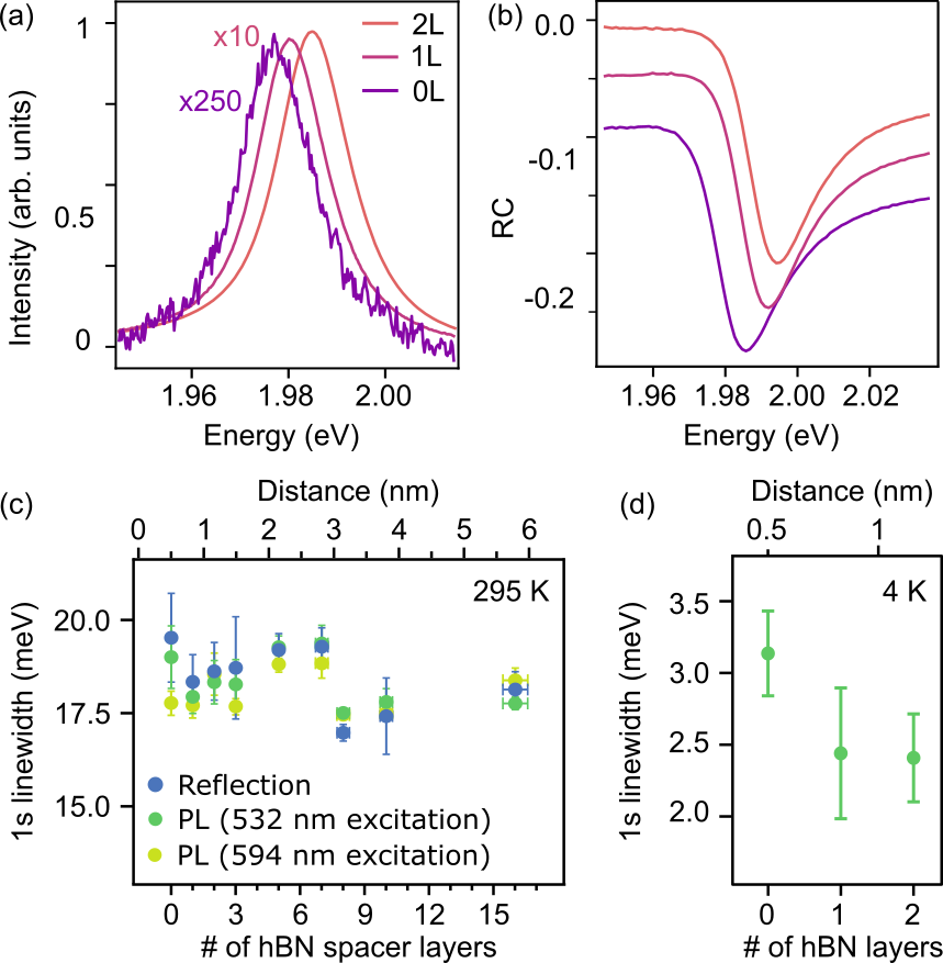
Within the errors of the experiment, absorption and emission line widths are found to be constant across all layer separations, with a possible increase only for the TMD in direct contact with graphene. The observed variations between layer thicknesses likely originate from the different statistical weight of the various samples contributing to each data point. The minimum line width between samples can slightly depend on sample geometry, i.e. the top and bottom hBN thicknesses, due to the Purcell effect Fang et al. (2019).
To verify the broadening at small interlayer distances, we performed additional experiments on a single sample containing 0, 1 and 2 spacer layers at a temperature of 4 K, at which phonon-related broadening is reduced, see Fig. 2 (d). These data yield a broadening of the exciton peak for 0 spacer layers of meV compared to the peaks of 1 and 2 hBN layers, for which no significant difference in the FWHM is found. We note that the broadening observed here is much smaller compared to earlier work, which found an increase of meV when WS2 was placed on graphene Hill et al. (2017), but is similar to data on TMD/graphene heterostructures published more recently Lorchat et al. (2020). As in the former of the studies, samples were prepared on SiO2, the broadening may not be systematic but likely resulted from inhomogeneities of the substrate Raja et al. (2019).
The broadening of the exciton peak allows first conclusions on the mechanism of the energy transfer. As the Förster transfer rates have been shown to approach zero for a momentum transfer of Malic et al. (2014); Selig et al. (2019a), this interaction is not expected to affect excitons within the light-cone. Our data therefore suggests that a Dexter process significantly contributes to the energy transfer at 0.5 nm interlayer distance (0 spacer layers), but not necessarily at larger interlayer distances. As the PL intensity is quenched by several orders of magnitude, while the observed broadening is smaller than the initial line width, we conclude that a different process is responsible for the majority of the energy transfer.
We now evaluate the quenching of the PL emission as a function of the graphene-WS2 distance. To experimentally cover the full range of distances, the PL intensities of different samples have to be compared to each other. Care needs to be taken in such a comparison, as absorption and emission of the sample are subject to thin film interference, which depends on the sample geometry, i.e. the order and thicknesses of the layers within the stack. We do account for this by comparing intensities of areas within the same samples, which differ by the number of spacer layers only. Intensities between samples are normalized by areas of common spacer thickness.
The plot of the relative luminescence intensity vs spacer thickness is shown in Figure 3. The measured PL intensity decreases with proximity to graphene, with the most drastic changes between layer thicknesses observed at interlayer distances smaller than 1 nm. In total, the intensity is reduced by more than three orders of magnitude between WS2 in direct contact with graphene and the largest distance studied (5.8 nm). We also note that the PL intensity in areas without graphene is significantly smaller than the one at 16 spacer layers, which we attribute to the residual doping of these areas (see discussion above).
The measured luminescence intensity depends on the competing processes of radiative recombination and non-radiative transfer to graphene, with the associated rates and , respectively. Here we assume the radiative recombination rate to be independent of the interlayer distance, . Therefore, the PL intensity is connected to the rates by:
| (1) |
where denotes the interlayer distance Gómez-Santos and Stauber (2011). Non-radiative decay within the TMD is also assumed to be unaffected by the presence of graphene; it then does not qualitatively influence the results and will be neglected in the following.
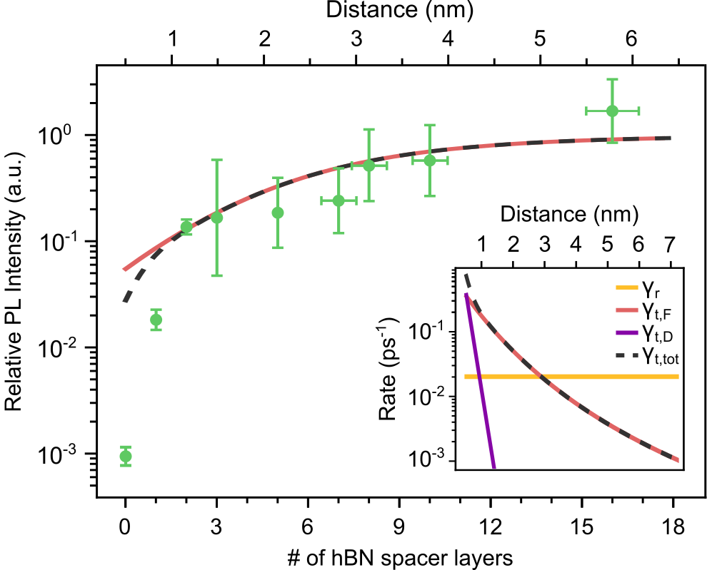
The connection between transfer rates and luminescence intensity allows us to compare our measurements to a recent theory of the distance dependence of the Förster energy transfer between WS2 and graphene Selig et al. (2019a). The transfer probabilities of charge carriers have been shown to depend on interlayer distance and the total momentum of the electron-hole pairs as
| (2) |
Assuming the carriers to be thermalized, i.e. them following a Boltzmann distribution, an effective transfer rate can then be calculated. Since the increased line width at 0 spacer layers demonstrates a contribution from Dexter coupling, which is neglected in the theory, we also add a phenomenological Dexter term, such that .
We calculate the Förster rates using the parameters given in Selig et al. (2019a) with an effective (i.e. frequency-averaged) dielectric constant of hBN of Steinhoff et al. (2018); Waldecker et al. (2019), in which our samples are encapsulated. The Dexter transfer rate at interlayer distances of 0.5 nm is extracted from the linewidth broadening of 0.7 meV, corresponding to ps-1. We further assume that it decreases exponentially with distance by one order of magnitude per hBN layer Britnell et al. (2012). To compute the expected PL quenching, the radiative rate is adjusted as the only free parameter. We find that for ps-1, which is close to values reported for WS2 encapsulated in hBN at room temperature Fu et al. (2019), the Förster transfer alone reproduces the data for interlayer distances larger than 1 nm, see the solid line in Fig. 3 (the Dexter transfer is negligible at these distances). For 0 and 1 spacer layers, however, the Förster mechanism fails to describe the quenching by a large margin. Including the Dexter transfer (dashed line) does increase the predicted PL quenching, but can not account for the large discrepancy.
We next discuss possible reasons for the increased PL quenching at small interlayer distances. In Fig. 4 (a), the momentum-dependence of the Förster energy transfer rates is shown at various interlayer distances. At the smallest distances, the transfer rates at large momenta become comparable to typical thermalization rates of carriers Robert et al. (2016); Brem et al. (2018). As electron-hole pairs created with sufficient excess energy can acquire a finite center-of-mass momentum due to scattering with other carriers or with phonons before they are fully thermalized Brem et al. (2018); Selig et al. (2019b); Waldecker et al. (2017), we speculate that the measured transfer rates originate from non-thermalized carrier distributions.
This supposition is corroborated by investigations of the PL quenching using different excitation conditions. For the 532 nm (2.33 eV) laser, electron-hole pairs are created with an excess energy of approximately 340 meV compared to the exciton peak at 1.99 eV. Using an exciton effective mass of 0.6 Selig et al. (2019a), the 532 nm laser allows excitations to acquire momenta of up to nm-1. A second cw laser with a wavelength of 594 nm (2.09 eV) creates carriers with a maximum accessible momentum of nm-1. These momenta are indicated in Fig. 4 (a) by the green and yellow gradients.
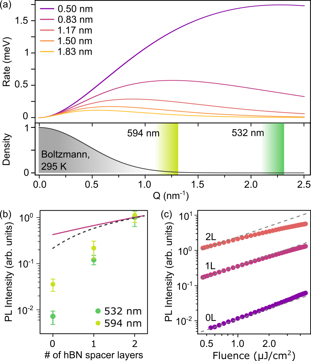
Fig. 4 (b) shows a comparison of the PL intensities for interlayer distances nm for excitation with the two laser sources at the same incident power. An increase of PL intensity of a factor of five is observed for the excitation with the smaller excess energy. This corresponds to a significant reduction of the total transfer rate, which demonstrates that, indeed, the charge carrier distributions substantially influence the effective transfer rates.
Lastly, we describe the quenching at higher excitation densities, at which interactions are expected to play a role, and which are typically employed in time-resolved experiments. We use a supercontinuum laser, filtered to a wavelength of (532 nm, which has a pulse duration of approximately 10 ps and a repetition rate of 80 MHz. In Fig. 4 (c), the PL intensities at 0, 1 and 2 spacer layers are shown as a function of excitation fluence. For two and one spacer layers, we observe the onset of a sub-linear dependence, most likely caused by exciton-exciton annihilation Yuan and Huang (2015). In the region of direct contact (0L), however, the intensity increases slightly super-linearly. We speculate that this is caused by an increased scattering rate, which allows some carriers to reach the light cone, which would otherwise have been transferred to graphene.
The picture which emerges from our study is that, at room temperature, and for interlayer distances above 1 nm, energy transfer is dominated by Förster interactions. The effective transfer rate in this regime can be calculated by thermally averaging the individual (momentum-dependent) transfer probabilities. Therefore, in this regime, the well known distance-4 relation of the transfer rates holds. Below 1 nm interlayer distance, the individual Förster transfer rates become large enough that on average, charge carriers transfer before they fully thermalize. The total transfer rate is then highly dependent on the excitation condition and is affected by the excess energy as well as the excitation density. A contribution from a Dexter transfer is observed at the smallest interlayer distances, and we infer its magnitude to become comparable to the Förster rates at distances of 0.5 nm. We note that the Dexter contribution might depend on the twist angle between the layers. Since our samples were not purposefully aligned, however, we did not observe significant differences between samples.
While we are able to identify and demonstrate different mechanisms leading to the energy transfer at different interlayer distances, below 1 nm, the experimentally observed PL quenching is still larger than expected for the calculated transfer probabilities in Selig et al. (2019a), even assuming unrealistic carrier distributions. One possibility is that dark excitonic states affect the total transfer rates Lin et al. (2023), which were not explicitly included in the theory. It is also possible that a Meitner-Auger type mechanisms contributes to the total transfer, even though the highest excitation densities here are approximately 5 orders of magnitude lower than in the work introducing this mechanism Dong et al. (2023). Further theoretical and experimental studies, which explicitly take into account the dynamics of non-relaxed carriers, are needed to clarify these details.
To conclude, our results establish a picture of the dominant mechanisms of energy transfer in vdW heterostructures at different interlayer distances, which can serve as a basis for the development of devices requiring the transfer of charge and energy, such as optical detectors or solar panels.
The authors thank Ermin Malic and Joshua Thompson for fruitful discussions. This project has received funding from the European Union’s Horizon 2020 research and innovation programme under grant agreement No 881603, by the Deutsche Forschungsgemeinschaft (DFG, German Research Foundation) under Germany’s Excellence Strategy - Cluster of Excellence Matter and Light for Quantum Computing (ML4Q) EXC 2004/1 – 390534769. K.W. and T.T. acknowledge support from the JSPS KAKENHI (Grant Numbers 20H00354, 21H05233 and 23H02052) and World Premier International Research Center Initiative (WPI), MEXT, Japan.
References
- Förster (1949) T. Förster, Zeitschrift für Naturforschung 4, 321 (1949).
- Persson and Lang (1982) B. N. J. Persson and N. D. Lang, Physical Review B 26, 5409 (1982).
- Mirkovic et al. (2017) T. Mirkovic, E. E. Ostroumov, J. M. Anna, R. Van Grondelle, Govindjee, and G. D. Scholes, Chemical Reviews 117, 249 (2017).
- Yang and Neher (2006) X. Yang and D. Neher, Organic Light Emitting Devices: Synthesis, Properties and Applications (2006) pp. 333–367.
- Pollok and Heim (1999) B. A. Pollok and R. Heim, Trends in Cell Biology 9, 57 (1999).
- Chen et al. (2010) Z. Chen, S. Berciaud, C. Nuckolls, T. F. Heinz, and L. E. Brus, ACS Nano 4, 2964 (2010).
- Federspiel et al. (2015) F. Federspiel, G. Froehlicher, M. Nasilowski, S. Pedetti, A. Mahmood, B. Doudin, S. Park, J. O. Lee, D. Halley, B. Dubertret, P. Gilliot, and S. Berciaud, Nano Letters 15, 1252 (2015).
- Treossi et al. (2009) E. Treossi, M. Melucci, A. Liscio, M. Gazzano, P. Samorì, and V. Palermo, Journal of the American Chemical Society 131, 15576 (2009).
- Gaudreau et al. (2013) L. Gaudreau, K. J. Tielrooij, G. E. Prawiroatmodjo, J. Osmond, F. J. De Abajo, and F. H. Koppens, Nano Letters 13, 2030 (2013).
- (10) J. He, N. Kumar, M. Z. Bellus, H. Y. Chiu, D. He, Y. Wang, and H. Zhao, Nature Communications 5, 5622.
- Hill et al. (2017) H. M. Hill, A. F. Rigosi, A. Raja, A. Chernikov, C. Roquelet, and T. F. Heinz, Physical Review B 96, 205401 (2017).
- Froehlicher et al. (2018) G. Froehlicher, E. Lorchat, and S. Berciaud, Physical Review X 8, 011007 (2018).
- Aeschlimann et al. (2020) S. Aeschlimann, A. Rossi, M. Chávez-Cervantes, R. Krause, B. Arnoldi, B. Stadtmüller, M. Aeschlimann, S. Forti, F. Fabbri, C. Coletti, and I. Gierz, Science Advances 6, eaay0761 (2020).
- Georgiou et al. (2013) T. Georgiou, R. Jalil, B. D. Belle, L. Britnell, R. V. Gorbachev, S. V. Morozov, Y. J. Kim, A. Gholinia, S. J. Haigh, O. Makarovsky, L. Eaves, L. A. Ponomarenko, A. K. Geim, K. S. Novoselov, and A. Mishchenko, Nature Nanotechnology 8, 100 (2013).
- Britnell et al. (2013) L. Britnell, R. M. Ribeiro, A. Eckmann, R. Jalil, B. D. Belle, A. Mishchenko, Y.-J. Kim, R. V. Gorbachev, T. Georgiou, S. V. Morozov, A. N. Grigorenko, A. K. Geim, C. Casiraghi, a. H. Castro Neto, and K. S. Novoselov, Science 340, 1311 (2013).
- Zhang et al. (2014) W. Zhang, C. P. Chuu, J. K. Huang, C. H. Chen, M. L. Tsai, Y. H. Chang, C. T. Liang, Y. Z. Chen, Y. L. Chueh, J. H. He, M. Y. Chou, and L. J. Li, Scientific Reports 4, 3826 (2014).
- Bernardi et al. (2013) M. Bernardi, M. Palummo, and J. C. Grossman, Nano Letters 13, 3664 (2013).
- Nassiri Nazif et al. (2021) K. Nassiri Nazif, A. Daus, J. Hong, N. Lee, S. Vaziri, A. Kumar, F. Nitta, M. E. Chen, S. Kananian, R. Islam, K. H. Kim, J. H. Park, A. S. Poon, M. L. Brongersma, E. Pop, and K. C. Saraswat, Nature Communications 12, 7034 (2021).
- Dexter (1953) D. L. Dexter, The Journal of Chemical Physics 21, 836 (1953).
- Swathi and Sebastian (2009) R. S. Swathi and K. L. Sebastian, Journal of Chemical Physics 130, 086101 (2009).
- Malic et al. (2014) E. Malic, H. Appel, O. T. Hofmann, and A. Rubio, Journal of Physical Chemistry C 118, 9283 (2014).
- Selig et al. (2019a) M. Selig, E. Malic, K. J. Ahn, N. Koch, and A. Knorr, Physical Review B 99, 035420 (2019a).
- Krause et al. (2021) R. Krause, S. Aeschlimann, M. Chávez-Cervantes, R. Perea-Causin, S. Brem, E. Malic, S. Forti, F. Fabbri, C. Coletti, and I. Gierz, Physical Review Letters 127, 276401 (2021).
- Dong et al. (2023) S. Dong, S. Beaulieu, M. Selig, P. Rosenzweig, D. Christiansen, T. Pincelli, M. Dendzik, J. D. Ziegler, J. Maklar, R. P. Xian, A. Neef, A. Mohammed, A. Schulz, M. Stadler, M. Jetter, P. Michler, T. Taniguchi, K. Watanabe, H. Takagi, U. Starke, A. Chernikov, M. Wolf, H. Nakamura, A. Knorr, L. Rettig, and R. Ernstorfer, Nature Communications 14, 5057 (2023).
- Britnell et al. (2012) L. Britnell, R. V. Gorbachev, R. Jalil, B. D. Belle, F. Schedin, M. I. Katsnelson, L. Eaves, S. V. Morozov, A. S. Mayorov, N. M. R. Peres, A. H. C. Neto, J. Leist, A. K. Geim, L. A. Ponomarenko, and K. S. Novoselov, Nano Letters 12, 1707 (2012).
- Brotons-Gisbert et al. (2019) M. Brotons-Gisbert, A. Branny, S. Kumar, R. Picard, R. Proux, M. Gray, K. S. Burch, K. Watanabe, T. Taniguchi, and B. D. Gerardot, Nature Nanotechnology 14, 442 (2019).
- Tebbe et al. (2023a) D. Tebbe, M. Schütte, K. Watanabe, T. Taniguchi, C. Stampfer, B. Beschoten, and L. Waldecker, npj 2D Materials and Applications 7, 29 (2023a).
- Uslu et al. (2023) J.-L. Uslu, T. Ouaj, D. Tebbe, A. Nekrasov, J. H. Bertram, M. Schütte, K. Watanabe, T. Taniguchi, B. Beschoten, L. Waldecker, and C. Stampfer, ArXiv e-prints (2023), 2306.14845.
- Rooney et al. (2017) A. P. Rooney, A. Kozikov, A. N. Rudenko, E. Prestat, M. J. Hamer, F. Withers, Y. Cao, K. S. Novoselov, M. I. Katsnelson, R. Gorbachev, and S. J. Haigh, Nano Letters 17, 5222 (2017).
- Pease (1950) R. S. Pease, Nature 165, 722 (1950).
- Haigh et al. (2012) S. J. Haigh, A. Gholinia, R. Jalil, S. Romani, L. Britnell, D. C. Elias, K. S. Novoselov, L. A. Ponomarenko, A. K. Geim, and R. Gorbachev, Nature Materials 11, 764 (2012).
- Tebbe et al. (2023b) D. Tebbe, B. Kundu, B. Beschoten, P. K. Sahoo, and L. Waldecker, (2023b), 10.48550/arXiv.2305.06945.
- Mak et al. (2013) K. F. Mak, K. He, C. Lee, G. H. Lee, J. Hone, T. F. Heinz, and J. Shan, Nature materials 12, 207 (2013).
- Arora et al. (2015) A. Arora, M. Koperski, K. Nogajewski, J. Marcus, C. Faugeras, and M. Potemski, Nanoscale 7, 10421 (2015).
- Raja et al. (2017) A. Raja, A. Chaves, J. Yu, G. Arefe, H. M. Hill, A. F. Rigosi, T. C. Berkelbach, P. Nagler, C. Schüller, T. Korn, C. Nuckolls, J. Hone, L. E. Brus, T. F. Heinz, D. R. Reichman, and A. Chernikov, Nature Communications 8, 15251 (2017).
- (36) See Supplemental Material at [URL will be inserted by publisher] for more information on the normalization of PL intensity, analysis of the minimal linewidth, and the rate equation model for PL quenching.
- Fang et al. (2019) H. H. Fang, B. Han, C. Robert, M. A. Semina, D. Lagarde, E. Courtade, T. Taniguchi, K. Watanabe, T. Amand, B. Urbaszek, M. M. Glazov, and X. Marie, Physical Review Letters 123, 067401 (2019).
- Lorchat et al. (2020) E. Lorchat, L. E. López, C. Robert, D. Lagarde, G. Froehlicher, T. Taniguchi, K. Watanabe, X. Marie, and S. Berciaud, Nature Nanotechnology 15, 283 (2020).
- Raja et al. (2019) A. Raja, L. Waldecker, J. Zipfel, Y. Cho, S. Brem, J. D. Ziegler, M. Kulig, T. Taniguchi, K. Watanabe, E. Malic, T. F. Heinz, T. C. Berkelbach, and A. Chernikov, Nature Nanotechnology 14, 832 (2019).
- Gómez-Santos and Stauber (2011) G. Gómez-Santos and T. Stauber, Physical Review B 84, 165438 (2011).
- Steinhoff et al. (2018) A. Steinhoff, T. O. Wehling, and M. Rösner, Physical Review B 98, 045304 (2018).
- Waldecker et al. (2019) L. Waldecker, A. Raja, M. Rösner, C. Steinke, A. Bostwick, R. J. Koch, C. Jozwiak, T. Taniguchi, K. Watanabe, E. Rotenberg, T. O. Wehling, and T. F. Heinz, Physical Review Letters 123, 206403 (2019).
- Fu et al. (2019) Y. Fu, D. He, J. He, A. Bian, L. Zhang, S. Liu, Y. Wang, and H. Zhao, Advanced Materials Interfaces 6, 1901307 (2019).
- Robert et al. (2016) C. Robert, D. Lagarde, F. Cadiz, G. Wang, B. Lassagne, T. Amand, A. Balocchi, P. Renucci, S. Tongay, B. Urbaszek, and X. Marie, Physical Review B 93, 205423 (2016).
- Brem et al. (2018) S. Brem, M. Selig, G. Berghaeuser, and E. Malic, Scientific Reports 8, 8238 (2018).
- Selig et al. (2019b) M. Selig, F. Katsch, R. Schmidt, S. Michaelis De Vasconcellos, R. Bratschitsch, E. Malic, and A. Knorr, Physical Review Research 1, 022007(R) (2019b).
- Waldecker et al. (2017) L. Waldecker, R. Bertoni, H. Hübener, T. Brumme, T. Vasileiadis, D. Zahn, A. Rubio, and R. Ernstorfer, Physical Review Letters 119, 036803 (2017).
- Yuan and Huang (2015) L. Yuan and L. Huang, Nanoscale 7, 7402 (2015).
- Lin et al. (2023) J. D. Lin, P. Y. Lo, G. H. Peng, W. H. Li, S. Y. Huang, G. Y. Chen, and S. J. Cheng, npj 2D Materials and Applications 7, 65 (2023).