Electron-phonon coupling, critical temperatures and gaps in / Ising superconductors
Abstract
Utilizing Migdal-Eliashberg theory of superconductivity within the first-principles calculations, we work out the role of electron-phonon coupling (EPC) and anisotropic superconducting properties of a recently discovered [PRB 104, 174510 (2021)] 2D van der Waals heterostructure comprising a single layer of MoS2 and few layers of NbSe2. We find strong EPC and a softening of phonon modes in the lowest acoustic branch. While the single MoS2 layer does not actively contribute to the EPC, it significantly elevates the superconducting critical temperature () compared to monolayer NbSe2. This is attributed to the degradation of the charge-density wave (CDW) by the MoS2 layer. Notably, we observe a two-gap superconductivity in / and extend our study to three layers of NbSe2. A reduction in with increasing thickness of NbSe2 is observed. We confirm that this trend is consistent with recent experiments, if one goes beyond three layers of NbSe2. Incorporation of spin-orbit coupling (SOC) suggests a possible mechanism for Ising superconductivity. We find that SOC reduces EPC while is suppressed concomitantly by about 5K, leading to a closer estimate of the experimental .
Charge density wave (CDW) and superconductivity (SC) are competing instabilities in a vast variety of materials such as TMDs [1, 2], intercalated materials, and recently investigated Kagome metals [3]. TMDs have drawn great interest lately due to their device application potential. Apart from their semiconducting, spintronic and valleytronic attributes, TMDs are studied for the competition between CDW and SC [4, 5, 6, 7, 8, 9, 10]. Other than disorder, dimensionality also plays a significant role in manipulating the behaviour of these systems. [11, 12].
Van der Waals heterostructures have captured considerable attention over the past two decades since the discovery of graphene due to the display of unique properties that hold immense promise for electronic and optoelectronic applications. The prospect of crafting a van der Waals heterostructure with intriguing emergent properties appears to be a novel route towards advanced tunable devices. In particular, the transition metal dichalcogenides (TMDs), which are categorized as two-dimensional semiconductors, emerged as noteworthy candidates. Among these, has garnered substantial interest as a potential semiconductor, showcasing Ising superconductivity (ISC) in few-layer samples when subjected to electrostatic gating [13]. Likewise, [14] represents another potential Ising superconductor. and had a long-standing appeal to experimental and theoretical investigators owing to the possible co-existence of CDW and SC [15, 2]. Along with CDW and SC, ferromagnetism is also reported in this material [16], which makes it even more intriguing.
is a well-studied TMD material in which CDW and SC coexist at lower temperatures (CDW at 33K with coexisting SC below 7K) [17]. Electron-phonon coupling (EPC), along with electronic correlation [8], plays a crucial role in determining its instabilities rather than Fermi surface (FS) nesting [11]. The interpocket and intrapocket scatterings across the FS are proposed mechanisms for CDW and SC, respectively, in the monolayer system [18]. is a very well-known member in the TMD-family that has been studied quite extensively due to its large spin-orbit coupling [19] and several other topological, electronic, optical, and catalytic properties.
It is found experimentally that 2D samples of are unstable at ambient conditions. Theoretically also, the high symmetry phase of is predicted to be unstable. There is a transition to a distorted CDW superstructure [11] as the temperature is reduced. In a recent study, ISC is claimed in the heterostacking of a few layers of with a single layer of , where the authors argue in favour of the stability of a 2D SC [20] state. Though the competition between CDW and SC was not addressed, it seems plays a very crucial role in mitigating the effects of CDW, stabilizing the SC state by preventing a clustering of into a CDW superstructure, reported in an earlier study on intercalated bilayers [21].
ISC has gained prominence as a burgeoning field in the search for unconventional SC lately [13, 14, 22, 23]. ISC primarily originates in systems lacking inversion symmetry that leads to an intrinsic SOC. TMDs are the main candidates in which ISC is likely to occur. In these systems, spins align themselves in the out-of-plane direction, and it takes a high in-plane upper critical field to destroy the superconductivity. For these superconductors, the in-plane magnetic field crosses the Chandrasekhar-Clogston-Pauli limit, . Therefore, a considerable influence of SOC on the superconducting properties of Ising superconductors is anticipated. But SOC is not the only factor which affects ISC, spin-orbit scattering [24], singlet-triplet mixing [25], spin-fluctuations [26], disorder [27] and intervalley scattering [28] could affect ISC concurrently. In this work, we will also discuss the effect of SOC on electronic and superconducting properties.
2H polymorphs of and are members of transition metal dichalcogenides (TMDs) family with point group symmetry in which transition metals are sandwiched between the chalcogen layers. We model 2D heterostructures with one layer of and -layers of ( configuration). with lattice constant () of Å works as a substrate which produces % (for 1/1) of tensile strain while stacked with ( Å). The in-plane lattice constants for different layers of are provided in Table T1 of supplementary material (SM) [29]. The negative binding energy [] implies a strong possibility of the formation of / heterostructures as shown in Table T1 of the SM [29]. In the present work, we go up to four layers of that are stacked with in a particular stacking with respect to each other as shown in Fig. 1. It is important to mention that the AB-stacking is used to form the crystal structures, which is found to be the most stable stacking for these hexagonal heterostructures [30]. In AB-stacking, the chalcogen atom and the transition metal atom from different layers are on top of each other vertically along axis. The monolayers of and show semiconducting and metallic properties individually. undergoes a structural transition to CDW phase at finite temperature (33K) and also shows superconducting properties at even lower temperature around 7K [18].
 |
Electronic structure calculations show (See Fig. S1 in the SM [29]) that orbitals of atoms mainly contribute at the Fermi level (FL). The topology of the bands is nearly intact close to the FL and remains the same as for the monolayer. Also, the overall band structure from layer is similar to the pristine monolayer, except the conduction bands are shifted downward and interact with the bands, which clearly indicates interfacial interactions between the two layers at the interface. In the valence band region, one may notice a hybridization between orbitals and orbitals. In the FS plot there are two types of hole pockets, one at the and the other at the point. The emergence of the hole pocket at the point is attributed to Nb and orbitals, whereas the hole pocket at the point arises from the Nb orbital. Increasing the number of layers of has no significant effect on the bands except shifting the MoS2-derived bands downward as they cross the FL eventually for . The reason for this downward shift is the tensile strain induced in the heterostructures with increasing layers [30]. On the other hand, it is obvious that on increasing , more bands populate the FL. The lowest band, which is closer to FL and belongs to the lowest NbSe2 layer, comes closer to FL and becomes flatter, increasing the size of the hole pockets at the point.
We also perform calculations including spin-orbit coupling (SOC). The SOC bands are shown in Fig. S1(c), where one may notice that SOC has a significant effect on bands in all the cases. Despite the significant spin-splitting observed in the bands of , its considerable distance from the FL implies the splitting is not going to alter the physical picture substantially. At the point, the bands at FL have a noticeable Zeeman type spin-splitting. A negligible Rashba spin-splitting can also be seen at the valence band maxima at point in all the cases. This is similar to the case of monolayer . This Rashba type spin-splitting in the bands near the interface is the signature of 2D electron-gas at the interface of and . The presence of SOC in van der Waals materials is pivotal in influencing electron-phonon interactions, which will be discussed later.
 |
To calculate the phonon-mediated superconducting properties of the layered / heterostructure, we first calculate the dynamical matrices using density functional perturbation theory as implemented in QE. There is no visible gap in the spectrum over the whole frequency range. However, from the partial density of states it is clear that the lowest few phonon modes (acoustic) are contributed by Nb (the red curve in the phonon DOS for 1/1 of Fig. 2(d)), followed by a gap in the range between to meV for the Nb modes. All the modes coming from Nb in systems with are equally populated in the acoustic phonon region in the range from to meV, as shown in Figs. 2(a-c). There is a finite but very small contribution of Mo atom to the acoustic modes in comparison to contributions from NbSe2. The optical branches are coming mainly from S, and the Mo atom has a substantial contribution in the higher frequency regime. There is a small hybridization of Se with Nb in the acoustic modes, which suggests that the NbSe2 layers play a substantial role in EPC. One can also note that beyond meV, neither Nb nor Se contributes to the optical branches, and it will be more explicit in the spectral function plot shown in Fig. 3, that, beyond meV, vanishes. This implies NbSe2 layers only are responsible for EPC and electron-phonon induced SC. The plots of mode-resolved in the SM vindicates this clearly. These plots and details thereof are provided in Fig. S1 of SM [29]. To be sure of the source of EPC, mode-resolved electron-phonon linewidth plots are also shown in Fig. 2, using the relation [31, 32],
| (1) |
The parameters are defined in the computational details section of the SM [29]. One can clearly observe a phonon-softening in between and high-symmetry points in the LA phonon branch, which is known to be vibrational mode of the acoustic branch. This mode belongs to the NbSe2 layer and indicates the movement of Nb and two Se atoms in the same in-plane direction. It is interesting to point out that in monolayer NbSe2, this phonon-softening occurs at a q point where, q [18, 33], implying a CDW instability. In the case of 1/1-NbSe2/MoS2, we observe it at q (Fig. 2(a)), suggesting a commensurate CDW ordering. As the number of NbSe2 layers increases, the softening approaches q gradually, possibly through a series of incommensurate CDWs, at least for 2/1 and 3/1 configurations. The color scale suggests that almost all the EPC is concentrated in this phonon-softening valley of the acoustic branch of NbSe2, and the other modes do not contribute to EPC. This is true for all the three cases 2(a-c). A similar softening is also found in bare NbSe2 monolayer [18]; the only difference is that the softening in our case is between and points while it is close to the point in the earlier study, indicating that a single layer of MoS2 affects the EPC strength in NbSe2/MoS2 heterostructures.
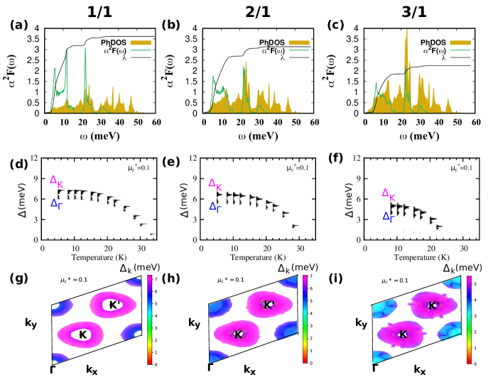
Next we calculate EPC strength, , as a function of frequency and show in Fig 3(a) along with Eliashberg spectral function . vanishes beyond meV. Comparison of with partial DOS (in Fig. 2(d-f)) shows that the contribution from NbSe2 layers also vanishes beyond this range; that means NbSe2 layers are sole contributors to EPC. The also behaves in the same manner as the partial DOS in the range meV. The gaps in in the range meV and meV in Fig. 3(a-c) are apparent from the partial DOS of Nb and Se in Fig. 2(d-f). The cumulative EPC, indicated by in Figs. 3(a-c), is calculated using Eqn. (2), described in the SM [29]. Clearly, reduces from to as the NbSe2 layer numbers increase from 1 to 3 (i.e., 1/1 to 3/1 heterostructure) respectively, due to the reduction of . This reduction in total EPC will also result in the reduction of . A sudden jump in at a frequency, meV is noticed in all three cases, due to a gap opening in the spectral function between acoustic and optical phonon modes of Nb.
To evaluate the superconducting , fully anisotropic Migdal-Eliashberg theory [34, 31] is employed. Fig. 3(d-f) show the energy distribution of the superconducting gap as a function of temperature at an effective Coulomb potential . The leading edge of the gap function () at K is at 6.7 meV. The ordinary Allen-Dynes modified McMillan equation [35] gives a superconducting K, while anisotropic Migdal-Eliashberg theory gives K. This large difference in the two superconducting is a signature of anisotropy in the superconducting gap distribution on the FS, which is a consequence of the multi-sheet nature of FS in NbSe2/MoS2. This was observed [31] in MgB2 (K) too, which is a two-gap superconductor. In NbSe2/MoS2, there are hole-pockets around , and valleys in the BZ. The larger gap is associated with the out-of-plane Fermi-sheets at the point, while the smaller gap involves in-plane Nb and Fermi-sheets located around the point, shown in the gap-resolved FS in Figs. 3(g-i).It is interesting to note that the two-gap feature is robust with increasing number of NbSe2 layers.
The calculated of NbSe2/MoS2 is large as compared to a single layer of NbSe2. The experimental value is 3.8K for the single layer system [36], while it is 7K for bulk NbSe2 [37]. An EPW calculation on a 3x3 CDW supercell reported = 4.4K for a single layer [18]. Thus, our study suggests that a single layer of MoS2 has a substantial impact on SC of 2H-NbSe2. Increasing the number of NbSe2 layers up to three shows a constant reduction in in Figs. 3(d-f) and in Table 1. is sensitive to the choice of Coulomb potential (). An increase in results in a decrease in superconducting and [31]. Since there are no available estimates of to compare with, we have calculated for different values of (Table. 1).
ISC with K has been suggested in a single layer of MoS2 stacked with few layers of NbSe2 (15 nm, to be exact) [20, 38] recently. A similar is expected with increasing NbSe2 layers. The variation of with the thickness of NbSe2 suggests an increase in NbSe2 layers will result in a suppression of as shown in scanning tunneling microscopy measurements [39]. Migdal-Eliashberg theory, incorporating spin-fluctuations, finds this trend for 1H-TaS2 [33] and more recently in 2H-NbSe2 [26]. In 1H-TaS2, it is attributed to an inevitable suppression of Cooper pair density at the superconductor-vacuum interface. Our computational resources make it difficult to go beyond three layers of NbSe2, however the trend is clear.
| (K) | |||
|---|---|---|---|
| 1/1 | 2/1 | 3/1 | |
| 0.05 | 37.4 | 34.1 | 28.7 |
| 0.10 | 35.3 | 31.0 | 24.0 |
| 0.16 | 30.1 | 27.9 | 21.3 |
Furthermore, it is important to emphasize that the Migdal-Eliashberg approach results in a fair agreement for a variety of materials, though it overestimates the superconducting gap and [40, 25, 26]. The claim is that in NbSe2 and similar materials that show ISC, the overestimation of phonon-induced SC can be mitigated by spin-fluctuations [25, 26]. For a comparison, we perform the EPW calculations for the NbSe2 monolayer and find an overestimated K as reported earlier [26]. The same could be possible for NbSe2/MoS2 heterostructures.
Finally, speaking of ISC, a mechanism which is controlled by SOC in non-centrosymmetric materials, we infer that the SOC, which has been ignored in electron-phonon calculations so far, can have a huge impact on the EPC strength. Inclusion of SOC weakens the EPC strength almost by a factor of two as reported earlier in the case of CaBi2 [41] and TaS2 [33], close to the experimentally reported values. system exhibits a notable SOC as illustrated in Fig. S1(c), which is evident from a Zeeman type of spin-splitting at the point in the BZ. Considering this, incorporating SOC into calculations may yield a more accurate estimate of . Including SOC, the superconducting is indeed reduced by about 5K for 1/1 (K, ) and 2/1-NbSe2/MoS2 (K, ) as shown in Fig. S3 of SM [29]. More experimental investigations should provide a better estimate of in () and validate our results.
To summarize, we investigated electronic and superconducting properties of AB-stacked NbSe2/MoS2 van der Waals heterostructures and studied the behavior of critical temperature with the number of layers of NbSe2, using Migdal-Eliashberg theory. While NbSe2 layers affect the FL considerably, a single layer of MoS2 does not significantly alter the FS topology, at least up to 4/1 configuration. Moreover, the heterostructure shows a robust electron-phonon coupling (EPC) strength. A pronounced phonon softening in the acoustic modes of the NbSe2 layers is observed along the direction, attributed to movements of Nb and Se atoms within the -plane. MoS2 layers do not exhibit any EPC, though their inclusion dramatically enhances the when stacked with NbSe2. This enhancement owes its origin to the stabilization of the crystal structure by MoS2, mitigating the CDW instability of NbSe2. Our findings suggest a substantial increase in when a semiconducting 2D material like MoS2 is combined with a superconducting counterpart like NbSe2. We also suggest that increasing the thickness of NbSe2, stacked with a single layer of MoS2, results in an unusual reduction in . We anticipate that the experimentally reported could be attained by adding more (beyond 4) layers of NbSe2. Additionally, we observe that the inclusion of spin-orbit coupling (SOC) leads to a marked decrease in EPC, significantly degrading . This also points to the possibility of an Ising superconductivity in this system.
We acknowledge National Supercomputing Mission (NSM) for providing computing resources of ’PARAM Shakti’ at IIT Kharagpur, which is implemented by C-DAC and supported by the Ministry of Electronics and Information Technology (MeitY) and Department of Science and Technology (DST), Government of India.
References
- [1] Miguel M Ugeda, Aaron J Bradley, Yi Zhang, Seita Onishi, Yi Chen, Wei Ruan, Claudia Ojeda-Aristizabal, Hyejin Ryu, Mark T Edmonds, Hsin-Zon Tsai, et al. Characterization of collective ground states in single-layer NbSe2. Nature Physics, 12(1):92–97, 2016.
- [2] Sudipta Koley, Narayan Mohanta, and A Taraphder. Charge density wave and superconductivity in transition metal dichalcogenides. The European Physical Journal B, 93:1–8, 2020.
- [3] FH Yu, DH Ma, WZ Zhuo, SQ Liu, XK Wen, Bin Lei, JJ Ying, and XH Chen. Unusual competition of superconductivity and charge-density-wave state in a compressed topological kagome metal. Nature communications, 12(1):3645, 2021.
- [4] G. Grüner. The dynamics of charge-density waves. Rev. Mod. Phys., 60:1129–1181, Oct 1988.
- [5] S. V. Borisenko, A. A. Kordyuk, V. B. Zabolotnyy, D. S. Inosov, D. Evtushinsky, B. Büchner, A. N. Yaresko, A. Varykhalov, R. Follath, W. Eberhardt, L. Patthey, and H. Berger. Two Energy Gaps and Fermi-Surface "Arcs" in . Phys. Rev. Lett., 102:166402, Apr 2009.
- [6] R. E. Thomson, B. Burk, A. Zettl, and John Clarke. Scanning tunneling microscopy of the charge-density-wave structure in 1T-. Phys. Rev. B, 49:16899–16916, Jun 1994.
- [7] F. Weber, S. Rosenkranz, J.-P. Castellan, R. Osborn, R. Hott, R. Heid, K.-P. Bohnen, T. Egami, A. H. Said, and D. Reznik. Extended Phonon Collapse and the Origin of the Charge-Density Wave in 2H-NbSe2. Phys. Rev. Lett., 107:107403, Sep 2011.
- [8] SV Dordevic, DN Basov, RC Dynes, B Ruzicka, V Vescoli, L Degiorgi, H Berger, R Gaál, L Forró, and E Bucher. Optical properties of the quasi-two-dimensional dichalcogenides 2H-TaSe and 2H-NbSe. The European Physical Journal B-Condensed Matter and Complex Systems, 33:15–23, 2003.
- [9] A. Taraphder, S. Koley, N. S. Vidhyadhiraja, and M. S. Laad. Preformed Excitonic Liquid Route to a Charge Density Wave in 2H-TaSe2. Phys. Rev. Lett., 106:236405, Jun 2011.
- [10] S. Koley, M. S. Laad, N. S. Vidhyadhiraja, and A. Taraphder. Preformed excitons, orbital selectivity, and charge density wave order in 1T-TiSe2. Phys. Rev. B, 90:115146, Sep 2014.
- [11] Matteo Calandra, I. I. Mazin, and Francesco Mauri. Effect of dimensionality on the charge-density wave in few-layer . Phys. Rev. B, 80:241108, Dec 2009.
- [12] Chao-Sheng Lian. Interplay of charge ordering and superconductivity in two-dimensional group V transition-metal dichalcogenides. Phys. Rev. B, 107:045431, Jan 2023.
- [13] JM Lu, O Zheliuk, Inge Leermakers, Noah FQ Yuan, Uli Zeitler, Kam Tuen Law, and JT3445699 Ye. Evidence for two-dimensional Ising superconductivity in gated MoS2. Science, 350(6266):1353–1357, 2015.
- [14] Xiaoxiang Xi, Zefang Wang, Weiwei Zhao, Ju-Hyun Park, Kam Tuen Law, Helmuth Berger, László Forró, Jie Shan, and Kin Fai Mak. Ising pairing in superconducting NbSe2 atomic layers. Nature Physics, 12(2):139–143, 2016.
- [15] D. C. Freitas, P. Rodière, M. R. Osorio, E. Navarro-Moratalla, N. M. Nemes, V. G. Tissen, L. Cario, E. Coronado, M. García-Hernández, S. Vieira, M. Núñez-Regueiro, and H. Suderow. Strong enhancement of superconductivity at high pressures within the charge-density-wave states of 2H-TaS2 and 2H-TaSe2. Phys. Rev. B, 93:184512, May 2016.
- [16] Xiaojiao Zhu, Yuqiao Guo, Hao Cheng, Jun Dai, Xingda An, Jiyin Zhao, Kangzhen Tian, Shiqiang Wei, Xiao Cheng Zeng, Changzheng Wu, et al. Signature of coexistence of superconductivity and ferromagnetism in two-dimensional NbSe2 triggered by surface molecular adsorption. Nature communications, 7(1):11210, 2016.
- [17] Xiaoxiang Xi, Liang Zhao, Zefang Wang, Helmuth Berger, László Forró, Jie Shan, and Kin Fai Mak. Strongly enhanced charge-density-wave order in monolayer NbSe2. Nature nanotechnology, 10(9):765–769, 2015.
- [18] Feipeng Zheng and Ji Feng. Electron-phonon coupling and the coexistence of superconductivity and charge-density wave in monolayer . Phys. Rev. B, 99:161119, Apr 2019.
- [19] Z. Y. Zhu, Y. C. Cheng, and U. Schwingenschlögl. Giant spin-orbit-induced spin splitting in two-dimensional transition-metal dichalcogenide semiconductors. Phys. Rev. B, 84:153402, Oct 2011.
- [20] Prakiran Baidya, Divya Sahani, Hemanta Kumar Kundu, Simrandeep Kaur, Priya Tiwari, Vivas Bagwe, John Jesudasan, Awadhesh Narayan, Pratap Raychaudhuri, and Aveek Bid. Transition from three- to two-dimensional Ising superconductivity in few-layer by proximity effect from van der Waals heterostacking. Phys. Rev. B, 104:174510, Nov 2021.
- [21] Yuguo Yin, Chao-Sheng Lian, Fanqi Meng, Yaowu Liu, Wei Chen, Lichen Ji, Xinyu Zhou, Zichun Zhang, Qinghua Zhang, Lin Gu, Wenhui Duan, Qi-Kun Xue, Xi Chen, and Shuai-Hua Ji. Quenched charge density wave and large in-plane upper critical field of self-intercalated bilayer . Phys. Rev. B, 108:L041405, Jul 2023.
- [22] Sergio C De la Barrera, Michael R Sinko, Devashish P Gopalan, Nikhil Sivadas, Kyle L Seyler, Kenji Watanabe, Takashi Taniguchi, Adam W Tsen, Xiaodong Xu, Di Xiao, et al. Tuning ising superconductivity with layer and spin–orbit coupling in two-dimensional transition-metal dichalcogenides. Nature communications, 9(1):1427, 2018.
- [23] Benjamin T. Zhou, Noah F. Q. Yuan, Hong-Liang Jiang, and K. T. Law. Ising superconductivity and Majorana fermions in transition-metal dichalcogenides. Phys. Rev. B, 93:180501, May 2016.
- [24] R. V. Coleman, G. K. Eiserman, S. J. Hillenius, A. T. Mitchell, and J. L. Vicent. Dimensional crossover in the superconducting intercalated layer compound -Ta. Phys. Rev. B, 27:125–139, Jan 1983.
- [25] Darshana Wickramaratne, Sergii Khmelevskyi, Daniel F. Agterberg, and I. I. Mazin. Ising Superconductivity and Magnetism in . Phys. Rev. X, 10:041003, Oct 2020.
- [26] S. Das, H. Paudyal, E. R. Margine, D. F. Agterberg, and I. I. Mazin. Electron-phonon coupling and spin fluctuations in the Ising superconductor NbSe2. npj Computational Materials, 9(1):66, 2023.
- [27] David Möckli and Maxim Khodas. Ising superconductors: Interplay of magnetic field, triplet channels, and disorder. Phys. Rev. B, 101:014510, Jan 2020.
- [28] Stefan Ilić, Julia S. Meyer, and Manuel Houzet. Enhancement of the upper critical field in disordered transition metal dichalcogenide monolayers. Phys. Rev. Lett., 119:117001, Sep 2017.
- [29] See the supplementary material for computational details, and which contains Refs. [42, 43, 44, 45, 46, 47, 48, 49, 50, 51, 52, 53]. The electronic structures and the mode-resolved spectral function plots are shown in detail. The plots of superconducting gap functions with SOC are also provided.
- [30] Shubham Patel, Urmimala Dey, Narayan Prasad Adhikari, and A. Taraphder. Electric field and strain-induced band-gap engineering and manipulation of the Rashba spin splitting in Janus van der Waals heterostructures. Phys. Rev. B, 106:035125, Jul 2022.
- [31] E. R. Margine and F. Giustino. Anisotropic Migdal-Eliashberg theory using Wannier functions. Phys. Rev. B, 87:024505, Jan 2013.
- [32] Hyungjun Lee, Samuel Poncé, Kyle Bushick, Samad Hajinazar, Jon Lafuente-Bartolome, Joshua Leveillee, Chao Lian, Francesco Macheda, Hari Paudyal, Weng Hong Sio, et al. Electron-phonon physics from first principles using the EPW code. Nature Computational Materials, 2023.
- [33] Chao-Sheng Lian, Christoph Heil, Xiaoyu Liu, Chen Si, Feliciano Giustino, and Wenhui Duan. Intrinsic and doping-enhanced superconductivity in monolayer 1H- TaS2: Critical role of charge ordering and spin-orbit coupling. Phys. Rev. B, 105:L180505, May 2022.
- [34] Samuel Poncé, Elena R Margine, Carla Verdi, and Feliciano Giustino. EPW: Electron–phonon coupling, transport and superconducting properties using maximally localized Wannier functions. Computer Physics Communications, 209:116–133, 2016.
- [35] P. B. Allen and R. C. Dynes. Transition temperature of strong-coupled superconductors reanalyzed. Phys. Rev. B, 12:905–922, Aug 1975.
- [36] R. F. Frindt. Superconductivity in Ultrathin Nb Layers. Phys. Rev. Lett., 28:299–301, Jan 1972.
- [37] Huixia Luo, Judyta Strychalska-Nowak, Jun Li, Jing Tao, Tomasz Klimczuk, and Robert J Cava. S-shaped suppression of the superconducting transition temperature in Cu-intercalated NbSe2. Chemistry of Materials, 29(8):3704–3712, 2017.
- [38] Prakiran Baidya, Vivas Bagwe, Pratap Raychaudhuri, and Aveek Bid. Correlated carrier dynamics in a superconducting van der waals heterostructure. Applied Physics Letters, 120(18), 2022.
- [39] Ekaterina Khestanova, John Birkbeck, Mengjian Zhu, Yang Cao, GL Yu, Davit Ghazaryan, Jun Yin, Helmuth Berger, Laszlo Forro, Takashi Taniguchi, et al. Unusual suppression of the superconducting energy gap and critical temperature in atomically thin NbSe2. Nano letters, 18(4):2623–2629, 2018.
- [40] Maxime Leroux, Ion Errea, Mathieu Le Tacon, Sofia-Michaela Souliou, Gaston Garbarino, Laurent Cario, Alexey Bosak, Francesco Mauri, Matteo Calandra, and Pierre Rodiere. Strong anharmonicity induces quantum melting of charge density wave in 2H-NbSe2 under pressure. Phys. Rev. B, 92(14):140303, Oct 2015.
- [41] Sylwia Gołąb and Bartłomiej Wiendlocha. Electron-phonon superconductivity in CaBi2 and the role of spin-orbit interaction. Phys. Rev. B, 99(10):104520, Mar 2019.
- [42] John P. Perdew, Kieron Burke, and Matthias Ernzerhof. Generalized gradient approximation made simple. Phys. Rev. Lett., 77:3865–3868, Oct 1996.
- [43] P. E. Blöchl. Projector augmented-wave method. Phys. Rev. B, 50:17953–17979, Dec 1994.
- [44] G. Kresse and D. Joubert. From ultrasoft pseudopotentials to the projector augmented-wave method. Phys. Rev. B, 59:1758–1775, Jan 1999.
- [45] Stefan Grimme. Semiempirical GGA-type density functional constructed with a long-range dispersion correction. Journal of computational chemistry, 27(15):1787–1799, 2006.
- [46] N. Troullier and José Luís Martins. Efficient pseudopotentials for plane-wave calculations. Phys. Rev. B, 43:1993–2006, Jan 1991.
- [47] Paolo Giannozzi, Stefano Baroni, Nicola Bonini, Matteo Calandra, Roberto Car, Carlo Cavazzoni, Davide Ceresoli, Guido L Chiarotti, Matteo Cococcioni, Ismaila Dabo, et al. QUANTUM ESPRESSO: a modular and open-source software project for quantum simulations of materials. Journal of physics: Condensed matter, 21(39):395502, 2009.
- [48] Paolo Giannozzi, Oliviero Andreussi, Thomas Brumme, Oana Bunau, M Buongiorno Nardelli, Matteo Calandra, Roberto Car, Carlo Cavazzoni, Davide Ceresoli, Matteo Cococcioni, et al. Advanced capabilities for materials modelling with quantum espresso. Journal of physics: Condensed matter, 29(46):465901, 2017.
- [49] Paolo Giannozzi, Oscar Baseggio, Pietro Bonfà, Davide Brunato, Roberto Car, Ivan Carnimeo, Carlo Cavazzoni, Stefano De Gironcoli, Pietro Delugas, Fabrizio Ferrari Ruffino, et al. Quantum espresso toward the exascale. The Journal of chemical physics, 152(15):154105, 2020.
- [50] Feliciano Giustino, Marvin L. Cohen, and Steven G. Louie. Electron-phonon interaction using Wannier functions. Phys. Rev. B, 76:165108, Oct 2007.
- [51] Philip B Allen and Božidar Mitrović. Theory of superconducting tc. Solid state physics, 37:1–92, 1983.
- [52] W. L. McMillan. Transition Temperature of Strong-Coupled Superconductors. Phys. Rev., 167:331–344, Mar 1968.
- [53] Koichi Momma and Fujio Izumi. VESTA3 for three-dimensional visualization of crystal, volumetric and morphology data. Journal of applied crystallography, 44(6):1272–1276, 2011.