Intrinsic spin Hall effect in 5 metals calculated from ab-initio transport theory
Abstract
We describe how the spin Hall effect (SHE) can be studied from ab-initio by combining density functional theory with the non-equilibrium Green’s functions technique for quantum transport into the so-called DFT+NEGF method. After laying down our theoretical approach, in particular discussing how to compute charge and spin bond currents, DFT+NEGF calculations are carried out for ideal clean systems. In these the transport is ballistic and the linear response limit is met. The SHE emerges in a central region attached to two leads when we apply a bias voltage so that electrons are accelerated by a uniform electric field. As a result, we obtain a finite spin-Hall current and, by performing a scaling analysis with respect to the system size, we estimate the “ballistic” spin Hall conductivity (SHC). We consider metals with fcc and bcc crystal structures, finding that the SHC exhibits a rough qualitative dependence on the -band filling, and comment on these results in relation to existing literature. Finally, within the same DFT+NEGF approach, we also predict the appearance of a current-induced spin dipole moment inside the materials’ unit cell and estimate its magnitude.
I Introduction
The spin-Hall effect (SHE) in non-magnetic conductive materials refers to the generation of a spin current, transverse to the flowing charge current [1, 2]. It arises from the spin-orbit coupling (SOC) and appears as a spin accumulation at the samples’ boundaries [3, 4]. The SHE was first predicted over 50 years ago [5, 6] and later rediscovered and theoretically studied in both metals and semiconductors [7, 8, 9, 10, 11, 12, 13]. It was then experimentally measured about two decades ago [3, 4, 14, 15, 16], ushering a large interest for spintronics-based device applications [17, 18].
The most studied material systems for the SHE are heavy metals with large SOC, such as Pt and W [19, 20, 21, 22, 23, 24, 25, 26, 27, 28]. The common parameters used for quantifying the strength of the SHE are the spin-Hall conductivity (SHC) and the spin-Hall angle (SHA) [1, 29], the latter being conventionally defined as the ratio of the SHC to the longitudinal charge conductivity. SHC and SHA measure the efficiency of a material at generating a spin current and, as such, the discovery of materials with large SHC/SHA has become a sought-after target for the development of high performing SHE-based devices. In this work we describe a theoretical framework to compute these parameters from ab initio.
Originally, the SHE was explained in terms of spin-dependent scattering at impurities, namely it was believed to be an entirely extrinsic effect [5, 7]. However, it was later realized that the SHE also exists as a bulk band-structure effect in many non-magnetic materials with appreciable SOC (i.e., intrinsic SHE) [9, 10]. The current view is then that both intrinsic and extrinsic contributions affect the results of experiments in a complex and often not fully understood manner. Notably, even in those metals, such as Pt, where the SHE is attributed to the intrinsic contribution [30, 31, 32, 33, 34, 35], the reported SHC and SHA still vary widely across different measures [1, 19] with the results that depend on the samples’ crystalline quality and on the presence of unavoidable impurities. These are factors, which altogether remain difficult to characterize [36]. Moreover, it is important to bear in mind that, in experiments, the SHC can only be extrapolated indirectly, after rather complex fitting procedures based on models, since the spin currents, unlike the charge currents, are not directly observable quantities. The SHE thus manifests itself as a surface spin accumulation, which can be probed in optical experiments [3, 4], but can not directly be measured in a device. Furthermore, the SHE is generally accompanied by other charge-to-spin conversion phenomena [37], most notably the so-called Rashba-Edelstein or inverse spin-galvanic effect (ISGE) [38, 39]. This generates an additional spin-polarization of the conduction electrons induced by the charge current. Separating such current-induced spin-polarization from the spin accumulation due to the SHE remains a challenging task and a debated problem [40, 41, 42, 43, 44].
Withstanding these practical as well as fundamental issues, ab-initio calculations have taken a significant role in the study of the SHE [45, 46, 47, 48, 49, 50]. Most works to date rely on two complementary linear-response transport approaches, namely the Boltzmann equation and the Kubo formalism, both using the electronic structure obtained from Kohn-Sham (KS) density functional theory (DFT) [51]. The Boltzmann transport equation is employed for elemental metals with point impurities and thermal disorder, and gives SHC values in the diffusive transport regime. In contrast, the Kubo formalism is generally applied for calculating the intrinsic SHC of bulk materials in terms of the Berry curvature of the energy bands [52, 31, 53, 54, 55, 56, 57].
Despite their respective successes, the Boltzmann transport equation and the Kubo formalism treat opposite physical limits, so that a systematic study of the interplay and competition between the intrinsic and extrinsic SHE remains problematic. In this regard, a valuable alternative approach is scattering theory, where one studies electron and spin transport properties through a finite-sized central region placed between two semi-infinite current/voltage leads with well-defined in- and out-propagating electronic states [58]. The approach coincides with the Landauer-Büttiker formalism for phase coherent transport [59, 60, 61], and the Ohmic limit can be recovered by averaging the results for cells of appropriate size over different disorder realizations [62]. Furthermore, effects due to interfaces, as present in actual devices, are naturally included [48]. To date, scattering theory calculations for the SHE have used a linear-response implementation based on wave functions, which are matched at the boundaries between the central region and the leads [63, 64]. The corresponding results have focused on the Ohmic transport regime, eventually recovering the temperature dependence of both the longitudinal conductivity and the SHC observed in experiments [65, 66].
Scattering theory can be implemented in a more versatile way by using the non-equilibrium Green’s functions (NEGF) technique [67] rather than matching wave-functions. The combination of NEGF with DFT is then generally called DFT+NEGF [68, 69]. On the one hand, when using wave-functions, the details of the central region’s electronic structure are not readily available, since the current through a system is determined solely from the asymptotic states in the current/voltage electrodes. On the other hand, in DFT+NEGF, one obtains simultaneously both those electronic structure details and the transport coefficients, understating the relation between them. Specifically, DFT+NEGF enables us to describe how the density of states, the charge density, the magnetic moments, and other microscopic quantities are modified by presence of a flowing charge current. This means that, in principle, one can describe the SHE and other charge-spin conversion phenomena, such as the ISGE, on an equal footing. In addition to that, DFT+NEGF is also applicable away from the linear-response regime and can be systematically combined with many-body methods, such as dynamical mean-field theory, to describe correlation effects beyond the effective single-particle DFT picture [70, 71]. The NEGF technique was applied to understand the SHE already in early model studies [72, 73, 74]. However, to our knowledge, the use of the NEGF for ab-initio simulations of the SHE remains limited. Only very recently, a study by Belashchenko et al. [75] was dedicated to the SHE in Pt. The objective of our work is to further close this knowledge gap in the application of DFT+NEGF for the SHE and other concomitant charge-to-spin conversion phenomena.
In this work, we explain how to implement and apply state-of-the-art DFT+NEGF for simulating the SHE and computing the SHCs. We focus only on the linear-response limit for ideal clean systems, in order to provide an assessment of the performance of our approach and to discuss the underlying assumptions. In particular, we note that our DFT+NEGF calculations entail a convenient steady-state description of the intrinsic SHE, which is not allowed within the Kubo formalism. It therefore requires a change of perspective in treating the phenomenon.
In our implementation of DFT+NEGF, charge and spin currents are computed via the so-called “bond currents approach” [74, 76, 77, 48, 62, 78, 79, 80], which will be explained in detail here. The calculations are carried out to extract the SHC of the metals with fcc or bcc structure, which show isotropic SHE, meaning that the SHC does not depend on the crystal orientation. In particular, we discuss in great detail the results for Pt, which is found to have the largest value of the SHC, as expected based on both experimental and theoretical literature. We further compare our approach and some of our results to those contained in the recent NEGF-based work by Belashchenko et al. [75], although we stress that our interest is in the ballistic transport regime, while those authors studied the Ohmic limit instead. Finally, we demonstrate that DFT+NEGF can also describe current-induced modifications of the spin density. The ISGE, understood as global spin-polarization of the conduction electrons, is forbidden by symmetry in bcc and fcc materials. Nonetheless, we predict that a spin dipole moment appears over the unit cell of these materials as the charge current breaks time-reversal invariance. As such, our approach can be used to estimate the relative magnitude and the interplay between the SHE and other charge-to-spin conversion effects.
The paper is organized as follows. In Section II, we describe the DFT+NEGF formalism, reviewing the method (Section II.2) and introducing the bond currents approach (Section II.3). In Section III, we provide the computational details of the calculations and in Section IV we present our results. In particular, we first describe the calculations for Pt and then those for other fcc and bcc metals. In Section IV.3, we analyse the current-induced spin dipole. Finally, we conclude in Section V.
II Theoretical framework
We describe here how DFT+NEGF is applied to study the intrinsic SHE. The problem is intuitively rather simple, as one just has to compute longitudinal charge currents and transverse spin currents in a ballistic, namely impurity-free, conductor by using the standard implementation of the method. However, some care is needed at the conceptual level. In fact, our approach relies on a physical picture rather different from that underlying the description of the SHE within the Kubo formalism. As such, we start this section by presenting a few qualitative considerations, which help to understand the associated change of perspective. We leave the presentation of the DFT+NEGF equations for the second part of the section.
II.1 Intrinsic SHE in the steady state
In the study of the intrinsic SHE based on the Kubo’s formalism, one applies an external uniform electric field to an extended ballistic system, and calculates a steady-state spin Hall current in the zero-frequency limit. The coefficient between the electric field and the transverse Hall current is interpreted as the intrinsic part of the static SHC, . In the presence of scattering and finite Drude charge conductivity, that intrinsic SHC will stay independent of the scattering as long as the electric field can be considered uniform compared to the mean free path.
This standard way of analyzing the intrinsic SHE has an obvious physical problem, namely an extended ballistic conductor subject to a static uniform electric field is never stationary. The conduction electrons are accelerated continuously, and the longitudinal response diverges. In fact, in the frequency domain, the longitudinal conductivity grows as and thus, it diverges in the static limit. In contrast, remains finite, making the intrinsic SHA, undefined. This apparent problem reflects the specific physics of the intrinsic SHE in ballistic conductors, that is the spin Hall current is produced only by accelerated electrons. A Gedanken non-equilibrium state of an ideal conductor, in which the conduction electrons have reached a steady-state motion after the application of an electric field pulse, has zero steady-state Hall current, while it is characterized by a non-zero spin polarization equal to the spin transferred across the unit cell during the transient time of the accelerated motion. In this sense the intrinsic Hall current produced by a uniform electric field in the infinite ballistic conductor is, by its nature, a transient phenomenon that can not be described consistently using a steady-state formalism. However, this conceptual problem does not subsist when a uniform electric field is applied only inside a finite region, as is the case in DFT+NEGF transport calculations.
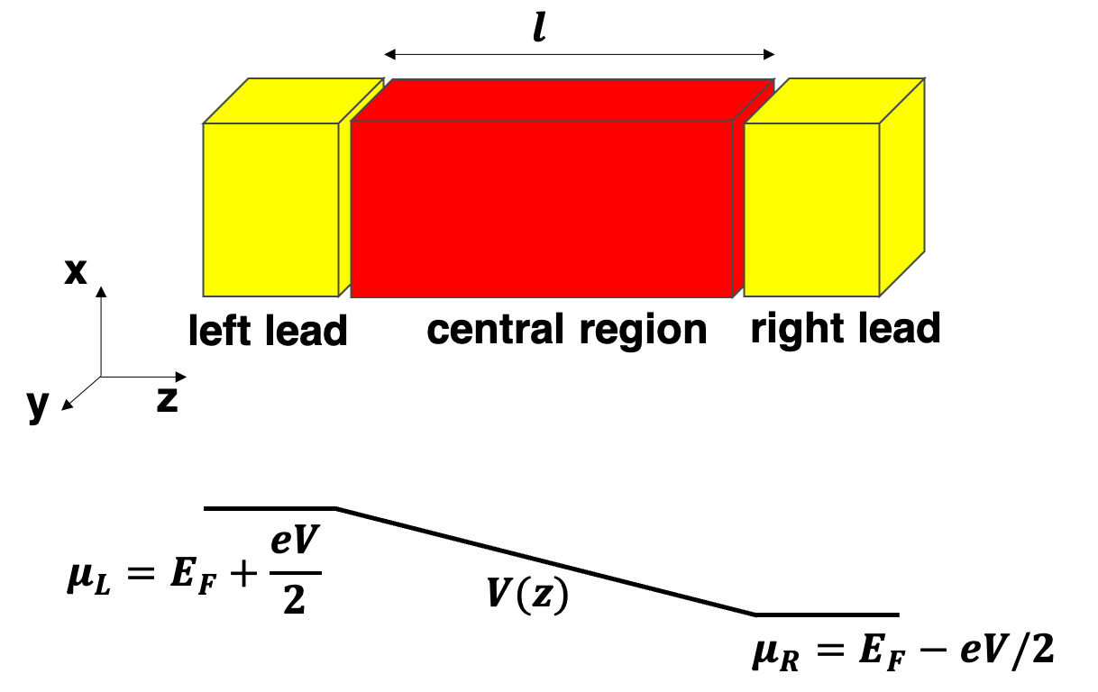
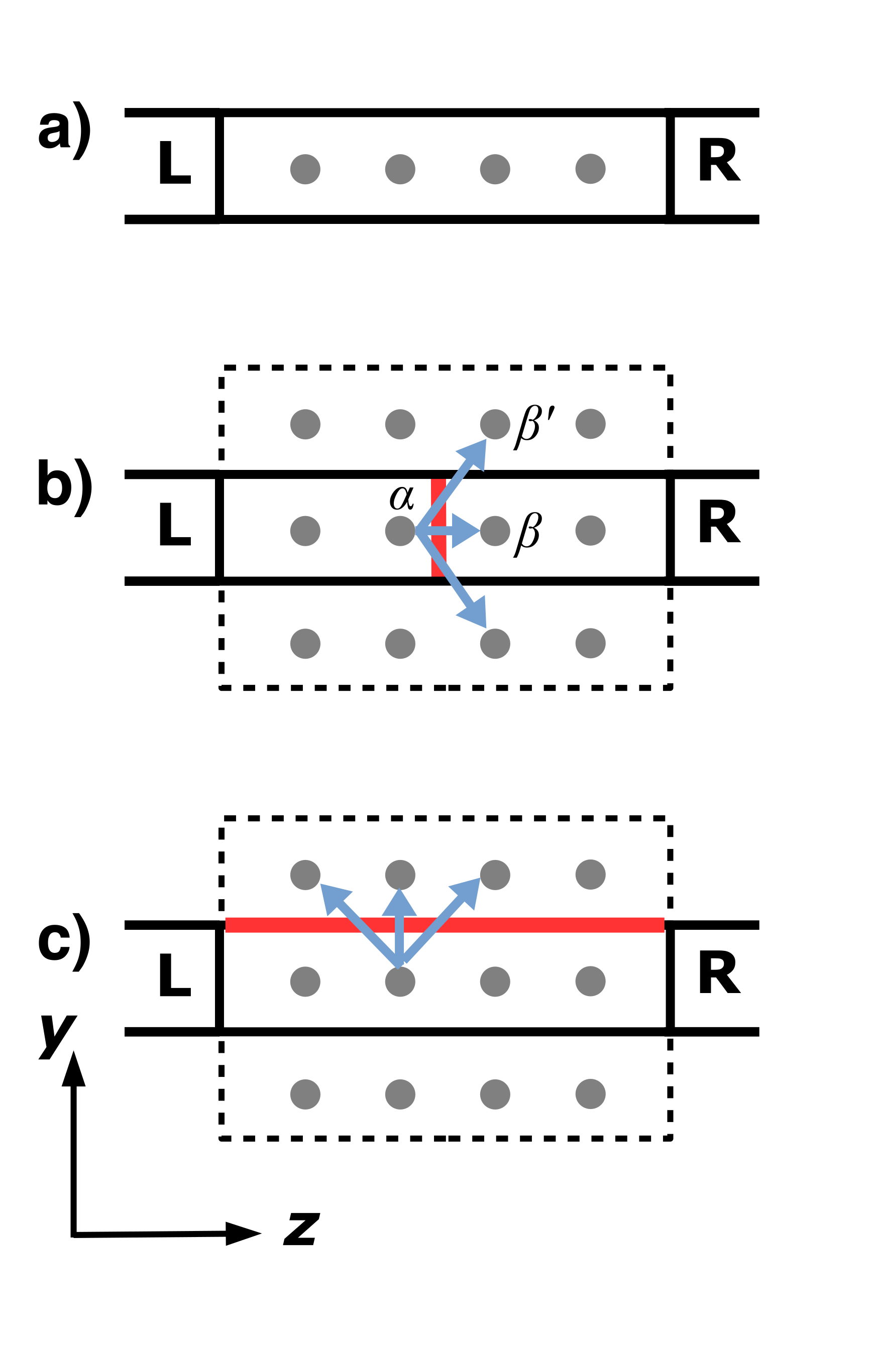
In DFT+NEGF the typical system considered is subdivided into three parts, as shown in Fig. 1: a central region of finite length , and a left-hand side (L) and a right-hand side (R) semi-infinite lead, from which electrons can flow in and out. The leads are effectively electronic baths characterized by their chemical potentials, and , and temperatures, . A bias voltage, , can be applied across the central region by displacing the leads’ chemical potentials in such a way that ( is the electron charge). The linear response limit is then achieved by taking . In order to obtain the SHE, we assume a linear drop of the potential between the electrodes. In this picture the accelerating electric field is then concentrated only inside the central region, namely over a distance , yielding a well defined steady state with a finite longitudinal charge current , where is the system’s conductance. Furthermore, as the electrons move with acceleration between the leads, the spin Hall current, , is also finite and proportional to the voltage. This means that , where is the spin Hall conductance. In the limit of large , the spin Hall current saturates to a fixed value and , where is the static SHC of an infinite crystal. This can now be calculated within a fully consistent steady state theory.
The SHC obtained by means of DFT+NEGF for ballistic systems does not necessarily have the same value as the one calculated from the Kubo formalism. This is because of the different setups and the different ways of maintaining the constant electric field. In this sense, the intrinsic SHE calculated for a ballistic system within DFT+NEGF is a distinct manifestation of the SHE. Eventually, the value of the SHC obtained within our setup should converge to the Kubo SHC in the presence of scattering and when becomes longer than the mean free path. In that case there should not be a physical difference between the two ways of setting up a steady electric field.
In the rest of this paper and, in particular, in Section IV.1, we will illustrate how these general ideas are realized in practice in calculations. Our implementation of DFT+NEGF is general and can be applied to clean and disordered systems alike. However, the focus will be only on ballistic transport, as calculations for central regions larger than the mean free path are practically too computationally demanding.
II.2 The DFT+NEGF method
We use DFT+NEGF as implemented in the Smeagol code [81, 82, 79], which is interfaced with the DFT package Siesta [83]. We employ a linear combination of numerical atomic orbitals basis set, , according to the multiple- scheme, where is a collective index spanning the quantum numbers and the atom to which a basis orbital belongs. Since the basis orbitals are non-orthogonal, their overlap integral is non-zero. In practice, we use strictly confined basis orbitals [83], namely orbitals that vanish beyond a certain cutoff radius, . Thus, the overlap integral between two orbitals will vanish, if their distance is larger than . We adopt the convention that the longitudinal charge transport direction is parallel to the Cartesian -axis, and periodic boundary conditions are applied in the transverse plane. We then indicate with the wave number in the corresponding 2-dimensional Brillouin zone. We assume that the central region is contained in a rectangular supercell. Although this is not strictly necessary, in practice it greatly simplifies the analysis of the results and the calculation of the currents for the considered materials.
Mathematically, the subdivision of a system as presented in Fig. 1 is achieved by describing the central region in terms of its KS Hamiltonian and overlap matrices, and , and by representing the leads through energy- and wave number-dependent complex self-energies . The self-energies are computed by using the algorithm of Ref. [82] and using the leads’ Hamiltonian and overlap matrices from a DFT calculation for the corresponding bulk material.
The system’s electronic and transport properties are calculated by solving the NEGF equations [67]. Specifically, we obtain the retarded Green’s function of the central region by direct inversion of the Hamiltonian with the leads’ self-energies
| (1) |
while the lesser Green’s function is defined as
| (2) |
The matrices
| (3) |
represent the strength of the electronic coupling between the left (right) lead and the central region, is the left (right) lead’s Fermi function at the chemical potential , and in Eq. (1) is a small positive real number.
The density matrix of the central region is obtained by integrating the lesser Green’s function over the energy
| (4) |
| (5) |
which is needed to compute the charge and spin currents as shown in the next section.
Since is the KS Hamiltonian, which depends itself on the charge density, Eqs. (1), (2) and (4) need to be evaluated self-consistently [81]. We note that the lead self-energies, Green’s functions and, therefore, also the (energy) density matrix depend on the bias voltage, although we have not explicitly indicated that dependence in the equations above to keep the notation short.
A system is in thermodynamic equilibrium with Fermi energy when the leads have the same chemical potential and the same temperature. Then, the effect of applying a finite bias voltage is simulated by shifting the leads relative chemical potentials, as discussed in Section II.1. This, in addition to the necessary condition of local charge neutrality, results in a relative displacement of the whole leads’ band structure. In practice, we set and . With these boundary conditions, the Hartree potential of the central region is modified to capture the voltage drop and can be evaluated self-consistently. However, in practice, for clean metals like the systems studied in this work, a self-consistent solution at finite bias can not be found as, physically, the electronic screening and the absence of scattering prevent a potential drop. We then perform self-consistent calculations only at zero-bias voltage, while finite-bias calculations are done non-self-consistently, taking the zero-bias density matrix as input, and updating it only once within the rigid shift approximation [85, 78]. As shown in Fig. 1, the shift, , applied to the leads’ chemical potentials and band structure, is bridged by a linear ramp electrostatic potential in the central region, where is the position of interface between central region and the left (right) lead. Thus, we effectively introduce an accelerating constant electric field inside the central region, and we will expect to observe a finite spin Hall current. In this paper, is carefully chosen to ensure that the calculations are performed in the linear-response limit as implied by the Landauer-Büttiker picture.
A system can also be driven out-of-equilibrium without applying any bias voltage, but by setting the leads at different temperatures, and . In that case, one first computes the lead self-energies using the Hamiltonians and overlap matrices from a DFT calculation for the corresponding bulk material with electronic temperature . Then, to obtain the density matrix, one evaluates the lesser Green’s function in Eq. (2) by entering the two different temperatures and in the Fermi functions and with the same chemical potential . The temperature difference will result in a longitudinal thermoelectric current. However, we will have no accelerating electric field across the central region. Hence, we expect no spin Hall currents. As such, comparing calculations for systems driven by a bias voltage and by a temperature difference between the leads may be useful to establish the consistency of the proposed picture for the SHE.
Since we have to include the SOC in our calculations of the SHE, the Hamiltonian of the central region assumes a non-collinear form, and it is composed of the blocks for any pair of basis orbitals with indices and . Here, and describe the spin-independent and spin-dependent parts of the Hamiltonian matrix elements, respectively. is the identity matrix, and is a vector of Pauli matrices. Similar expansions are written also for the density matrix, , and the energy density matrix, . In contrast, the overlap matrix is spin independent, that is .
An important aspect of DFT+NEGF as presented here is that, in addition to enabling the calculation of the transport properties (as shown below), it also gives access to the electronic structure of the central region. In particular, using the spin-dependent part of the density matrix, we can compute the spin density at any position in space
| (6) |
where is the number of wave numbers (i.e, points) in the transverse Brillouin zone, and is the weight associated to each of them. Such spin density is calculated in Section IV.3 showing that the SHE is accompanied by a current-induced spin dipole.
II.3 Bond currents for SHE calculations
The SHE is studied by computing the transverse spin current that emerges when a bias voltage is applied across a system, together with the associated longitudinal charge current. In order to carry out these calculations, we use the bond-current approach [76], which was first introduced for spin transport within the tight-binding formalism [74, 77] and recently extended for DFT+NEGF [79, 80]. Although the calculations presented in this paper are performed with the Smeagol code, the equations below are general and can be applied within any standard DFT+NEGF implementation.
We first compute the current between any pair of basis orbitals for a state with wave-number
| (7) |
where
| (8) |
is the charge component and
| (9) |
| (10) |
with and expressed in the same form as in Eq. (8). We note that here, both indices and refer to orbitals inside the central region supercell. However, we generally need also the bond currents that flow outside that supercell (see Fig. 2 and also appendix A in Ref. [80]). These are obtained by considering the periodic replicas of the supercell, including the appropriate Bloch phase factor in the summation
| (11) |
Here refers to an orbital in the central region, while indicates an orbital located in a periodic replica of the central region supercell, equivalent to the the orbital , from which it is separated by a translation vector .
Since we use confined basis orbitals, a bond current is zero by definition when the distance between two orbitals and is larger than the orbitals’ cutoff radii. Furthermore, since the bond currents depend on the Hamiltonian matrix elements, they have the largest values for pairs of orbitals centered at nearest neighbour and next nearest neighbour atoms, while they become negligible for pairs of distant orbitals. Thus, the number of relevant bond currents in the sum is practically limited. Once these are obtained, we can finally compute the total longitudinal charge current and the transverse spin current.
The longitudinal charge current is defined as the charge current flowing through a cross section of the scattering region perpendicular to the direction, and it is calculated as schematically illustrated in Fig. 2b. We sum the charge components of the bond currents from the orbitals on the left-hand side of the cross-section plane to the orbitals on the right hand side of it
| (12) |
Importantly, for this summation to be correctly carried out, has to run over orbitals inside the supercell central region as well as orbitals outside it and centered inside its periodic image. These two different kinds of bond currents are given respectively in Eq. (10) and Eq. (11).
The spin currents can be calculated in the same way as the charge current by performing a summation of the bond currents, but considering the spin instead of the charge components. In particular, we indicate a spin current as (, where is the index labelling the spin-polarization direction, while indicates the flow direction along one of the Cartesian axis. Importantly, from a mathematical point of view, the spin currents are components of a second-rank pseudotensor (see, for example, Ref. [80]). The structure of the spin current pseudotensor is entirely determined by the crystal symmetry. Thus, as a first validation of the calculation, one can check that the results for a material are consistent with the corresponding symmetry.
A longitudinal spin current is obtained from an equation analogous to Eq. (12) replacing and .
In contrast, a transverse spin current, that is a spin Hall current , is defined as the spin current flowing parallel to either the or the Cartesian axis and through the lateral side of the central region supercell
| (13) |
Here, and indicate the orbitals inside and outside the supercell of the central region corresponding to the scheme in Fig. 2c. Thus, is obtained from Eq. (11). We note that the spin currents have the unit of an energy. However, here we have expressed them in the same unit as the charge current by introducing the factor on the left-hand side of Eq. (9). In this way, we will be able to directly compare the relative magnitude of the longitudinal charge current and the spin Hall current.
The charge and spin conductances and can be fitted from the plot of the longitudinal charge and spin Hall currents, and , as a function of the applied bias voltage, . The obtained value at zero-temperature can then be compared to that given by the Landauer-Büttiker formula
| (14) |
where is the Planck constant and is the zero-bias transmission coefficient [86],
| (15) |
evaluated at the Fermi energy. In the linear-response limit, both Eq. (14) and the fit of the - curve must return identical results. Furthermore, must be equal to the number of transport channels in the longitudinal direction.
A bond current approach similar to ours was already employed in the scattering theory calculations of Refs. [50, 62, 66] which were mentioned in the introduction. However, we note that the implementation in those works was based on wave-functions rather than Green’s functions.
The NEGF calculations by Belashchenko et al. [75] for the SHE in Pt did not consider bond currents. The spin Hall currents were instead obtained from the “spin-orbital” torques [87]. The idea there is that a change in a local spin-orbital torque must be compensated by a variation of a local spin current, and, as a consequence, it is possible to obtain one quantity from the other. The approach by Belashchenko et al. is equivalent to ours whenever the spin currents in a material are not conserved. However, for defect-free and transversely periodic systems, like those studied here, the spin currents are instead conserved. Thus, the spin-orbital torques are zero, and therefore, the spin-Hall currents must be computed directly from the bond currents. In this regard, our approach is more general than that used in previous works, and, as shown in the following, it allows for a detailed description of the SHE.
III Computational details
DFT+NEGF calculations are performed with the local spin-density approximation (LSDA) to the exchange-correlation functional [88, 89] and the on-site approximation to the SOC [90]. This latter was generally found accurate even for materials with non-trivial spin-textures (see [91, 92, 93]). Core electrons are treated using norm-conserving Troullier-Martins pseudopotentials [94, 95] generated using the Atom code [96]. The valence electrons are expanded using the numerical atomic orbital basis set of double- plus polarization quality [97, 98]. The cutoff radii of the basis orbitals for W and Pt are obtained from Ref. [99], while those for Ta and Ir are the same as for W and Pt, respectively. In contrast, those for Au are taken from previous Smeagol calculations for molecular junctions [85]. For all materials, the pseudopotentials and basis sets have been validated to closely reproduce the electronic band structure obtained from the Quantum Espresso plane-wave code v7.0 [100].
The density matrix in Eq. (4) is calculated by splitting the integration of the lesser Green’s function into the so-called equilibrium and non-equilibrium components [81]. The equilibrium component is obtained by performing the integration along a contour in the complex energy plane [81]. We use 32 energy points along the semicircle and the imaginary line that form that contour, and we evaluate 16 poles. The non-equilibrium contribution is calculated by performing the integration over the real energy axis using at least 48 energy points within an integration range, which extends from to . Since all the studied materials are non-magnetic, we initialize the magnetic moment of each atom to be zero within double precision. This is important to accurately resolve the current-induced spin-polarization with a reduced numerical noise.
Both the zero-bias and the finite bias calculations are performed with at least a 21 21 k- point uniform grid in the transverse Brillouin zone. Using as an example the case of Pt, the convergence of the total transverse spin current with respect to the number of k-points is discussed in the Supplementary Material [101].
We consider the same material in both the leads and the central region to avoid any interface effects and, therefore, to capture bulk properties. Ta and W have bcc crystal structure, whereas Ir, Pt and Au are fcc metals. We use the experimental lattice parameters in all calculations and set the longitudinal transport direction, , along the [001] crystallographic direction. The Cartesian and axes are then oriented parallel to the [100] and [010] directions, respectively.
IV Results and Discussion
IV.1 Intrinsic SHE in Pt
We consider here fcc Pt as an example to illustrate in detail the use of DFT+NEGF to study the SHE. The calculations are performed for a system like the one schematically represented in Fig. 1. We initially consider 10 atomic layers in the central region across which we apply different voltages. The results are presented in Fig. 3.
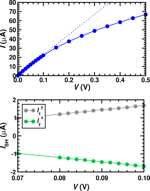
We find that the longitudinal charge current, , is accompanied by transverse spin currents with perpendicular spin polarization, and , with . These are the spin Hall currents. All the other spin currents , with and , vanish as dictated by the material’s cubic symmetry. Both the charge current and the spin Hall current are seen to vary linearly as a function of the applied bias voltage for V, which delimits the linear response regime. The charge and spin Hall conductances obtained by fitting the data to the equations and are and , respectively. The estimated is in agreement with the value obtained from the Landauer-Büttiker formula of Eq. (14), with the transmission coefficient equal to , namely the number of open transport channels at the Fermi energy. The transverse spin currents are found to vanish at zero-bias, as expected since equilibrium spin currents, albeit generally predicted in materials [102, 103], are forbidden by symmetry in fcc crystals [80]. Overall, our results show how the SHE emerges in the ballistic transport setup. Both the longitudinal charge current and spin Hall current are finite and can be obtained within the same computation.
Similar transport calculations can also be carried out by applying a temperature difference instead of the bias voltage between the leads, as described in Section II.2. On doing so, we find a finite thermoelectric longitudinal current, which depends linearly on the temperature difference. However, we observe no spin Hall currents. This negative result directly demonstrates that the emergence of the SHE requires an electric field to accelerate electrons.
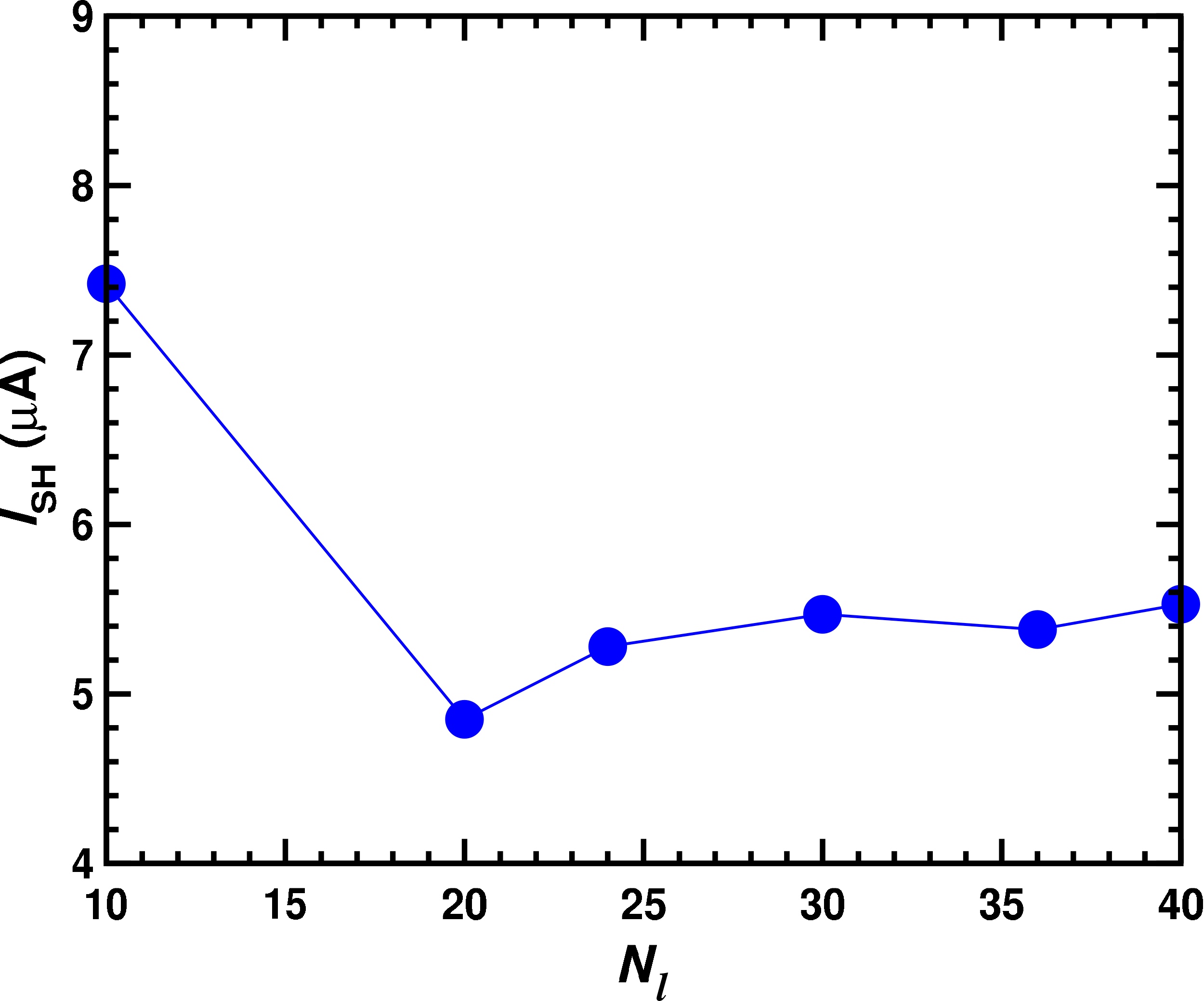
To further analyse the SHE at the quantitative level, we now increase the length of the central region from 10 atomic layers (=1.77 nm) to a maximum of 40 atomic layers (=7.65 nm). For a constant applied bias voltage, , the longitudinal charge current does not depend on the length of the central region. This is consistent with the the Landauer-Büttiker picture and further proves that our calculations are correctly performed. In contrast, the spin Hall current, , significantly varies as a function of the number of layers, , as shown in Fig. 4. The smallest value for is found for the shortest system. In the limit of long systems, when the electric field across the central region becomes infinitely small, we reach an asymptotic value , where is the lateral size of the central region. We can then estimate the SHC as argued in Section II.1. Although the maximum number of layers that one can practically consider is limited by the computational cost of the calculations, we observe in Fig. 4 that the spin Hall current has already converged for relatively small systems. Thus, from the results of the longest studied system (), we obtain that the SHC is with an error of about due to remaining numerical errors in the calculation, such as those due to the k-point sampling and the size of the lateral supercell (see Supplementary Material for a full evaluation of the error). Notably, our estimate for is within the range of the theoretical and experimental reports that one can found in literature. These go from to [30, 33, 34, 36, 48, 104, 105, 106, 107, 31, 108]. In particular, our result is in very good agreement with the SHC reported for ultra-clean samples [36].
Our computed SHC can also be compared to the value obtained from standard Kubo-formalism calculations, i.e., [31, 109], noting that our result is somewhat smaller. As discussed in Section II.1, the DFT+NEGF and the Kubo SHCs are not expected to be the same, and the different results reflect the different calculation setups and the different ways of sustaining the constant electric field. In this regard, it is interesting to note that our DFT+NEGF estimate is in quite good agreement with the value obtained via wave-function-based scattering theory calculations [48, 50], although those were performed for systems including thermal disorder within the frozen phonon approximation.
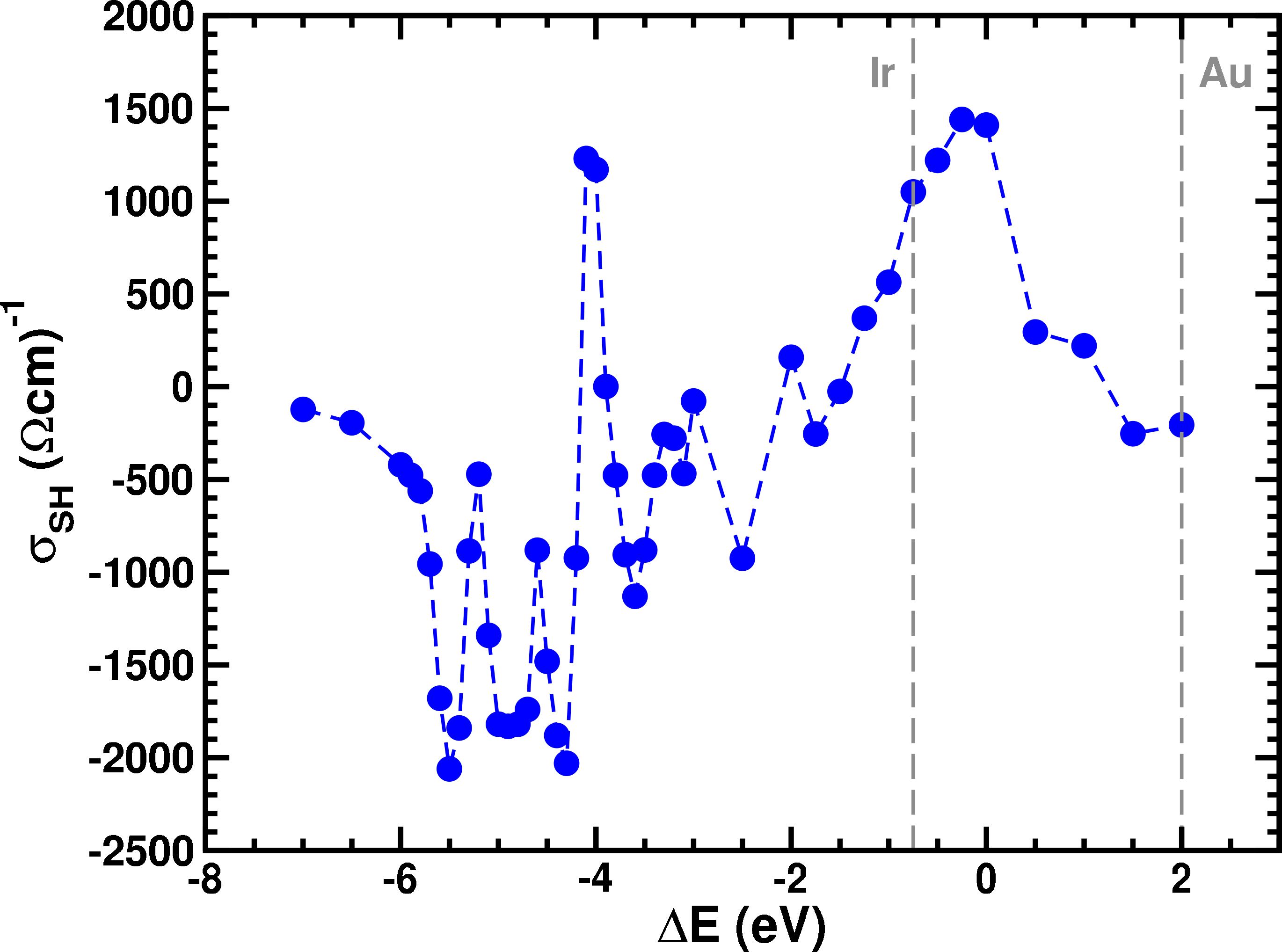
Some physical insights into the SHE can be obtained by analysing how the SHC changes as a function of the Fermi energy, or, in other words, as a function of the band filling. We can then compare the results with some generally expected trends [31]. The calculations are practically carried out non-self-consistently by applying a rigid energy shift to the true Pt Fermi energy, . The results are shown in Fig. 5. has a broad positive maximum centered at eV, namely at the Pt true Fermi energy. It then rapidly declines as increases and the Fermi energy exits the band. On the opposite end, is found to be negative for - eV, and eventually vanishes for - eV when the band becomes empty.
The SHC is generally positive (negative) when the band occupation is above (below) half-filling. This qualitative behaviour is consistent with the results from the literature [31, 30, 32] obtained with different implementations of the Kubo formalism as it reflects the underlying electronic structure of Pt. Interestingly, the broad peak centered at eV is reminiscent of the one seen in the standard plot of the energy-dependent Kubo SHC reported, for example, in Fig. 1 of Ref. [31].
A particularly interesting energy region in the plot of Fig. 5 is for between - and - eV. There, the SHC has a very strong dependence on the Fermi energy position, and we can observe sharp fluctuations, not seen in the energy-dependent Kubo SHC of Ref. [31]. This behaviour is likely related to the complex and intricate band structure around that energy region. In particular, we note a distinct feature at -4 eV, where the SHC suddenly switches from a negative to a large positive value. Regarding this point, it is useful to compare our results to the ones by Belashchenko et al. [75], who performed DFT+NEGF calculations for Pt in the presence of Anderson-like disorder. For low disorder, they observed a very similar feature to ours at -4 eV in the SHC vs plot (compare Fig. 5 with Fig. 4 in Ref. [75]). However, in their calculations, that feature disappears with increasing disorder, and they eventually recover results comparable to those from the Kubo formalism. This finding qualitatively supports the conjecture brought forward in Section II.1 that the SHC obtained by DFT+NEGF should converge to the Kubo SHC in the presence of scattering, and specifically, when the length of the central region becomes longer than the mean free path.
Finally, we can complete our analysis by also computing the SHA, , beside the SHC. In literature, the SHA is conventionally defined as the ratio of the SHC to the longitudinal charge conductivity. However, such a definition is valid for Ohmic transport, whereas here we work within the Landauer-Büttiker picture of quantum transport, and, as such, there is no notion of charge conductivity. We therefore introduce the alternative definition, , namely we define the SHA in terms of the conductance. In the case of Pt, this “ballistic SHA” is then readily obtained, and we find when is that of the longest system. The results can not be directly compared to experiments, as the ballistic conductance of Pt has never been measured. However, the ballistic SHA still serves as an intrinsic parameter uniquely relating the SHE to the material’s band structure. In the following, it will be used to compare the SHE across different metals.
IV.2 Intrinsic SHE across cubic metals
We now extend our study to the other metals with either bcc or fcc structures, where the SHE is isotropic. In all these materials, we find that the longitudinal charge current is accompanied by transverse spin currents, , like in the case of Pt. The SHC is estimated by considering central regions of different lengths and by extracting the result for the longest system, for which the spin-Hall current has converged, as explained in the previous section.
Among the fcc materials, Pt has by far the largest SHC, , which was calculated in the previous section. At the opposite extreme there is Au with a vanishing SHC equal to about 60 . Ir has a somewhat intermediate SHC, . These results are approximately the same that one would extract from Fig. 5 at the corresponding materials’ band filling, i.e., by assuming a rigid band shift of the Pt bands when going from Pt to Ir to Au, as often done in literature [30].
For the two bcc materials, Ta and W, we obtain similar intermediate absolute SHC values, but with opposite signs, and - , respectively. These values could not be inferred from Fig. 5, which describe the fcc compounds and not the bcc ones. However, the rigid band shift approximation is still valid as long as the proper bcc lattice is considered. In fact, the SHC of W can be obtained from the calculations for Ta by simply shifting the Fermi energy to artificially increase the band filling [101]. Interestingly, the result for W is quite close to the estimate from the Kubo formalism, that is [110].
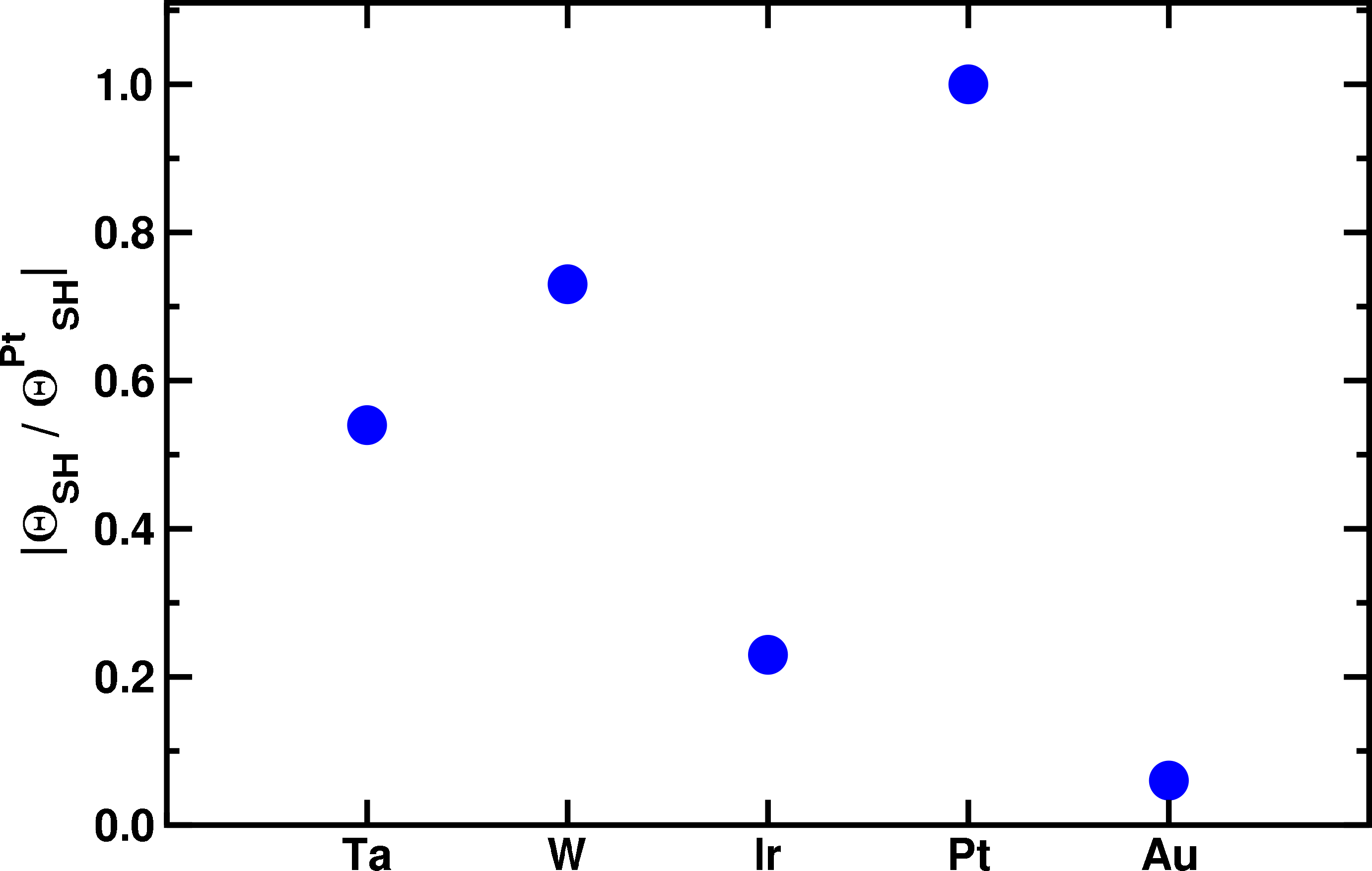
In order to compare the SHE across the various materials, we compute their SHA, , as defined in the previous section. The results, given as a fraction of the value for Pt, , are displayed in Fig. 6. We observe a rough qualitative dependence on the partial -electron count. The SHA has the largest value for Pt (), then drops for Ir () and is further enhanced for W () and Ta(). Interestingly, although the SHC of Pt is almost three times larger than that of W, the SHAs of the two materials are comparable. This is because, together with the spin conductance, the charge conductance of W also decreases and becomes equal to .
Finally, we note that W can also be found in the metastable, so-called, -phase with the A15 cubic structure. Since this system has been reported to have a large isotropic SHE [24, 19, 1, 111, 112, 113, 114, 115, 23, 116, 110], we have considered it as well. In our calculations, the SHC of -W is , which is about twice the value of bcc W and close to that of Pt. Our result therefore confirm the claims of its giant SHE.
IV.3 Current-induced spin dipole
The DFT+NEGF method allows us to obtain the electronic structure of our systems through the same calculations performed to estimate the SHC. This is a clear advantage of our approach compared to the wave-function-based implementations of scattering theory, where the details of the electronic structure of the central region are not explicitly considered. Here we analyze in particular the spin density, defined in Eq. (6).
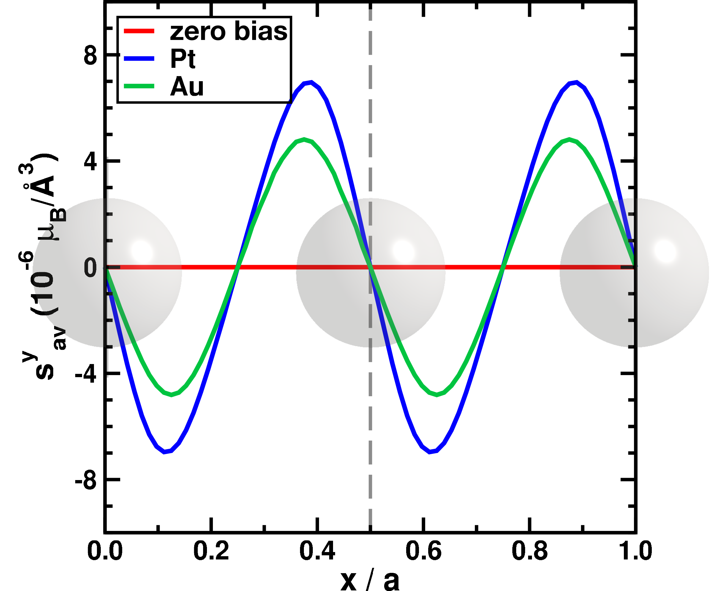
At zero bias, the spin density is zero everywhere in the central region. In contrast, at finite bias and in the presence of a longitudinal charge current, we find a position-dependent modulation of the transverse spin density components, and . In order to practically visualize this effect, we plot in Fig. 7 the so-called “spin density profile” [117, 44] in the transverse direction, namely the spin- density averaged over the plane, , with and the length and the lateral size of the cell. Similarly, we can also define the averaged spin- density , which behaves in the same way as . The results in Fig. 7 are for Pt and Au and are obtained for the same longitudinal charge current = 5.8 A.
The two materials behave in a qualitatively similar way. The spin density profile is periodic (almost sinusoidal), with a period equal to half of the cubic lattice parameter, i.e. , and integrates to zero over the unit cell. In practice, we observe the emergence of a spin dipole with the positive and negative polarities centered between the atoms. Interestingly, although the SHE of Au is almost negligible compared to that of Pt, we see in Fig. 7 that the spin dipoles for the two metals are comparable.
Mathematically, the spin dipole in a crystalline material is described by the first momentum of the spin density and has components , where is the component of the displacement vector pointing from the negative dipole polarity to the positive one, and is the unit cell volume. Since the spin density is an axial vector and the displacement is a polar vector, the spin dipole is a rank-two pseudovector, like the spin current (see Section II.3), and it has the same structure. In the non-magnetic materials considered here, the time-reversal symmetry dictates that pseudotensors vanish. Therefore, at equilibrium, no spin dipole is allowed, and all the components are zero. In contrast, when we drive a longitudinal charge current, the time-reversal symmetry is broken and, as a consequence, a spin dipole can emerge.
The phenomenon is clearly reminiscent of the ISGE, but some care is needed when making such a connection. On the one hand, in systems hosting the ISGE, a charge current induces a non-equilibrium spin density, which, when integrated over the entire volume, results in a global magnetization [118]. On the other hand, in our systems, such global magnetization is zero. The ISGE is in fact only allowed in a subset of non-centrosymmetric materials called gyrotropic [119], whereas the fcc and bcc structures are centrosymmetric. In spite of that, our calculations predict that a non-zero spin density still appears locally in the form of a spin dipole over the unit cell. In other words, we may say that the ISGE is absent as a bulk unit cell property, but is present as a local property. This situation is comparable to altermagnetism, when the breaking of the time reversal symmetry is characterized by a local spin polarization with a vanishing net spin [120]. In fact, the observed current-induced spin dipole in inversion symmetric materials can be also understood as a current-induced altermagnetism. If the inversion symmetry of one of our systems was broken making it gyrotropic, we would recover the global ISGE which could be viewed as a current-induced form of ferromagnetism.
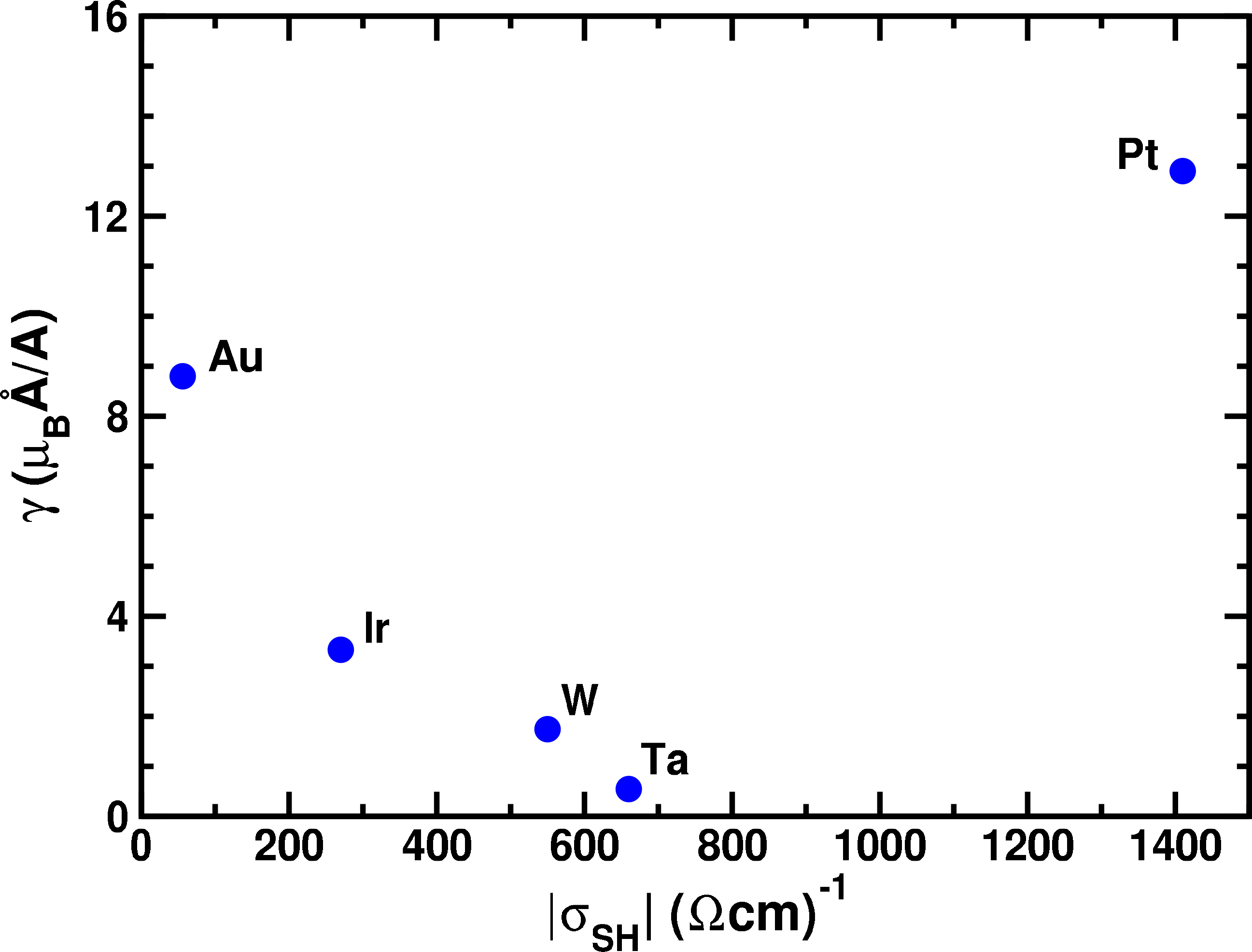
In order to perform a quantitative analysis of the current-induced spin dipole in our set-up, we find convenient to estimate the momentum of the spin density profile with the center of the dipole. Since depends linearly on the longitudinal charge current density , for small applied bias voltages, V, we define the coefficient . The calculated values of for the different materials are plotted in Fig. 8 against their SHCs. has the largest value for Au and Pt, although the two materials have extremely different SHCs, as already observed above. In contrast, is considerably smaller for W, Ta and Ir. Interestingly, when we look not only at the magnitude but also at the sign of , we find that this is opposite for W and Ta, just as the SHC computed in Section IV.2. Overall our calculation correctly reproduces the fact that the spin dipole and the spin current share the same symmetry.
A further check that the spin dipole is induced by the charge current, which breaks the time-reversal symmetry, can be carried out by applying a temperature difference, instead of a voltage bias, between the leads. In this case, we observe that the spin Hall current disappears, since electrons are not accelerated (see Section IV.1), but the spin dipole persists. Furthermore, the spin density profile appears the same for a fixed current value, independently of whether that current is driven by a bias voltage or by a temperature difference. For instance, in the case of Pt, we compute 13 A in both cases.
The current-induced spin dipole in metals was recently reported also in Ref. [44], where a different approach was employed, treating thick slabs. In that case, it is shown that the spin density profile develops sharp peaks at the surface atomic layers of the slabs, where the spatial inversion symmetry is broken, indicating the emergence of the ISGE. Those peaks decay in the interior of the slabs, where the spin density profile eventually converges to the same bulk oscillating behaviour and spin dipole seen here. Overall, for all considered materials, the results in those slabs’ interior regions are in good quantitative agreement with those calculated here for true bulk systems.
The current-induced spin dipole predicted here is probably not measurable in experiments and will not impact any performances of spintronic devices. Nonetheless, our calculations serve to illustrate the potential of our formalism. The DFT+NEGF method can be readily used to study the current-induced modulation of the spin density in real space. When applied to gyrotropic media rather than cubic materials, we expect that the approach will capture the ISGE emerging alongside the SHE, and it will therefore allow for a comparison of the two effects’ relative magnitudes.
V Summary and conclusion
In this work, we have explained how to study the SHE by means of the DFT+NEGF approach to quantum transport. The longitudinal charge and the transverse spin Hall currents are calculated through the so-called bond currents, which connect atomic orbitals along different directions. Their mathematical definition and some details for their computational implementation have been provided. The method is rather general and can be used in any electronic structure code based on a linear combination of atomic orbital basis set.
DFT+NEGF calculations have been carried out for ideal clean, namely ballistic, systems in the linear response limit. The SHE emerges when we assume a linear drop of the bias voltage potential between the two leads so that the electrons in the central region are accelerated by a uniform electric field. We then obtain a finite longitudinal charge current as well as a finite spin Hall current proportional to the applied bias voltage. In the limit of long central regions, the spin Hall current saturates to a fixed value, and we can extract the static SHC.
SHC values have been computed for the metals with fcc and bcc crystal structures. We observe that the SHC exhibits a rough dependence on the -band filling. This behavior is qualitatively consistent with previous experimental and theoretical results. The calculated absolute value of the SHC is the largest for Pt, drops for Ir, is further enhanced for W and Ta, and finally vanishes for Au, which exhibits a fully filled band.
The SHC of a material obtained by means of DFT+NEGF for ballistic systems does not necessarily have the same value as the one calculated from the standard Kubo formalism. This is because of the different computational setups and the different ways of sustaining the electric field accelerating the electrons. Yet, for some of the materials considered here, such as W, we find a fair agreement between the DFT+NEGF and Kubo results. Eventually, we expect that the value of the SHC obtained by DFT+NEGF will converge to the intrinsic Kubo SHC in the presence of scattering and when the considered central region becomes longer than the mean free path. This conjecture appears to be supported by recent DFT+NEGF calculations for Pt including large disorder [75]. Yet, our understanding of the transition between ballistic and Ohmic transport, and of the concomitant evolution of the SHC, remains very much incomplete. As such, our future studies will be dedicated towards improving our implementation of DFT+NEGF to treat larger systems and including different kinds of disorder needed to systematically link the extreme limits of ballistic and highly resistive transport.
Finally, we have shown that the DFT+NEGF approach also gives access to the current-induced modification of the spin density. This will be important to describe the ISGE and other charge-to-spin conversion phenomena. Although the ISGE is absent as a bulk global property in fcc and bcc metals because of the spatial inversion symmetry, the spin density is nonetheless modulated locally. Specifically we found that the SHE is accompanied by a spin-density dipole moment over the materials’ unit cell. We have then estimated that the amplitude of the spin-dipole of Pt and Au is larger than that of the other materials.
In conclusion, DFT+NEGF appears as a flexible approach to achieve, at the same time, an ab-initio description of the SHE and of current-induced spin density modifications in materials. Although further extensions, such as to include disorder, are required to mimic the experiments for metals, the approach presented here can be readily applied to any nano-material and device, where the transport remains completely dominated by the band structure alone [121].
Acknowledgements.
A.D. would like to thank I. Rungger and M. Stamenova for useful discussions about the bond current method. A.D. was funded by Science Foundation Ireland (SFI) and the Royal Society through the University Research Fellowship URF/R1/191769. A.B. and S.S. acknowledge the support of SFI (19/EPSRC/3605) and of the Engineering and Physical Sciences Research Council (EP/S030263/1). R.G. acknowledges the support of the European Commission FET-Open project INTERFAST (ID No. 965046). I.V.T. acknowledges support from Grupos Consolidados UPV/EHU del Gobierno Vasco (Grant No. IT1453-22) and from Grant No. PID2020-112811GB-I00 funded by MCIN/AEI/10.13039/501100011033. The computational resources were provided by the Trinity Centre for High-Performance Computing (TCHPC) and the Irish Centre for High-End Computing (ICHEC) facilities. A.B. and R.G. have contributed equally to this work.References
- Sinova et al. [2015] J. Sinova, S. O. Valenzuela, J. Wunderlich, C. H. Back, and T. Jungwirth, Spin hall effects, Rev. Mod. Phys. 87, 1213 (2015).
- Inoue and Ohno [2005] J. Inoue and H. Ohno, Taking the hall effect for a spin, Science 309, 2004 (2005).
- Kato et al. [2004] Y. K. Kato, R. C. Myers, A. C. Gossard, and D. D. Awschalom, Observation of the spin hall effect in semiconductors, Science 306, 1910 (2004).
- Sih et al. [2005] V. Sih, R. C. Myers, Y. K. Kato, W. H. Lau, A. C. Gossard, and D. D. Awschalom, Spatial imaging of the spin hall effect and current-induced polarization in two-dimensional electron gases, Nature Physics 1, 31 (2005).
- Dyakonov and Perel [1971a] M. Dyakonov and V. Perel, Current-induced spin orientation of electrons in semiconductors, Physics Letters A 35, 459 (1971a).
- Dyakonov and Perel [1971b] M. I. Dyakonov and V. Perel, Possibility of orienting electron spins with current, Soviet Journal of Experimental and Theoretical Physics Letters 13, 467 (1971b).
- Hirsch [1999] J. E. Hirsch, Spin hall effect, Phys. Rev. Lett. 83, 1834 (1999).
- Zhang [2000] S. Zhang, Spin hall effect in the presence of spin diffusion, Phys. Rev. Lett. 85, 393 (2000).
- Murakami et al. [2003] S. Murakami, N. Nagaosa, and S.-C. Zhang, Dissipationless quantum spin current at room temperature, Science 301, 1348 (2003).
- Sinova et al. [2004] J. Sinova, D. Culcer, Q. Niu, N. A. Sinitsyn, T. Jungwirth, and A. H. MacDonald, Universal intrinsic spin hall effect, Phys. Rev. Lett. 92, 126603 (2004).
- Engel et al. [2005] H.-A. Engel, B. I. Halperin, and E. I. Rashba, Theory of spin hall conductivity in -doped GaAs, Phys. Rev. Lett. 95, 166605 (2005).
- Raimondi and Schwab [2005] R. Raimondi and P. Schwab, Spin-hall effect in a disordered two-dimensional electron system, Phys. Rev. B 71, 033311 (2005).
- Dimitrova [2005] O. V. Dimitrova, Spin-hall conductivity in a two-dimensional rashba electron gas, Phys. Rev. B 71, 245327 (2005).
- Wunderlich et al. [2005] J. Wunderlich, B. Kaestner, J. Sinova, and T. Jungwirth, Experimental observation of the spin-hall effect in a two-dimensional spin-orbit coupled semiconductor system, Phys. Rev. Lett. 94, 047204 (2005).
- Stern et al. [2006] N. P. Stern, S. Ghosh, G. Xiang, M. Zhu, N. Samarth, and D. D. Awschalom, Current-induced polarization and the spin hall effect at room temperature, Phys. Rev. Lett. 97, 126603 (2006).
- Valenzuela and Tinkham [2006] S. O. Valenzuela and M. Tinkham, Direct electronic measurement of the spin hall effect, Nature 442, 176 (2006).
- Jungwirth et al. [2012] T. Jungwirth, J. Wunderlich, and K. Olejník, Spin hall effect devices, Nature Materials 11, 382 (2012).
- Wang et al. [2013] K. L. Wang, J. G. Alzate, and P. K. Amiri, Low-power non-volatile spintronic memory: STT-RAM and beyond, Journal of Physics D: Applied Physics 46, 074003 (2013).
- Hoffmann [2013] A. Hoffmann, Spin hall effects in metals, IEEE Transactions on Magnetics 49, 5172 (2013).
- Kimura et al. [2007] T. Kimura, Y. Otani, T. Sato, S. Takahashi, and S. Maekawa, Room-temperature reversible spin hall effect, Phys. Rev. Lett. 98, 156601 (2007).
- Vila et al. [2007] L. Vila, T. Kimura, and Y. Otani, Evolution of the spin hall effect in Pt nanowires: Size and temperature effects, Phys. Rev. Lett. 99, 226604 (2007).
- Liu et al. [2011] L. Liu, T. Moriyama, D. C. Ralph, and R. A. Buhrman, Spin-torque ferromagnetic resonance induced by the spin hall effect, Phys. Rev. Lett. 106, 036601 (2011).
- Liu et al. [2012] L. Liu, C.-F. Pai, Y. Li, H. W. Tseng, D. C. Ralph, and R. A. Buhrman, Spin-torque switching with the giant spin hall effect of Tantalum, Science 336, 555 (2012).
- Pai et al. [2012] C.-F. Pai, L. Liu, Y. Li, H. W. Tseng, D. C. Ralph, and R. A. Buhrman, Spin transfer torque devices utilizing the giant spin Hall effect of tungsten, Applied Physics Letters 101, 122404 (2012).
- Nakayama et al. [2013] H. Nakayama, M. Althammer, Y.-T. Chen, K. Uchida, Y. Kajiwara, D. Kikuchi, T. Ohtani, S. Geprägs, M. Opel, S. Takahashi, R. Gross, G. E. W. Bauer, S. T. B. Goennenwein, and E. Saitoh, Spin hall magnetoresistance induced by a nonequilibrium proximity effect, Phys. Rev. Lett. 110, 206601 (2013).
- Wang et al. [2014] H. L. Wang, C. H. Du, Y. Pu, R. Adur, P. C. Hammel, and F. Y. Yang, Scaling of spin hall angle in 3d, 4d, and 5d metals from /metal spin pumping, Phys. Rev. Lett. 112, 197201 (2014).
- Li et al. [2020] X. Li, S.-J. Lin, M. Dc, Y.-C. Liao, C. Yao, A. Naeemi, W. Tsai, and S. X. Wang, Materials requirements of high-speed and low-power spin-orbit-torque magnetic random-access memory, IEEE Journal of the Electron Devices Society 8, 674 (2020).
- Zhu et al. [2021] L. Zhu, D. C. Ralph, and R. A. Buhrman, Maximizing spin-orbit torque generated by the spin Hall effect of Pt, Applied Physics Reviews 8, 031308 (2021).
- Mosendz et al. [2010] O. Mosendz, J. E. Pearson, F. Y. Fradin, G. E. W. Bauer, S. D. Bader, and A. Hoffmann, Quantifying spin hall angles from spin pumping: Experiments and theory, Phys. Rev. Lett. 104, 046601 (2010).
- Tanaka et al. [2008] T. Tanaka, H. Kontani, M. Naito, T. Naito, D. S. Hirashima, K. Yamada, and J. Inoue, Intrinsic spin hall effect and orbital hall effect in and transition metals, Phys. Rev. B 77, 165117 (2008).
- Guo et al. [2008] G. Y. Guo, S. Murakami, T.-W. Chen, and N. Nagaosa, Intrinsic spin hall effect in Platinum: First-principles calculations, Phys. Rev. Lett. 100, 096401 (2008).
- Morota et al. [2011] M. Morota, Y. Niimi, K. Ohnishi, D. H. Wei, T. Tanaka, H. Kontani, T. Kimura, and Y. Otani, Indication of intrinsic spin hall effect in and transition metals, Phys. Rev. B 83, 174405 (2011).
- Isasa et al. [2015a] M. Isasa, E. Villamor, L. E. Hueso, M. Gradhand, and F. Casanova, Temperature dependence of spin diffusion length and spin hall angle in Au and Pt, Phys. Rev. B 91, 024402 (2015a).
- Isasa et al. [2015b] M. Isasa, E. Villamor, L. E. Hueso, M. Gradhand, and F. Casanova, Erratum: Temperature dependence of spin diffusion length and spin hall angle in Au and Pt, Phys. Rev. B 92, 019905 (2015b).
- Zhu et al. [2019] L. Zhu, L. Zhu, M. Sui, D. C. Ralph, and R. A. Buhrman, Variation of the giant intrinsic spin hall conductivity of Pt with carrier lifetime, Science Advances 5, eaav8025 (2019).
- Sagasta et al. [2016] E. Sagasta, Y. Omori, M. Isasa, M. Gradhand, L. E. Hueso, Y. Niimi, Y. Otani, and F. Casanova, Tuning the spin hall effect of Pt from the moderately dirty to the superclean regime, Phys. Rev. B 94, 060412 (2016).
- Otani et al. [2017] Y. Otani, M. Shiraishi, A. Oiwa, E. Saitoh, and S. Murakami, Spin conversion on the nanoscale, Nature Physics 13, 829 (2017).
- Ganichev et al. [2019] S. D. Ganichev, M. Trushin, and J. Schliemann, Spin polarisation by current, in Spintronics Handbook, Second Edition, edited by E. Y. Tsymbal and I. Žutić (CRC Press Taylor & Francis Group, 2019).
- Edelstein [1990] V. Edelstein, Spin polarization of conduction electrons induced by electric current in two-dimensional asymmetric electron systems, Solid State Communications 73, 233 (1990).
- Allen et al. [2015] G. Allen, S. Manipatruni, D. E. Nikonov, M. Doczy, and I. A. Young, Experimental demonstration of the coexistence of spin hall and rashba effects in bilayers, Phys. Rev. B 91, 144412 (2015).
- Du et al. [2020] Y. Du, H. Gamou, S. Takahashi, S. Karube, M. Kohda, and J. Nitta, Disentanglement of spin-orbit torques in / bilayers with the presence of spin hall effect and rashba-edelstein effect, Phys. Rev. Applied 13, 054014 (2020).
- Shen et al. [2021] J. Shen, Z. Feng, P. Xu, D. Hou, Y. Gao, and X. Jin, Spin-to-charge conversion in bilayer revisited, Phys. Rev. Lett. 126, 197201 (2021).
- Yue et al. [2018] D. Yue, W. Lin, J. Li, X. Jin, and C. L. Chien, Spin-to-charge conversion in bi films and bilayers, Phys. Rev. Lett. 121, 037201 (2018).
- Droghetti and Tokatly [2023] A. Droghetti and I. V. Tokatly, Current-induced spin polarization at metallic surfaces from first principles, Phys. Rev. B 107, 174433 (2023).
- Lowitzer et al. [2011] S. Lowitzer, M. Gradhand, D. Ködderitzsch, D. V. Fedorov, I. Mertig, and H. Ebert, Extrinsic and intrinsic contributions to the spin hall effect of alloys, Phys. Rev. Lett. 106, 056601 (2011).
- Fedorov et al. [2013] D. V. Fedorov, C. Herschbach, A. Johansson, S. Ostanin, I. Mertig, M. Gradhand, K. Chadova, D. Ködderitzsch, and H. Ebert, Analysis of the giant spin hall effect in Cu(Bi) alloys, Phys. Rev. B 88, 085116 (2013).
- Chadova et al. [2015] K. Chadova, D. V. Fedorov, C. Herschbach, M. Gradhand, I. Mertig, D. Ködderitzsch, and H. Ebert, Separation of the individual contributions to the spin hall effect in dilute alloys within the first-principles Kubo-Středa approach, Phys. Rev. B 92, 045120 (2015).
- Wang et al. [2016] L. Wang, R. J. H. Wesselink, Y. Liu, Z. Yuan, K. Xia, and P. J. Kelly, Giant room temperature interface spin hall and inverse spin hall effects, Phys. Rev. Lett. 116, 196602 (2016).
- Hönemann et al. [2019] A. Hönemann, C. Herschbach, D. V. Fedorov, M. Gradhand, and I. Mertig, Spin and charge currents induced by the spin hall and anomalous hall effects upon crossing ferromagnetic/nonmagnetic interfaces, Phys. Rev. B 99, 024420 (2019).
- Nair et al. [2021a] R. S. Nair, M. S. Rang, and P. J. Kelly, Spin hall effect in a thin Pt film, Phys. Rev. B 104, L220411 (2021a).
- Kohn [1999] W. Kohn, Nobel lecture: Electronic structure of matter—wave functions and density functionals, Rev. Mod. Phys. 71, 1253 (1999).
- Yao and Fang [2005] Y. Yao and Z. Fang, Sign changes of intrinsic spin hall effect in semiconductors and simple metals: First-principles calculations, Phys. Rev. Lett. 95, 156601 (2005).
- Guo [2009] G. Y. Guo, Ab initio calculation of intrinsic spin Hall conductivity of Pd and Au, Journal of Applied Physics 105, 07C701 (2009).
- Gradhand et al. [2012] M. Gradhand, D. V. Fedorov, F. Pientka, P. Zahn, I. Mertig, and B. L. Györffy, First-principle calculations of the Berry curvature of Bloch states for charge and spin transport of electrons, Journal of Physics: Condensed Matter 24, 213202 (2012).
- Ködderitzsch et al. [2015] D. Ködderitzsch, K. Chadova, and H. Ebert, Linear response Kubo-Bastin formalism with application to the anomalous and spin hall effects: A first-principles approach, Phys. Rev. B 92, 184415 (2015).
- Ryoo et al. [2019] J. H. Ryoo, C.-H. Park, and I. Souza, Computation of intrinsic spin hall conductivities from first principles using maximally localized wannier functions, Phys. Rev. B 99, 235113 (2019).
- Zhang et al. [2021] Y. Zhang, Q. Xu, K. Koepernik, R. Rezaev, O. Janson, J. Železný, T. Jungwirth, C. Felser, J. van den Brink, and Y. Sun, Different types of spin currents in the comprehensive materials database of nonmagnetic spin hall effect, npj Computational Materials 7, 167 (2021).
- Sanvito [2005] S. Sanvito, Ab-initio methods for spin-transport at the nanoscale level, in Handbook of Computational Nanotechnology, Vol. 5, edited by M. Rieth and W. Schommers (American Scientific Publishers, 2005).
- Landauer [1957] R. Landauer, Spatial variation of currents and fields due to localized scatterers in metallic conduction, IBM Journal of Research and Development 1, 223 (1957).
- Büttiker [1986] M. Büttiker, Four-terminal phase-coherent conductance, Phys. Rev. Lett. 57, 1761 (1986).
- Buttiker [1988] M. Buttiker, Symmetry of electrical conduction, IBM Journal of Research and Development 32, 317 (1988).
- Wesselink et al. [2019] R. J. H. Wesselink, K. Gupta, Z. Yuan, and P. J. Kelly, Calculating spin transport properties from first principles: Spin currents, Phys. Rev. B 99, 144409 (2019).
- Khomyakov et al. [2005] P. A. Khomyakov, G. Brocks, V. Karpan, M. Zwierzycki, and P. J. Kelly, Conductance calculations for quantum wires and interfaces: Mode matching and green’s functions, Phys. Rev. B 72, 035450 (2005).
- Xia et al. [2006] K. Xia, M. Zwierzycki, M. Talanana, P. J. Kelly, and G. E. W. Bauer, First-principles scattering matrices for spin transport, Phys. Rev. B 73, 064420 (2006).
- Liu et al. [2015] Y. Liu, Z. Yuan, R. J. H. Wesselink, A. A. Starikov, M. van Schilfgaarde, and P. J. Kelly, Direct method for calculating temperature-dependent transport properties, Phys. Rev. B 91, 220405 (2015).
- Nair et al. [2021b] R. S. Nair, E. Barati, K. Gupta, Z. Yuan, and P. J. Kelly, Spin-flip diffusion length in transition metal elements: A first-principles benchmark, Phys. Rev. Lett. 126, 196601 (2021b).
- Datta [1995] S. Datta, Electronic Transport in Mesoscopic Systems (Cambridge University Press, Cambridge, UK, 1995).
- Brandbyge et al. [2002] M. Brandbyge, J.-L. Mozos, P. Ordejón, J. Taylor, and K. Stokbro, Density-functional method for nonequilibrium electron transport, Phys. Rev. B 65, 165401 (2002).
- Taylor et al. [2001] J. Taylor, H. Guo, and J. Wang, Ab initio modeling of quantum transport properties of molecular electronic devices, Phys. Rev. B 63, 245407 (2001).
- Chioncel et al. [2015] L. Chioncel, C. Morari, A. Östlin, W. H. Appelt, A. Droghetti, M. M. Radonjić, I. Rungger, L. Vitos, U. Eckern, and A. V. Postnikov, Transmission through correlated heterostructures, Phys. Rev. B 92, 054431 (2015).
- Droghetti et al. [2022a] A. Droghetti, M. M. Radonjić, L. Chioncel, and I. Rungger, Dynamical mean-field theory for spin-dependent electron transport in spin-valve devices, Phys. Rev. B 106, 075156 (2022a).
- Nikolić et al. [2005a] B. K. Nikolić, L. P. Zârbo, and S. Souma, Mesoscopic spin hall effect in multiprobe ballistic spin-orbit-coupled semiconductor bridges, Phys. Rev. B 72, 075361 (2005a).
- Nikolić et al. [2005b] B. K. Nikolić, S. Souma, L. P. Zârbo, and J. Sinova, Nonequilibrium spin hall accumulation in ballistic semiconductor nanostructures, Phys. Rev. Lett. 95, 046601 (2005b).
- Nikolić et al. [2006] B. K. Nikolić, L. P. Zârbo, and S. Souma, Imaging mesoscopic spin hall flow: Spatial distribution of local spin currents and spin densities in and out of multiterminal spin-orbit coupled semiconductor nanostructures, Phys. Rev. B 73, 075303 (2006).
- [75] K. Belashchenko, G. Baez Flores, W. Fang, A. Kovalev, M. van Schilfgaarde, P. Haney, and M. Stiles, Breakdown of the drift-diffusion model for transverse spin transport in a disordered Pt film, arXiv:2309.00183v1 .
- Todorov [2002] T. N. Todorov, Tight-binding simulation of current-carrying nanostructures, Journal of Physics: Condensed Matter 14, 3049 (2002).
- Theodonis et al. [2006] I. Theodonis, N. Kioussis, A. Kalitsov, M. Chshiev, and W. H. Butler, Anomalous bias dependence of spin torque in magnetic tunnel junctions, Phys. Rev. Lett. 97, 237205 (2006).
- Xie et al. [2016] Y. Xie, I. Rungger, K. Munira, M. Stamenova, S. Sanvito, and A. W. Ghosh, Spin transfer torque: A multiscale picture, in Nanomagnetic and Spintronic Devices for Energy‐Efficient Memory and Computing, edited by J. Atulasimha and S. Bandyopadhyay (John Wiley & Sons, Ltd, 2016).
- Rungger et al. [2020] I. Rungger, A. Droghetti, and M. Stamenova, Non-equilibrium green’s function methods for spin transport and dynamics, in Handbook of Materials Modeling: Methods: Theory and Modeling, edited by W. Andreoni and S. Yip (Springer International Publishing, Cham, 2020).
- Droghetti et al. [2022b] A. Droghetti, I. Rungger, A. Rubio, and I. V. Tokatly, Spin-orbit induced equilibrium spin currents in materials, Phys. Rev. B 105, 024409 (2022b).
- Rocha et al. [2006] A. R. Rocha, V. M. García-Suárez, S. Bailey, C. Lambert, J. Ferrer, and S. Sanvito, Spin and molecular electronics in atomically generated orbital landscapes, Phys. Rev. B 73, 085414 (2006).
- Rungger and Sanvito [2008] I. Rungger and S. Sanvito, Algorithm for the construction of self-energies for electronic transport calculations based on singularity elimination and singular value decomposition, Phys. Rev. B 78, 035407 (2008).
- Soler et al. [2002] J. M. Soler, E. Artacho, J. D. Gale, A. García, J. Junquera, P. Ordejón, and D. Sánchez-Portal, The SIESTA method for ab initio order-n materials simulation, Journal of Physics: Condensed Matter 14, 2745 (2002).
- Zhang et al. [2011] R. Zhang, I. Rungger, S. Sanvito, and S. Hou, Current-induced energy barrier suppression for electromigration from first principles, Phys. Rev. B 84, 085445 (2011).
- Rudnev et al. [2017] A. V. Rudnev, V. Kaliginedi, A. Droghetti, H. Ozawa, A. Kuzume, M.-A. Haga, P. Broekmann, and I. Rungger, Stable anchoring chemistry for room temperature charge transport through graphite-molecule contacts, Science Advances 3, e1602297 (2017).
- Datta [2005] S. Datta, Quantum Transport: Atom to Transistor (Cambridge University Press, Cambridge, 2005).
- Belashchenko et al. [2019] K. D. Belashchenko, A. A. Kovalev, and M. van Schilfgaarde, First-principles calculation of spin-orbit torque in a Co/Pt bilayer, Phys. Rev. Mater. 3, 011401 (2019).
- von Barth and Hedin [1972] U. von Barth and L. Hedin, A local exchange-correlation potential for the spin polarized case. i, Journal of Physics C: Solid State Physics 5, 1629 (1972).
- Vosko et al. [1980] S. H. Vosko, L. Wilk, and M. Nusair, Accurate spin-dependent electron liquid correlation energies for local spin density calculations: a critical analysis, Canadian Journal of Physics 58, 1200 (1980).
- Fernández-Seivane et al. [2006] L. Fernández-Seivane, M. A. Oliveira, S. Sanvito, and J. Ferrer, On-site approximation for spin–orbit coupling in linear combination of atomic orbitals density functional methods, Journal of Physics: Condensed Matter 18, 7999 (2006).
- Jakobs et al. [2015] S. Jakobs, A. Narayan, B. Stadtmüller, A. Droghetti, I. Rungger, Y. S. Hor, S. Klyatskaya, D. Jungkenn, J. Stöckl, M. Laux, O. L. A. Monti, M. Aeschlimann, R. J. Cava, M. Ruben, S. Mathias, S. Sanvito, and M. Cinchetti, Controlling the spin texture of topological insulators by rational design of organic molecules, Nano Letters 15, 6022 (2015).
- Narayan et al. [2012] A. Narayan, I. Rungger, and S. Sanvito, Topological surface states scattering in antimony, Phys. Rev. B 86, 201402 (2012).
- Narayan et al. [2014] A. Narayan, I. Rungger, A. Droghetti, and S. Sanvito, Ab initio transport across bismuth selenide surface barriers, Phys. Rev. B 90, 205431 (2014).
- Troullier and Martins [1991a] N. Troullier and J. L. Martins, Efficient pseudopotentials for plane-wave calculations, Phys. Rev. B 43, 1993 (1991a).
- Troullier and Martins [1991b] N. Troullier and J. L. Martins, Efficient pseudopotentials for plane-wave calculations. II. Operators for fast iterative diagonalization, Phys. Rev. B 43, 8861 (1991b).
- [96] S. Froyen, N. Troullier, J. L. Martins, and A. García, ATOM code for the generation of norm-conserving pseudopotentials, https://docs.siesta-project.org/projects/atom/en/latest/index.html, Accessed: 2022-07-15.
- Artacho et al. [1999] E. Artacho, D. Sánchez-Portal, P. Ordejón, A. García, and J. M. Soler, Linear-scaling ab-initio calculations for large and complex systems, physica status solidi (b) 215, 809 (1999).
- Junquera et al. [2001] J. Junquera, Ó. Paz, D. Sánchez-Portal, and E. Artacho, Numerical atomic orbitals for linear-scaling calculations, Physical Review B 64, 235111 (2001).
- Rivero et al. [2015] P. Rivero, V. M. García-Suárez, D. Pereñiguez, K. Utt, Y. Yang, L. Bellaiche, K. Park, J. Ferrer, and S. Barraza-Lopez, Systematic pseudopotentials from reference eigenvalue sets for dft calculations, Computational Materials Science 98, 372 (2015).
- Giannozzi et al. [2009] P. Giannozzi, S. Baroni, N. Bonini, M. Calandra, R. Car, C. Cavazzoni, D. Ceresoli, G. L. Chiarotti, M. Cococcioni, I. Dabo, A. D. Corso, S. de Gironcoli, S. Fabris, G. Fratesi, R. Gebauer, U. Gerstmann, C. Gougoussis, A. Kokalj, M. Lazzeri, L. Martin-Samos, N. Marzari, F. Mauri, R. Mazzarello, S. Paolini, A. Pasquarello, L. Paulatto, C. Sbraccia, S. Scandolo, G. Sclauzero, A. P. Seitsonen, A. Smogunov, P. Umari, and R. M. Wentzcovitch, QUANTUM ESPRESSO: a modular and open-source software project for quantum simulations of materials, Journal of Physics: Condensed Matter 21, 395502 (2009).
- [101] See supplemental material at [URL will be inserted by publisher] for convergence of global spin currents with k-point grid, variation in computed spin-hall conductivity with lateral cell size and k-point grid and comparison between Landauer-formalism-derived and bond-current-derived conductances.
- Rashba [2003] E. I. Rashba, Spin currents in thermodynamic equilibrium: The challenge of discerning transport currents, Phys. Rev. B 68, 241315 (2003).
- Tokatly [2008] I. V. Tokatly, Equilibrium spin currents: Non-abelian gauge invariance and color diamagnetism in condensed matter, Phys. Rev. Lett. 101, 106601 (2008).
- Nguyen et al. [2016] M.-H. Nguyen, D. C. Ralph, and R. A. Buhrman, Spin torque study of the spin hall conductivity and spin diffusion length in platinum thin films with varying resistivity, Phys. Rev. Lett. 116, 126601 (2016).
- Obstbaum et al. [2016] M. Obstbaum, M. Decker, A. K. Greitner, M. Haertinger, T. N. G. Meier, M. Kronseder, K. Chadova, S. Wimmer, D. Ködderitzsch, H. Ebert, and C. H. Back, Tuning spin hall angles by alloying, Phys. Rev. Lett. 117, 167204 (2016).
- Zhang et al. [2015] W. Zhang, M. B. Jungfleisch, W. Jiang, Y. Liu, J. E. Pearson, S. G. E. t. Velthuis, A. Hoffmann, F. Freimuth, and Y. Mokrousov, Reduced spin-hall effects from magnetic proximity, Phys. Rev. B 91, 115316 (2015).
- Stamm et al. [2017] C. Stamm, C. Murer, M. Berritta, J. Feng, M. Gabureac, P. M. Oppeneer, and P. Gambardella, Magneto-optical detection of the spin hall effect in Pt and W thin films, Phys. Rev. Lett. 119, 087203 (2017).
- Dai et al. [2019] Y. Dai, S. J. Xu, S. W. Chen, X. L. Fan, D. Z. Yang, D. S. Xue, D. S. Song, J. Zhu, S. M. Zhou, and X. Qiu, Observation of giant interfacial spin hall angle in /pt heterostructures, Phys. Rev. B 100, 064404 (2019).
- Nardelli et al. [2018] M. B. Nardelli, F. T. Cerasoli, M. Costa, S. Curtarolo, R. De Gennaro, M. Fornari, L. Liyanage, A. R. Supka, and H. Wang, PAOFLOW: A utility to construct and operate on ab initio hamiltonians from the projections of electronic wavefunctions on atomic orbital bases, including characterization of topological materials, Computational Materials Science 143, 462 (2018).
- McHugh et al. [2020] O. L. W. McHugh, W. F. Goh, M. Gradhand, and D. A. Stewart, Impact of impurities on the spin hall conductivity in -W, Phys. Rev. Mater. 4, 094404 (2020).
- Hao et al. [2015] Q. Hao, W. Chen, and G. Xiao, Beta () tungsten thin films: Structure, electron transport, and giant spin Hall effect, Applied Physics Letters 106, 182403 (2015).
- Hao and Xiao [2015] Q. Hao and G. Xiao, Giant spin hall effect and switching induced by spin-transfer torque in a structure with perpendicular magnetic anisotropy, Phys. Rev. Appl. 3, 034009 (2015).
- Qu et al. [2014] D. Qu, S. Y. Huang, B. F. Miao, S. X. Huang, and C. L. Chien, Self-consistent determination of spin hall angles in selected metals by thermal spin injection, Phys. Rev. B 89, 140407 (2014).
- Karnad et al. [2018] G. V. Karnad, C. Gorini, K. Lee, T. Schulz, R. Lo Conte, A. W. J. Wells, D.-S. Han, K. Shahbazi, J.-S. Kim, T. A. Moore, H. J. M. Swagten, U. Eckern, R. Raimondi, and M. Kläui, Evidence for phonon skew scattering in the spin hall effect of platinum, Phys. Rev. B 97, 100405 (2018).
- Qu et al. [2018] D. Qu, S. Y. Huang, G. Y. Guo, and C. L. Chien, Inverse spin hall effect in alloy films, Phys. Rev. B 97, 024402 (2018).
- Hahn et al. [2013] C. Hahn, G. de Loubens, O. Klein, M. Viret, V. V. Naletov, and J. Ben Youssef, Comparative measurements of inverse spin hall effects and magnetoresistance in YIG/Pt and YIG/Ta, Phys. Rev. B 87, 174417 (2013).
- Tokatly et al. [2015] I. V. Tokatly, E. E. Krasovskii, and G. Vignale, Current-induced spin polarization at the surface of metallic films: A theorem and an ab initio calculation, Phys. Rev. B 91, 035403 (2015).
- Calavalle et al. [2022] F. Calavalle, M. Suárez-Rodríguez, B. Martín-García, A. Johansson, D. C. Vaz, H. Yang, I. V. Maznichenko, S. Ostanin, A. Mateo-Alonso, A. Chuvilin, I. Mertig, M. Gobbi, F. Casanova, and L. E. Hueso, Gate-tuneable and chirality-dependent charge-to-spin conversion in tellurium nanowires, Nature Materials 21, 526 (2022).
- Tenzin et al. [2023] K. Tenzin, A. Roy, H. Jafari, B. Banas, F. T. Cerasoli, M. Date, A. Jayaraj, M. Buongiorno Nardelli, and J. Sławińska, Analogs of rashba-edelstein effect from density functional theory, Phys. Rev. B 107, 165140 (2023).
- Šmejkal et al. [2022] L. Šmejkal, J. Sinova, and T. Jungwirth, Emerging research landscape of altermagnetism, Phys. Rev. X 12, 040501 (2022).
- Rao et al. [2023] Q. Rao, W.-H. Kang, H. Xue, Z. Ye, X. Feng, K. Watanabe, T. Taniguchi, N. Wang, M.-H. Liu, and D.-K. Ki, Ballistic transport spectroscopy of spin-orbit-coupled bands in monolayer graphene on WSe2 (2023), arXiv:2303.01018 [cond-mat.mes-hall] .