Evidence for -shifted Cooper quartets in PbTe nanowire three-terminal Josephson junctions
Abstract
Josephson junctions are typically characterized by a single phase difference across two superconductors. This conventional two-terminal Josephson junction can be generalized to a multi-terminal device where the Josephson energy contains terms that result from entanglement of multiple independent phase variables. It was recently proposed that such multi-terminal couplings should result in a -shifted quartet supercurrent. We show for the first time experimental signature of this -shifted supercurrent, by using a three-terminal Josephson junction based on selective-area-grown PbTe nanowires. We further observe conductance steps at zero magnetic field co-existent with supercurrent in both two- and three-terminal devices, indicating ballistic superconductivity in the few quantum modes regime. Superconducting transport in the few-modes regime is a necessary condition for realizing topologically protected bound states such as Majorana zero modes in one-dimensional nanowires and Weyl nodes in multi-terminal Josephson junctions.
Introduction
Conventional Josephson junctions are two-terminal devices characterized by a single phase difference Josephson1962 . In general, Josephson energy of a junction with -terminals contains independent phase differences. It was recently theorized that a -supercurrent contribution should be present in multi-terminal Josephson junctions resulting from the quartet supercurrent due to multi-terminal couplings Freyn2011 ; Melin2023 ; Melin2023_3tjj ; melin2023magnetointerferometry ; Jonckheere2023 . Andreev bound state spectra of such multi-terminal Josephson junctions (MTJJs) can realize topologically protected Weyl nodes in dimensional phase space spectrum Riwar2016 ; Meyer2017 ; Xie2017 ; Xie2018 ; Xie2022 . Realization of these phenomena require multiple superconducting electrodes to be phase-coherently coupled by a single scattering region. Furthermore, observation of Weyl nodes requires the number of conductance modes to be close to unity Riwar2016 ; Meyer2017 ; Eriksson2017 .
Previous attempts to build these devices have utilized two-dimensional electron gases such as graphene or III-V semiconductors (e.g. InAs) Draelos2018 ; Cohen2018 ; Pankratova2020 ; Gino2020 ; arnault2021multiterminal ; graziano2022 ; Arnault2022 ; Huang2022 ; Gupta2023 . In these devices the two-terminal couplings are much stronger compared than the multi-terminal coupling. This results in devices behaving as a classical network of two-terminal Josephson junctions and hence unlikely to realize a multi-terminal band structure or -shifted quartet currents.
In this work, we utilize selective-area-grown (SAG) PbTe nanowires Fabrizio_Bakkers2022 to make Josephson devices. These SAG nanowires can be grown crystalline along multiple crystallographic directions Fabrizio_Bakkers2022 . This allows for construction of MTJJs where the natural quantum confinement accommodated by the wire cross-section allows for coherent coupling of multiple superconducting electrodes by a single scattering region. We observe signatures of the recently proposed -shifted supercurrent in the diffraction pattern, in the form of an enhanced critical current for small magnetic fields bulaevskii1978 ; weides2006 ; frolov2006 ; Kang2022 , along with characteristic differential resistance maps in the space of bias currents.
Semiconducting (SM) nanowires coupled with superconductors (SC) also hold potential to realize Majorana zero modes (MZMs) Doh2005 ; Lutchyn2010 ; Oreg2010 ; Lutchyn2018 ; Laroche2019 , which may have applications in fault tolerant quantum computing Kitaev2003 ; Nayak2008 ; Sarma2015 . For more than a decade, hybrid materials systems consisting of III-V semiconductors (e.g. InAs, InSb etc.), coupled with superconductors (e.g. Al, Sn, Nb etc.) have been the single most studied experimental platform in the search for MZMs Mourik2012 ; deng2012anomalous ; albrecht2016exponential ; gul2018ballistic ; vaitiekenas2020flux . However, no clear evidence of MZMs has been seen in these material systems kayyalha2020absence ; Yu2021 ; valentini2021nontopological ; jiang2023zerobias ; frolov2023smoking . One of the leading challenges toward the realization of MZMs with III-V semiconductors has been disorder Liu2012 ; Pan2021 ; Pan2021_2 ; Ahn2021 ; Mourik2012 . Recently, PbTe semiconducting nanowires have gained attention as an alternative material platform to realize MZMs with the expectation that the large dielectric constant of PbTe ( in bulk) may help screen disorder Huang2021 ; Cao2022 . PbTe nanowires have the other necessary ingredients for realizing MZMs such as large g-factors and spin-orbit interaction Fabrizio_Bakkers_gfactor_2022 ; Fabrizio_Bakkers2022 ; Gomanko2022 . Large mobilities and ballistic transport have been shown in thin film PbTe structures Allgaier1958 ; SPRINGHOLZ1993302 ; grabecki2007quantum . Recently, quantum point contacts Song2023 ; Wang2023 and induced superconductivity HaoZhang2023_SC ; li2023selectiveareagrown have been demonstrated in PbTe nanowires. However, demonstration of clean ballistic transport coexistent with induced superconductivity is lacking in PbTe nanowires. In our work, we observe quantized conductance plateaus co-existent with supercurrent in both two- and three-terminal devices indicating ballistic superconductivity in the regime of few quantum modes. These results establish PbTe SAG as a promising material system for the exploration of Majorana and MTJJ topological states that addresses major challenges of other platforms through simultaneous disorder mitigation, geometrical confinement and as-grown, potentially scalable, desired geometries.
Results
Device Architecture

The devices are fabricated on SAG PbTe (see Supplementary Information Section I) nanowires. We use superconducting Al contacts to induce superconductivity and metal electrodes are used to enable electrostatic gating of the scattering region, resulting in the structure shown in Figure 1a. Scanning electron microscope images (SEM) of two and three terminal Josephson junctions along with measurement schematics is shown in Figure 1b and c respectively. Two-terminal devices are measured in the voltage-bias configuration and three-terminal devices are measured in the current-bias configuration. The spacing between superconducting electrodes is measured to be nm for two terminal devices and nm for three-terminal devices. We present four devices in this work, labeled Device . We begin by discussing results of induced superconductivity in two-terminal devices (Device 1,2 and 3), demonstrating ballistic superconductivity. We then focus on results from our three-terminal device (Device 4) and discuss magnetic field diffraction pattern and differential resistance maps as a function of two bias currents, and .
Induced Superconductivity and Ballistic Transport

To characterize induced superconductivity, DC measurements are performed in a dilution refrigerator at the base temperature of mK. An out-of-plane magnetic field, , is applied using a superconducting magnet. The source-drain terminals of Device 1 are biased using a DC voltage source () and the DC source-drain current () is measured. We first set the gate voltage to a value V. Upon subtraction of series resistance (), that includes resistance of the low-pass filters, the transimpedance amplifier and a small contact resistance, device resistance is obtained as a function of and (Figure 2a). The magnetic field diffraction pattern is consistent with one-dimensional supercurrent flow with only one central diffraction lobe. We also observe Fiske resonances coon1965josephson above the zero resistance region in the central lobe indicating a well-defined Josephson cavity. A similar diffraction pattern is observed as a function of in-plane magnetic field (Supplementary Information Figure 2a), further confirming the one-dimensional nature of supercurrent flow. We have also measured Josephson junctions with different wire diameters with minimum diameter of nm (see Supplementary Information Figure 2b, c), demonstrating high yield of Josephson devices. All the measured devices showed induced superconductivity. Tuning to negative values reduces the switching current () and increases normal state resistance, showing induced gate tunable superconductivity in PbTe (Figure 2b). Somewhat large electric fields (corresponding to ) are required to observe an appreciable change in the critical current of the device. This we believe could be due to unintentional higher levels of Pb in some of the nanowires during growth.

From the same material growth batch there are devices (e.g. Device 2) on which complete pinch-off of the channel is observed; these may have lower levels of Pb. Figure 2c shows a map of device resistance () as function of and for Device 2. When the device is in superconducting state, voltage drop across the device is zero, resulting in . Critical current contours are thus observed as areas of zero resistance for small bias along with conductance plateaus at higher bias values as a function of (Figure 2d). The step height of these plateaus differs from the conductance quantum , and the quantization weakens for higher values of conductance. This is likely due to the effect of finite source-drain bias on the conductance. At finite bias, the value of the conductance steps is determined by the number of quasi-1D subbands falling within the bias window set by Kouwenhoven1989 ; Patel1991 ; Gallagher2014 ; Lee2019 . It is not possible to do zero bias conductance measurements on a Josephson device as the device is superconducting at . The presence of quantized normal state resistance along with supercurrent demonstrates ballistic Josephson junctions. Similar results were reproduced between two pairs of a three-terminal Josephson device. This is one of the necessary conditions for the realization of Weyl nodes in MTJJs.
To further characterize the ballistic few-mode transport in Device 2 we apply a 2.8 T out-of-plane magnetic field to drive the device from the superconducting to normal state and again perform DC measurements as a function of and . The resulting data, plotted in Figure 3a, show diamond-shaped regions of approximately uniform conductance. We note that we are now plotting bias voltage as , which reflects only the portion of the applied source-drain voltage that is actually dropped along the device. This subtraction results in the pronounced taper observed in Figure 3a,c, and allows us to directly relate the height of the conductance diamonds to the subband spacing in the device’s quasi-1D band structureKouwenhoven1989 ; Patel1991 . Linecuts of this data, shown in Figure 3b, show that these conductance plateaus align with multiples of 0.5 at low bias, consistent with Zeeman-split subbands. This further strengthens the signatures of ballisticity seen at zero-field.
In order to conclusively demonstrate quantization conductance at zero magnetic field in our SAG PbTe wires, we measure Device 3, which consists of a 200 nm gate-defined channel and uses Ti/Au contacts (see Supplementary Information section III for the device image), eliminating any complicating superconducting features at low bias. We characterize the conductance of this device as a function of and . As in Device 2, we observe diamonds of uniform conductance in the gate vs. bias map, shown in Figure 3c. Linecuts in bias, shown in Figure 3d, confirm these to be the 1.0, 2.0, and 3.0 quantized conductance plateaus, corresponding to the first three spin-degenerate subbands. This zero-field conductance quantization is consistent with recent results published on PbTe SAG wires grown on CdTe Song2023 ; Wang2023 . Zero-field quantized conductance, as seen in Devices 2 and 3, is a necessary milestone towards realizing MZMs in nanowires, as the transition to topological superconductivity requires few-mode ballistic transport and fields of only a few hundreds of mT Mourik2012 ; Lutchyn2010 ; Oreg2010 . Additionally, zero-field quantized conductance is qualitatively suggestive of low levels of device disordervanWeperen2013 , the importance of which has been stressed in recent theoretical studies of MZMs in realistic devicesPan2021 ; Pan2021_2 ; Lutchyn2010 . Further details of quantized conductance in Device 3 are presented in Supplementary Information section III.
In Figure 2 and Figure 3 several checkerboard like resonances are superimposed on the conductance data. These are consistent with an accidental gate-tunable quantum dot present in these nanowires Gomanko2022 . We resolve such quantum dot features in Device 2 by exploring the zero conductance region (Supplementary Information section IV). We find results consistent with previous characterizations of quantum dots on PbTe, such as near-zero charging energy and large anisotropic g-factors Gomanko2022 ; Fabrizio_Bakkers2022 .
Three-terminal Josephson junctions
Having demonstrated that clean ballistic transport along with superconductivity can be realized in this material system, we now turn our attention to the three-terminal Josephson junctions. We control two bias currents, and , and measure two voltages, and , to construct differential resistance maps as shown in Figure 4a for Device 4. We observe three superconducting arms in the differential resistance maps along with a central superconducting feature. The superconducting arms are roughly along , and (see Supplementary Information Figure V for the full dataset). In the central superconducting region, at , superconductivity is split into two distinct pockets at finite value of separated by regions of finite resistance. Importantly, note that at and we observe a finite differential resistance. Such rich structure in the central superconducting feature has not been observed in previous MTJJ experiments. In the presence of -supercurrent, the critical current can be zero at bulaevskii1978 ; weides2006 ; frolov2006 ; Kang2022 . This suggests the presence of -supercurrent in our device due to multi-terminal coherent processes taking place in the central region of the device Freyn2011 ; Melin2023 ; Melin2023_3tjj ; melin2023magnetointerferometry ; Jonckheere2023 .
To further clarify this point, we performed magnetic field measurements at fixed values of , sweeping and varying the out-of-plane magnetic field, . The resulting interference patterns on these devices show a non-convex pattern, as can be seen in Figure 4 b in the transition from the superconducting state to the normal state. At , another resonance with finite differential resistance is present that appears to taper to near . Such non-convex diffraction patterns in two-terminal devices have been interpreted as a signature of the Josephson current-phase relation (CR) bulaevskii1978 ; weides2006 ; frolov2006 ; Kang2022 . This is the first clear experimental detection of the recently proposed -shifted quartet transport in MTJJs Freyn2011 ; Melin2023 ; Melin2023_3tjj ; melin2023magnetointerferometry ; Jonckheere2023 . Previous experimental evidence of quartet transport Cohen2018 ; Huang2022 is in the non-equilibrium regime at finite voltages, however some of the differential resistance map signature can be due to the correlated phase dynamics in the circuit model and may not necessarily be due to quartets Arnault2022 . However, to our knowledge there are no theoretical models that can explain the -shifted supercurrent in a multi-terminal Josephson junctions, other than multi-terminal couplings.
To understand the transport properties of the differential resistance map and supercurrent, we model our device’s Josephson energy including terms corresponding to both two-terminal and three-terminal processes as shown in Equation 1. Terms containing only two-phase variables result from two-terminal processes that can be understood in terms of the semiclassical RCSJ network model, as discussed in Refs. Gino2020 ; graziano2022 . The superconducting arms appear when a single Josephson junction present between any pair of terminals is superconducting. The slopes of these superconducting arms in the - plane can be understood by the resistor network model presented in Refs. Gino2020 ; graziano2022 ; Gupta2023 .
| (1) |
However, the central superconducting feature and the non-convex interference pattern cannot be captured by this standard RCSJ network model. In order to fit the observed interference pattern we derive expression for critical current as a function of magnetic field by starting from the expression for the total Josephson energy of the device as shown in Equation 1. This includes contribution from the two-terminal process with energy and three-terminal process with energy , the -shifted current phase relation sets Melin2023 .
Gauge invariance allows us to remove one of the phases while magnetic field sets the phase difference . Upon maximizing for critical current in the free phase variable we get the following expression for the critical current (See Supplementary Information section VI for the derivation) for small magnetic fields and small :
| (2) |
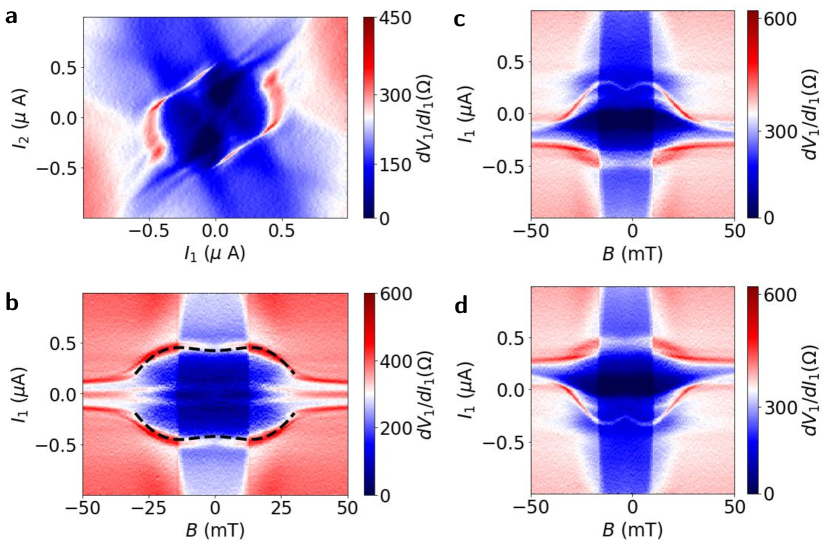
We fit Equation 2 (A, A) to the non-convex resonance present at A in our experimental data and obtain the curve as shown in Figure 4b by a dashed black line. This agreement between our experiment and theory serves as compelling evidence for the presence of phase-coherent three-terminal processes, also known as quartet transport. The quartets correspond to Cooper pair entanglement across the three superconducting terminals. The inner resonance near can be fitted with the same ratio of . We can further control this supercurrent by application of . For positive (negative) value of , the non-convex diffraction pattern appears only for the positive (negative) value of and remains flat for negative (positive) values of (Figure 4c,d). The center of interference pattern is also shifted on the axis. This shift is simply a consequence of current conservation. However, the non-reciprocal -supercurrent (superconducting diode effect) is not accounted for by current conservation. This injected current in terminal-2 may serve as another source for tuning the phase differences. Our current model does not account for these processes and hence we have not fitted any theoretical curve to these datasets.
Discussion
In summary, we have shown zero-field conductance quantization along with the presence of superconductivity in multiple devices. Such reproducible observation of clean transport demonstrates the strong potential that PbTe SAG nanowires hold for MZMs and topological MTJJ devices. We expect that further improvement in material growth can allow for even better coupling of superconductors and may further improve transport properties.
We show reproducible -shifted quartet currents in three-terminal Josephson junctions, demonstrating evidence for phase-coherent multi-terminal couplings. Along with this we show quantized between different pairs of the terminals in a three-terminal device, necessary for the observation of Weyl nodes in the Andreev bound state spectra. Correlated phase dynamics Arnault2022 are not expected to produce the observed supercurrent. We have measured the temperature dependence of the supercurrent as shown in Supplementary Information Figure VII. Furthermore, we do not observe such non-convex diffraction pattern on any of the measured two-terminal devices, hence this effect is unlikely to be due to any of the underlying material properties, but rather stems from the multi-terminal geometry. Addition of superconducting loops, split-gates and more terminals can allow for custom tuning of the supercurrent. MTJJs allow for creation of junctions without any magnetic elements in the junction area. Such junctions may find applications in compact superconducting supercomputing and superconducting memories Ortlepp2007 ; Tomohiro_KAMIYA2018 .
Methods
Device Fabrication
Standard electron beam lithography (EBL) and ion-mill etch techniques were used to fabricate the superconducting Ti/Al ( nm) contacts. Approximately 40 nm of dielectric was deposited using thermal atomic layer deposition (ALD). Using EBL, gates are defined over the junction area and electrodes are deposited using electron-beam evaporation of Ti/Au (5 nm/80 nm).
Measurement Details
Resistance data on Device-1 and Device 2, differential resistance maps on Device 4, and conductance quantization data on Device 2 were obtained by low-noise DC transport measurements in a 3He/4He dilution refrigerator. For the conductance quantization data on Device 3 standard low-frequency lock-in techniques were used with a small excitation voltage and a frequency of 19 Hz. For all measurements on the two-terminal devices the raw data is corrected by subtracting the series filter and the ammeter resistances which combine to give 9.8 k. Low-pass Gaussian filtering was used to smooth numerical derivatives.
Data and Code Availability
Source data for the figures presented in this paper and the data plotting code is available from authors upon request.
References
- (1) Josephson, B. Possible new effects in superconductive tunnelling. Phys. Lett. 1, 251–253 (1962).
- (2) Freyn, A., Douçot, B., Feinberg, D. & Mélin, R. Production of nonlocal quartets and phase-sensitive entanglement in a superconducting beam splitter. Phys. Rev. Lett. 106, 257005 (2011).
- (3) Mélin, R., Danneau, R. & Winkelmann, C. B. Proposal for detecting the -shifted cooper quartet supercurrent. Phys. Rev. Res. 5, 033124 (2023).
- (4) Mélin, R. & Feinberg, D. Quantum interferometer for quartets in superconducting three-terminal josephson junctions. Phys. Rev. B 107, L161405 (2023).
- (5) Mélin, R., Winkelmann, C. B. & Danneau, R. Magneto-interferometry of multiterminal josephson junctions (2023). eprint 2311.12964.
- (6) Jonckheere, T. et al. Quartet currents in a biased three-terminal diffusive josephson junction. Phys. Rev. B 108, 214517 (2023).
- (7) Riwar, R. P., Houzet, M., Meyer, J. S. & Nazarov, Y. V. Multi-terminal Josephson junctions as topological matter. Nat. Commun. 7, 11167 (2016).
- (8) J. S. Meyer & Houzet, M. Nontrivial Chern Numbers in Three-Terminal Josephson Junctions. Phys. Rev. Lett. 119, 136807 (2017).
- (9) Xie, H. Y., Vavilov, M. G. & Levchenko, A. Topological Andreev bands in three-terminal Josephson junctions. Phys. Rev. B 96, 161406(R) (2017).
- (10) Xie, H. Y., Vavilov, M. G. & Levchenko, A. Weyl nodes in Andreev spectra of multiterminal Josephson junctions: Chern numbers, conductances, and supercurrents. Phys. Rev. B 97, 035443 (2018).
- (11) Xie, H.-Y., Hasan, J. & Levchenko, A. Non-abelian monopoles in the multiterminal josephson effect. Phys. Rev. B 105, L241404 (2022).
- (12) Eriksson, E., Riwar, R.-P., Houzet, M., Meyer, J. S. & Nazarov, Y. V. Topological transconductance quantization in a four-terminal josephson junction. Phys. Rev. B 95, 075417 (2017).
- (13) Draelos, A. W. et al. Supercurrent Flow in Multiterminal Graphene Josephson Junctions. Nano Lett. 19, 1039–1043 (2019).
- (14) Cohen, Y. et al. Nonlocal supercurrent of quartets in a three-terminal Josephson junction. Proc. Natl. Acad. Sci. U.S.A. 115, 6991–6994 (2018).
- (15) Pankratova, N. et al. Multiterminal josephson effect. Phys. Rev. X 10, 031051 (2020).
- (16) Graziano, G. V., Lee, J. S., Pendharkar, M., Palmstrøm, C. J. & Pribiag, V. S. Transport studies in a gate-tunable three-terminal josephson junction. Phys. Rev. B 101, 054510 (2020).
- (17) Arnault, E. G. et al. Multiterminal inverse ac josephson effect. Nano Letters 21, 9668–9674 (2021).
- (18) Graziano, G. V. et al. Selective control of conductance modes in multi-terminal josephson junctions. Nature Communications 2022 13:1 13, 1–8 (2022).
- (19) Arnault, E. G. et al. Dynamical stabilization of multiplet supercurrents in multiterminal josephson junctions. Nano Letters 22, 7073–7079 (2022). PMID: 35997531.
- (20) Huang, K.-F. et al. Evidence for 4e charge of cooper quartets in a biased multi-terminal graphene-based josephson junction. Nature Communications 13, 3032 (2022).
- (21) Gupta, M. et al. Gate-tunable superconducting diode effect in a three-terminal josephson device. Nature Communications 2023 14:1 14, 1–8 (2023).
- (22) Jung, J. et al. Selective area growth of pbte nanowire networks on inp. Advanced Functional Materials 32, 2208974 (2022).
- (23) Bulaevskii, L., Kuzii, V. & Sobyanin, A. On possibility of the spontaneous magnetic flux in a josephson junction containing magnetic impurities. Solid State Communications 25, 1053–1057 (1978).
- (24) Weides, M. et al. 0- josephson tunnel junctions with ferromagnetic barrier. Physical review letters 97, 247001 (2006).
- (25) Frolov, S., Van Harlingen, D., Bolginov, V., Oboznov, V. & Ryazanov, V. Josephson interferometry and shapiro step measurements of superconductor-ferromagnet-superconductor 0- junctions. Physical Review B 74, 020503 (2006).
- (26) Kang, K. et al. van der waals josephson junctions. Nano Letters 22, 5510–5515 (2022).
- (27) Doh, Y.-J. et al. Tunable supercurrent through semiconductor nanowires. Science 309, 272–5 (2005).
- (28) Lutchyn, R. M., Sau, J. D. & Das Sarma, S. Majorana fermions and a topological phase transition in semiconductor-superconductor heterostructures. Phys. Rev. Lett. 105, 077001 (2010).
- (29) Oreg, Y., Refael, G. & von Oppen, F. Helical liquids and majorana bound states in quantum wires. Phys. Rev. Lett. 105, 177002 (2010).
- (30) Lutchyn, R. M. et al. Majorana zero modes in superconductor-semiconductor heterostructures. Nat. Rev. Mater. 3, 52–68 (2018).
- (31) Laroche, D. et al. Observation of the 4-periodic Josephson effect in indium arsenide nanowires. Nat. Commun. 10, 245 (2019).
- (32) Kitaev, A. Y. Fault-tolerant quantum computation by anyons. Ann. Phys. (N.Y.) 303, 2–30 (2003).
- (33) Nayak, C., Simon, S. H., Stern, A., Freedman, M. & Das Sarma, S. Non-Abelian anyons and topological quantum computation. Rev. Mod. Phys. 80, 1083–1159 (2008).
- (34) Sarma, S. D., Freedman, M. & Nayak, C. Majorana zero modes and topological quantum computation. npj Quantum Inf. 1, 15001 (2015).
- (35) Mourik, V. et al. Signatures of majorana fermions in hybrid superconductor-semiconductor nanowire devices. Science 336, 1003–1007 (2012).
- (36) Deng, M. et al. Anomalous zero-bias conductance peak in a nb–insb nanowire–nb hybrid device. Nano letters 12, 6414–6419 (2012).
- (37) Albrecht, S. M. et al. Exponential protection of zero modes in majorana islands. Nature 531, 206–209 (2016).
- (38) Gül, Ö. et al. Ballistic majorana nanowire devices. Nature nanotechnology 13, 192–197 (2018).
- (39) Vaitiekėnas, S. et al. Flux-induced topological superconductivity in full-shell nanowires. Science 367, eaav3392 (2020).
- (40) Kayyalha, M. et al. Absence of evidence for chiral majorana modes in quantum anomalous hall-superconductor devices. Science 367, 64–67 (2020).
- (41) Yu, P. et al. Non-majorana states yield nearly quantized conductance in proximatized nanowires. Nature Physics 17, 482–488 (2021).
- (42) Valentini, M. et al. Nontopological zero-bias peaks in full-shell nanowires induced by flux-tunable andreev states. Science 373, 82–88 (2021).
- (43) Jiang, Y. et al. Zero-bias conductance peaks at zero applied magnetic field due to stray fields from integrated micromagnets in hybrid nanowire quantum dots (2023). eprint 2305.19970.
- (44) Frolov, S. M. et al. ”smoking gun” signatures of topological milestones in trivial materials by measurement fine-tuning and data postselection (2023). eprint 2309.09368.
- (45) Liu, J., Potter, A. C., Law, K. T. & Lee, P. A. Zero-bias peaks in the tunneling conductance of spin-orbit-coupled superconducting wires with and without majorana end-states. Phys. Rev. Lett. 109, 267002 (2012).
- (46) Das Sarma, S. & Pan, H. Disorder-induced zero-bias peaks in majorana nanowires. Phys. Rev. B 103, 195158 (2021).
- (47) Pan, H., Liu, C.-X., Wimmer, M. & Das Sarma, S. Quantized and unquantized zero-bias tunneling conductance peaks in majorana nanowires: Conductance below and above . Phys. Rev. B 103, 214502 (2021).
- (48) Ahn, S., Pan, H., Woods, B., Stanescu, T. D. & Das Sarma, S. Estimating disorder and its adverse effects in semiconductor majorana nanowires. Phys. Rev. Mater. 5, 124602 (2021).
- (49) Huang, Y. & Shklovskii, B. I. Disorder effects in topological insulator nanowires. Phys. Rev. B 104, 054205 (2021).
- (50) Cao, Z. et al. Numerical study of pbte-pb hybrid nanowires for engineering majorana zero modes. Phys. Rev. B 105, 085424 (2022).
- (51) ten Kate, S. C. et al. Small charging energies and g-factor anisotropy in pbte quantum dots. Nano Letters 22, 7049–7056 (2022). PMID: 35998346, eprint https://doi.org/10.1021/acs.nanolett.2c01943.
- (52) Gomanko, M. et al. Spin and Orbital Spectroscopy in the Absence of Coulomb Blockade in Lead Telluride Nanowire Quantum Dots. SciPost Phys. 13, 089 (2022).
- (53) Allgaier, R. S. & Scanlon, W. W. Mobility of electrons and holes in pbs, pbse, and pbte between room temperature and 4.2°k. Phys. Rev. 111, 1029–1037 (1958).
- (54) Springholz, G., Bauer, G. & Ihninger, G. Mbe of high mobility pbte films and pbte/pb1-xeuxte heterostructures. Journal of Crystal Growth 127, 302–307 (1993).
- (55) Grabecki, G. Quantum ballistic phenomena in nanostructures of paraelectric pbte. Journal of applied physics 101 (2007).
- (56) Song, W. et al. Conductance quantization in pbte nanowires. Phys. Rev. B 108, 045426 (2023).
- (57) Wang, Y. et al. Ballistic pbte nanowire devices. Nano Letters 23, 11137–11144 (2023). PMID: 37948302.
- (58) Zhang, Z. et al. Proximity effect in pbte-pb hybrid nanowire josephson junctions. Phys. Rev. Mater. 7, 086201 (2023).
- (59) Li, R. et al. Selective-area-grown pbte-pb planar josephson junctions for quantum devices (2023). eprint 2311.16815.
- (60) Coon, D. & Fiske, M. D. Josephson ac and step structure in the supercurrent tunneling characteristic. Physical Review 138, A744 (1965).
- (61) Kouwenhoven, L. P. et al. Nonlinear conductance of quantum point contacts. Phys. Rev. B 39, 8040–8043 (1989).
- (62) Patel, N. K. et al. Evolution of half plateaus as a function of electric field in a ballistic quasi-one-dimensional constriction. Phys. Rev. B 44, 13549–13555 (1991).
- (63) Gallagher, P., Lee, M., Williams, J. R. & Goldhaber-Gordon, D. Gate-tunable superconducting weak link and quantum point contact spectroscopy on a strontium titanate surface. Nature Physics 10, 748–752 (2014).
- (64) Lee, J. S. et al. Transport Studies of Epi-Al/InAs Two-Dimensional Electron Gas Systems for Required Building-Blocks in Topological Superconductor Networks. Nano Lett. 19, 3083 (2019).
- (65) van Weperen, I., Plissard, S. R., Bakkers, E. P. A. M., Frolov, S. M. & Kouwenhoven, L. P. Quantized conductance in an insb nanowire. Nano Letters 13, 387–391 (2013). PMID: 23259576.
- (66) Ortlepp, T. et al. Rsfq circuitry using intrinsic -phase shifts. IEEE Transactions on Applied Superconductivity 17, 659–663 (2007).
- (67) Kamiya, T., Tanaka, M., Sano, K. & Fujimaki, A. Energy/space-efficient rapid single-flux-quantum circuits by using -shifted josephson junctions. IEICE Transactions on Electronics E101.C, 385–390 (2018).
Acknowledgements
All aspects of the work at UMN were supported by the Department of Energy under Award No. DE-SC0019274. Portions of this work were conducted in the Minnesota Nano Center, which is supported by the National Science Foundation through the National Nano Coordinated Infrastructure Network (NNCI) under Award Number ECCS-1542202. Eindhoven University of Technology acknowledges the research program “Materials for the Quantum Age” (QuMat) for financial support. This program (registration number 024.005.006) is part of the Gravitation program financed by the Dutch Ministry of Education, Culture and Science (OCW). Eindhoven University of Technology acknowledges European Research Council (ERC TOCINA 834290).
Author Contributions
M.G. and V.S.P. designed the experiments. M.G. and V.K. fabricated the devices. M.G. performed the measurements on Device 1, 2 and 4 and analysed the data. G.M. and L.S. fabricated Device 3. C.R. performed measurements and analyzed data on Device 3. P.L. and E.P.A.M.B. provided the nanowires. R.M. provided the theoretical model for the three-terminal device. All authors contributed to writing the manuscript. V.S.P. supervised the project.
Competing interests
The authors declare no competing interests.