Reconfigurable Frequency Multipliers Based on Complementary Ferroelectric Transistors
Abstract
Frequency multipliers, a class of essential electronic components, play a pivotal role in contemporary signal processing and communication systems. They serve as crucial building blocks for generating high-frequency signals by multiplying the frequency of an input signal. However, traditional frequency multipliers that rely on nonlinear devices often require energy- and area-consuming filtering and amplification circuits, and emerging designs based on an ambipolar ferroelectric transistor require costly non-trivial characteristic tuning or complex technology process. In this paper, we show that a pair of standard ferroelectric field effect transistors (FeFETs) can be used to build compact frequency multipliers without aforementioned technology issues. By leveraging the tunable parabolic shape of the 2FeFET structures’ transfer characteristics, we propose four reconfigurable frequency multipliers, which can switch between signal transmission and frequency doubling. Furthermore, based on the 2FeFET structures, we propose four frequency multipliers that realize triple, quadruple frequency modes, elucidating a scalable methodology to generate more multiplication harmonics of the input frequency. Performance metrics such as maximum operating frequency, power, etc., are evaluated and compared with existing works. We also implement a practical case of frequency modulation scheme based on the proposed reconfigurable multipliers without additional devices. Our work provides a novel path of scalable and reconfigurable frequency multiplier designs based on devices that have characteristics similar to FeFETs, and show that FeFETs are a promising candidate for signal processing and communication systems in terms of maximum operating frequency and power.
I Introduction
The demand for higher frequency signals in modern electronics has necessitated the development of innovative techniques for frequency generation [1, 2, 3, 4, 5]. Frequency multipliers, a fundamental category of electronic circuits, have emerged as indispensable tools in this endeavor [6]. A frequency multiplier produces an output signal with a frequency that is an integer multiple of the input frequency. Most of this fundamental operation is achieved through nonlinear signal processing techniques, wherein the input signal is subjected to a series of transformations to generate a higher frequency output[7].
The currently widely used nonlinear devices include two types: Schottky diodes and metal oxide field effect transistors (MOSFETs). Schottky diodes are utilized as nonlinear elements in the frequency multipliers, which perform exceptionally well at high frequencies. However, the structural characteristics of Schottky diodes pose challenges when integrating them with other components like amplifiers and oscillators. Additionally, Schottky diode based multipliers require significant input driving power to ensure sufficient conversion gains due to the inherent passivity of diodes [8, 9, 10]. Alternatively, MOSFET based multipliers are compatible with CMOS technology, and can leverage the transconductance characteristics of transistors to amplify voltage fluctuations at input and/or output, thereby enhancing the conversion gain even with low input power [11, 12, 13, 14, 15, 16, 17]. However, such nonlinear devices not only generate the desired frequency signal but also produce extra harmonics, thus necessitating complex filtering circuits, which are often energy- and area-consuming [9, 17, 16]. To date, more efficient frequency multiplication techniques are still undergoing.
Recently, innovative approaches harnessing the ambipolar parabolic characteristic curve of ferroelectric field effect transistors (FeFETs) to induce second harmonic were introduced [18, 19, 20]. Through the controlled programming of ambipolar FeFETs, the developed single-transistor frequency multipliers that can switch between signal transmission and frequency doubling have been demonstrated, exhibiting low power and compact area. However, it is worth noting that these frequency multiplier are limited to operating at approximately 1 MHz/10 kHz and achieving only first and second harmonic generation, which cannot meet the high-frequency requirements of communication systems. Furthermore, they suffer from either the non-trivial tuning that ensures the symmetrical ambipolarity, or costly and complex nanowire tunneling FET technology. More general reconfigurable frequency multiplier design with scalable and efficient harmonic generations are highly desired.
In this paper, we propose a general and economic design methodology for building compact and reconfigurable frequency multipliers with scalable harmonic generation capability. Taking the complementary FeFETs as representative devices, we show how to build four 2FeFET structures (i.e., 2 n-type FeFETs (nFeFETs), 2 p-type FeFETs (pFeFETs), nFeFET and pFeFET in parallel, nFeFET and pFeFET in series) that exhibit tunable parabolic shape of transfer characteristics. Utilizing the 2FeFET structures, we propose four reconfigurable frequency multipliers that can switch between signal transmission and frequency doubling. To accommodate the high-frequency requirements, we further propose four multipliers based on the 2FeFET structures, realizing the reconfigurability between various multiplication modes, e.g., first, second, third and fourth harmonics. These reconfigurable frequency multipliers are evaluated in terms of performance, power, area, etc., and a practical case of frequency shit keying (FSK) based on the multipliers is demonstrated. The goal of this work is to provide guidance in the general and efficient frequency multiplier designs of FeFETs for their signal processing applications.
II Background
In this section, we first introduce the complementary FeFET devices, then review existing frequency multiplier designs.
II-A FeFET basics
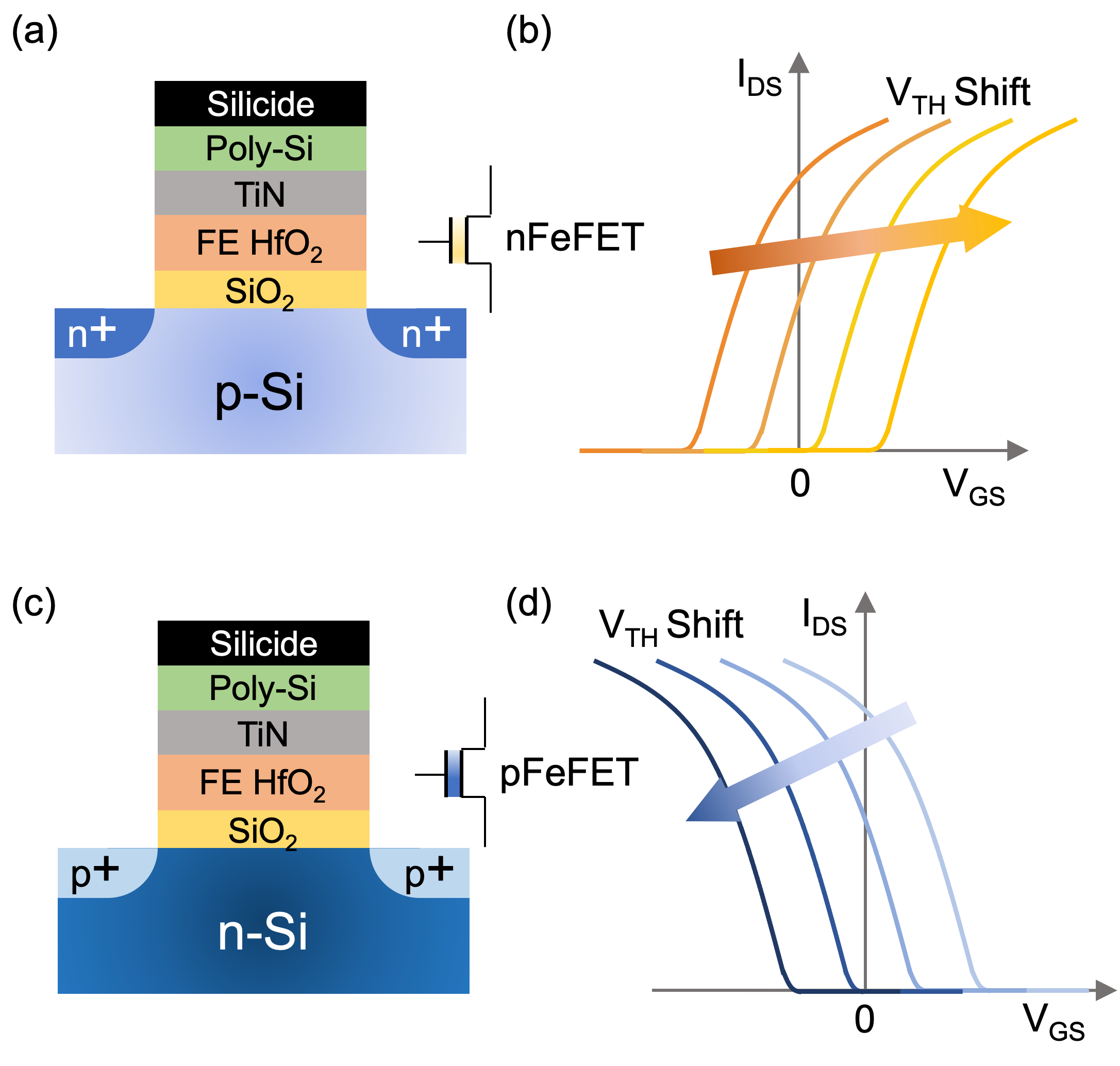
FeFETs are fabricated by integrating a ferroelectric layer at the gate stack of a MOSFET, as shown in Fig. 1(a)/(c). When a program voltage is applied to the gate, the degree and direction of polarization state of ferroelectric layer are set, making FeFETs non-volatile memory devices [21, 22, 23, 24]. The varying polarization states corresponding to different program voltage pulses applied at gate-source alter the threshold voltage () of the FeFETs per Fig.1(b),(d). It is through this characteristic that we achieve reconfigurable frequency multiplier designs. The characteristic curves of nFeFETs and pFeFETs resemble those of nMOS and pMOS transistors [25]. Note that nFeFETs and pFeFETs exhibit symmetrical characteristics, a crucial aspect in complementary FeFET frequency multipliers designs.
II-B Existing frequency multipliers
In [10], a planar Schottky diode based frequency doubler is proposed, offering an impressive maximum operating frequency of 220GHz. However, Schottky diode multipliers requires exceptionally high input signal power, i.e., 200mW, to achieve high multiplication efficiency due to the inherent passivity of diodes. Another type of conventional high-power frequency doubler based on MOSFET can achieve 26GHz output at the cost of a relatively large chip size (0.28) and power consumption (10mW) [17].
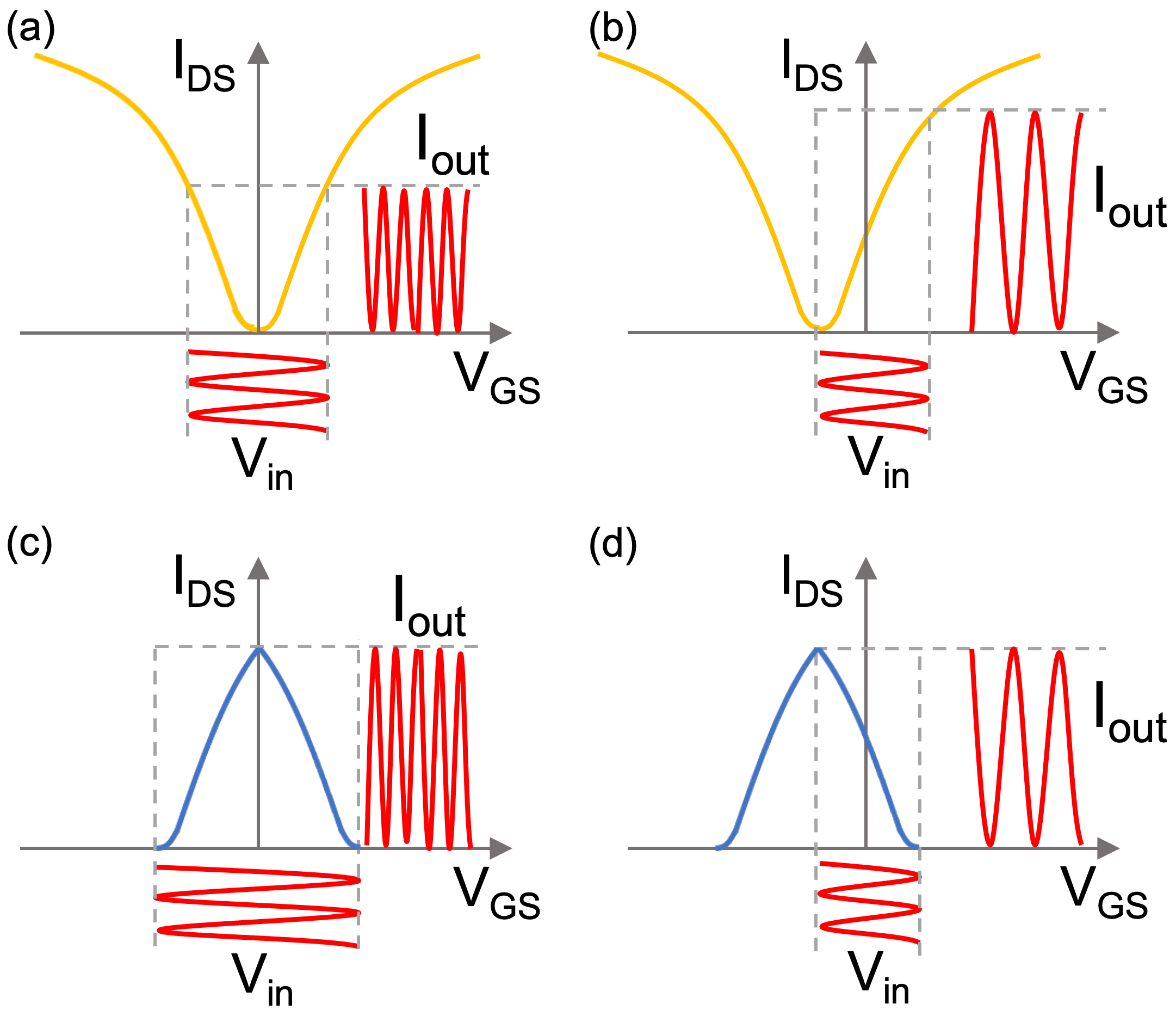
Emerging frequency multiplier designs harnessing the ambipolar parabolic characteristics of FeFET have been developed. In [18], modulation of a single FeFET’s ambipolar current was achieved by altering the drain () and/or gate voltage (), thereby approximating transfer characteristic of the FeFET to an ideal parabolic curve, thus enabling frequency doubling and signal transmission, respectively. The conceptual principles are illustrated in Fig. 2(a)/(b). However, in practice, the modulation of symmetrical ambipolar characteristic of the single FeFET requires costly tuning techniques, including accurately tuning the partial polarization switching and the band-to-band tunneling drain current, which are not easily realized. Consequently, asymmetric deviating from the ideal parabolic shape result in the generation of undesired harmonics. In [20], a vertical nanowire ferroelectric tunnel field-effect transistor (ferro-TFET) that exhibits a downward-opening parabolic transfer curve was employed as the multiplier device to accomplish frequency doubling and signal transmission, as depicted in Fig. 2(c)/(d). However, the fabrication of nanowire ferro-TFET devices is complex and costly, incompatible with traditional CMOS technology. The parabolic transfer characteristics of these devices are also facing the challenge of deviating from the symmetrical parabolic shape, leading to the generation of unwanted harmonics. In this paper, we propose to utilize the standard complementary FeFETs for efficient and economic designs with parabolic transfer characteristic, and further propose feasible and compact reconfigurable frequency multipliers with more multiplications.
III Proposed Reconfigurable frequency multipliers
In this section, we propose four 2FeFET structures implementing reconfigurable frequency multipliers. We further propose four reconfigurable multipliers realizing more harmonics.
III-A 2FeFET structures implementing multipliers
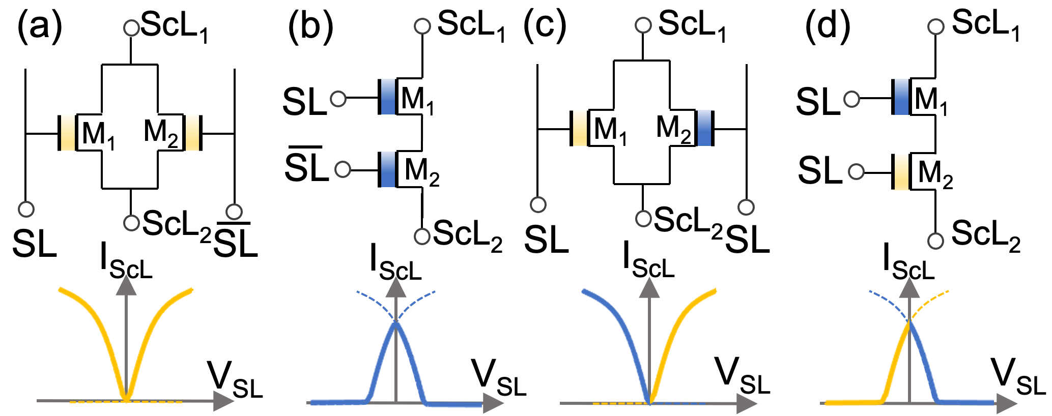
To address the asymmetrical parabolic characteristic or complex technology issues associated with prior ambipolar FeFET based designs, we propose to use two CMOS-compatible FeFETs based structures as below to capture single-parabola-shaped characteristics. As depicted in Fig.3(a), two nFeFETs are connected in parallel, with their gate voltages complementary to each other, i.e., . As a result, the - curves of the identical nFeFETs mirror to each other, and the combined transfer characteristic exhibits a symmetrical, upward-opening parabolic shape. On the contrary, two pFeFETs connected in series with complementary gate voltages as shown in Fig.3(b) yields a symmetrical, downward-opening parabolic transfer characteristic. Note that due to the serial connection, is first programmed to low as a transmission gate to allow programming . Then is programmed.
We also propose 2FeFET structures based on complementary FeFETs. As illustrated in Fig.3(c), nFeFET and pFeFET in parallel generates a relatively symmetrical, upward-opening parabolic characteristic. This structure eliminates complementary gate voltages, and can be easily tuned to maintain the parabolic symmetry. On the contrary, as demonstrated in Fig.3(d), nFeFET and pFeFET in series with the same gate voltage results in a relatively symmetrical, upward-opening parabolic characteristic. All four 2FeFET structures resemble symmetrical parabolic-shaped characteristic just like the ambipolar FeFET device discussed in [18, 20]. It can be readily seen that compared with ambipolar FeFETs, our proposed structures are built with CMOS-compatible FeFET devices without complex technology process, and the symmetrical parabolic characteristics can be simply obtained by identical nFeFETs, pFeFETs, or width ratio tuning between nFeFET and pFeFET. These structures represent a more general and economic way for the realizations of frequency multiplication.
The principles of our proposed 2FeFET structures for frequency multiplication are similar to that of ambipolar devices, as shown in Fig.2. When employing the 2nFeFETs or complementary FeFETs based structures that exhibit upward-opening parabolic curves as shown in Fig.3(a)/(c), we set the operating point at the minima of the parabola. When the input signal applied at transitions from the valley to the peak, the corresponding output current transitions from a peak to a valley, and back to a peak. Consequently, the output signal corresponds to a second harmonic (frequency doubling) of the input signal. Similarly, when employing the 2nFeFETs or complementary FeFETs based structures exhibiting a downward-opening parabola as shown in Fig.3(b)/(d), a second harmonic output signal can also be generated. As illustrated in Fig.2(b)/(d), tunable characteristics of FeFETs (see Fig.1) enable the shift of the parabolic curves. We then place the operating point of input signal at one branch of the curve. In this configuration, as the input signal transitions from a valley to a peak, the output signal also transitions from a valley to a peak, making the 2FeFET structures signal amplifiers.
Hereby, our proposed 2FeFET structures can achieve reconfigurable first and second harmonic generation. Yet, the potential of our proposal has not been fully exploited. To build general designs that perform scalable frequency multiplications, such as threefold or fourfold, relying solely on the 2FeFET structures with a single parabolic shapes is insufficient. Drawing inspiration from single parabolic curves, we naturally consider superimposing single-parabolic curves with an interval to create double-peak or double-valley shape curves, which can be easily implemented based on our proposed structures.
III-B Reconfigurable multipliers with more multiplications
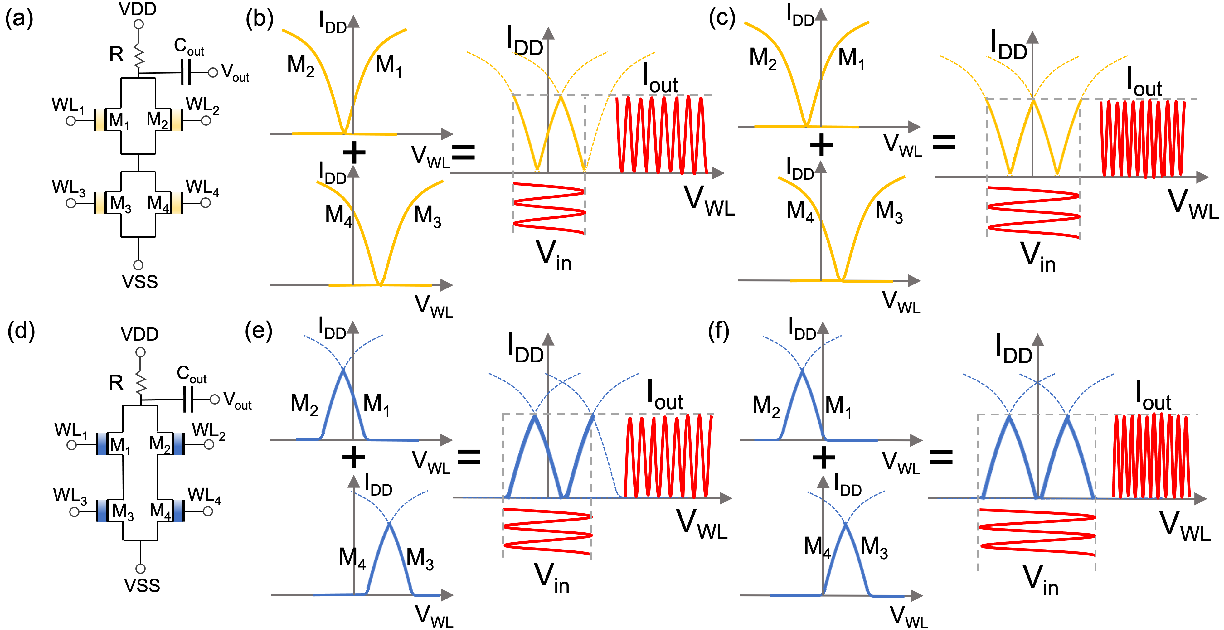
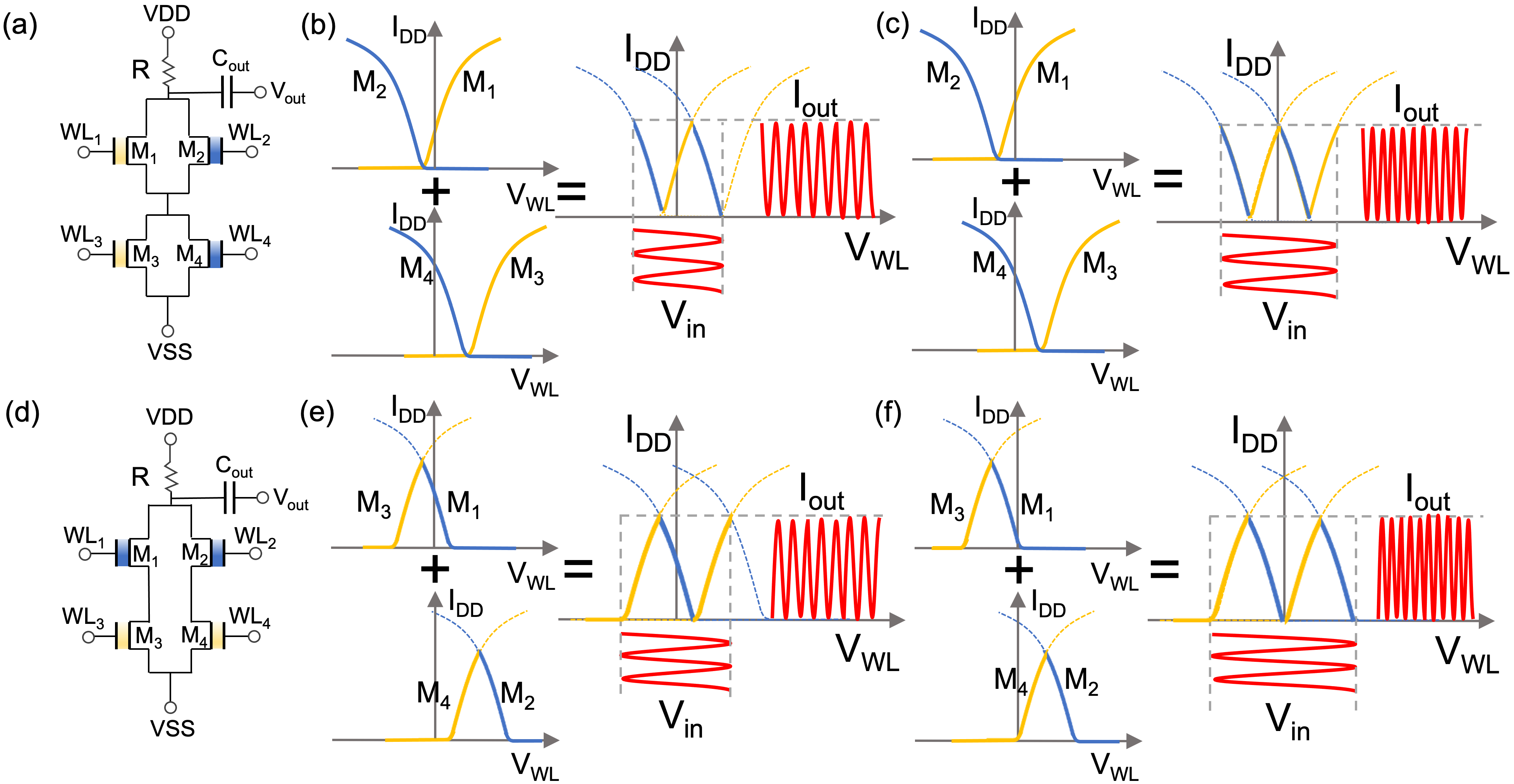
We further build four reconfigurable frequency multipliers that support multiple multiplication modes, i.e., first harmonic (First-H), second harmonic (Second-H), third harmonic (Third-H) and fourth harmonic (Fourth-H), based on previously discussed 2FeFET structures. As depicted in Fig.4(a), we place two parallel connected 2nFeFET structures (Fig.3(a)) in series. The gate voltages of and are complementary, i.e., . We refer to this structure as the 4n-serial design. As a result, two upward-opening parabolic curves are superimposed through the “AND” logic, forming a double-valley shape of transfer characteristic as shown in Fig.4(b)/(c). The slight interval between the superimposed upward-opening parabolic curves can be realized by programming the threshold voltages of 4 nFeFETs. During the write, and are first programmed to low state, passing high voltage to drains of and , respectively. The gates of and are then applied with program pulses, followed by programming and .
As illustrated in Fig.4(b), programming the 4nFeFETs can shift the superimposed double-valley shape curve, such that the amplitude of input signal covers a valley and a peak within the double valley, with the midpoint aligning with the operating point of input signal. As the input signal goes from the valley to the peak, the corresponding output signal transitions between the peak and the valley within the superimposed curve for three times, achieving a threefold frequency multiplication, i.e., Third-H. The principle for achieving fourfold frequency multiplication is similar, as illustrated in Fig.4(c). The superimposed double-valley curve is programmed such that the amplitude of input signal covers two valleys and one peak, with the midpoint aligning with the operating point of input. As the input signal transitions from the valley to the peak, the corresponding output transitions between the peak and the valley within the double-valley curve for four times, generating the fourth harmonic signal. The Third-H and Fourth-H generations are determined by the shape of superimposed curve, the operating point and the amplitude of input. Similar operations can be applied to other three multiplier designs, and more multiplication modes can be proposed following above principles.
As depicted in Fig.4(d), we build another multiplier by placing two serial connected 2pFeFET structures (Fig.3(b)) in parallel. The gate voltages of and are complementary, i.e., . We refer to this structure as the 4p-parallel design. Two downward-opening parabolic curves are superimposed through the “OR” logic, forming the double-peak shape transfer characteristic. The interval between downward-opening parabolic curves can be realized by programming the of pFeFETs. During the write, and are first programmed to low state, passing high voltage to drains of and , respectively. The gates of and are then applied with program pulses, followed by programming and . The operation principles for Third-H and Fourth-H generations are similar to that of 4n-serial design, and illustrated in Fig.4(e)/(f).
The 4n-serial and 4p-parallel designs consume extra circuitry for complementary voltages. We hereby propose two multiplier designs to eliminate complementary voltages. As depicted in Fig.5(a), we place two parallel connected nFeFET and pFeFET structures (Fig.3(c)) in series. We refer to this structure as the n/p-serial design. Similar to the 4n-serial design, this n/p-serial design achieves a double-valley shape curve, and realizes frequency multiplications, i.e., Third-H and Fourth-H generations as illustrated in 5(b)/(c). Alternatively, as depicted in Fig.5(d), we place two serial connected nFeFET and pFeFET structures (Fig.3(d)) in parallel to achieve the double-peak shape curve. We refer to this structure as the n/p-parallel design. Frequency multiplication principles are illustrated in Fig.5(e)/(f).
Overall, we propose above four designs supporting multiple frequency multiplications, i.e., First-H, Second-H, Third-H and Fourth-H generations, as representatives of scalable frequency multiplier design methodology. Based on the 2FeFET structures, we can construct multipliers with more harmonic modes.
| [17] | [18] | [20] | 4n-serial | 4p-parallel | n/p-serial⋆ | n/p-parallel⋆ | |
| Sturcture | 5R-11C-8L-3T | 1R-1C-1T | 1R-1T | 1R-1C-4T | 1R-1C-4T | 1R-1C-4T | 1R-1C-4T |
| Device | CMOS | ambipolar FeFET | ambipolar FeFET | FeFET | FeFET | FeFET | FeFET |
| Area() | 280000 | 0.21 | 0.01 | 0.0256 | 0.0448 | 0.182 | 0.190 |
| Max Frequency(MHz) | 20000 | 1 | 0.01 | 5000 | 10000 | 100 | 1000 |
| Power(W) | 20000 | 4.8 | 0.00151 | 3.35 | 3.12 | 8.05 | 9.34 |
| Supply Voltage(V) | 2.6 | 3.5 | 0.5 | 1 | 1 | 1 | 1 |
| Multiplication | x2 | x1,x2 | x1,x2 | x1,x2,x3,x4 | x1,x2,x3,x4 | x1,x2,x3,x4 | x1,x2,x3,x4 |
| Reconfigurablility | no | yes | yes | yes | yes | yes | yes |
: Eliminating the complementary voltage generator circuitry.
IV Validations and Evaluations
In this section, we validate the proposed frequency multipliers with various multiplication modes. We then evaluate and compare the designs with prior works. Finally, a case study of reconfigurable multiplier is demonstrated. 45nm Preisach FeFET model [26] is utilized in the Cadence simulations. The size of pFeFET is tuned to ensure that the conducting current is nearly the same as that of nFeFET.
IV-A Frequency multiplier validations and comparisons
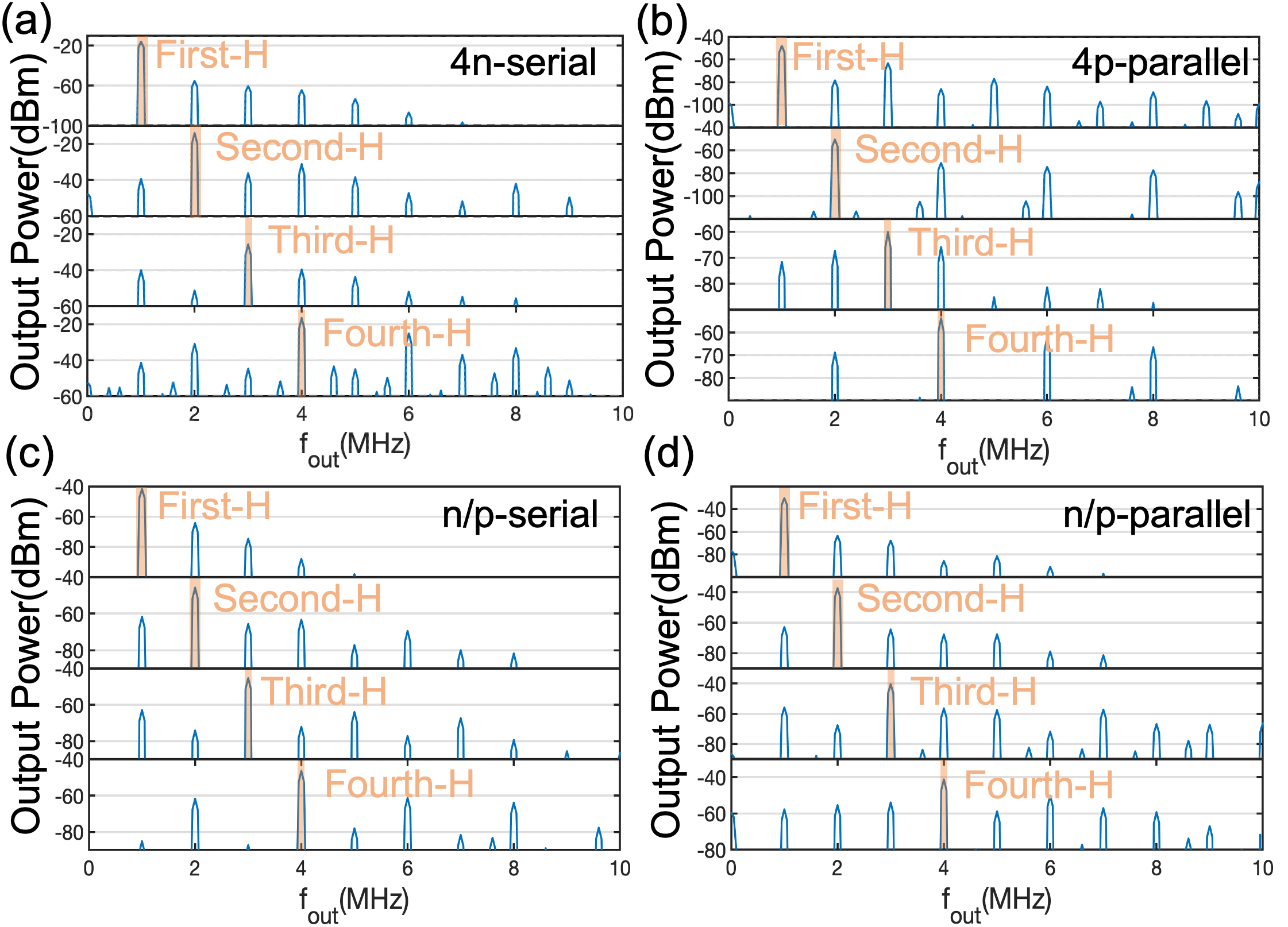
We validate the frequency multiplication functions of our proposed reconfigurable multipliers. Fig.6 presents the output power spectrum of the four proposed designs in different frequency multiplication modes. It can be observed that all four designs confirm their frequency multiplication functionality. Although non-ideal transfer characteristics inevitably lead to extra harmonics, the output power of target harmonic frequency is at least 10dBm higher compared to other harmonic components.
The maximum operating frequency represents the capability of multipliers. Taking frequency quadrupling as an example. As shown in Fig.7, for the 4n-serial design, when the input signal frequency exceeds 5GHz, the Fourth-H component starts to decline, and the First-H dominates by the time it reaches 10GHz. The 4p-parallel design functions well even at 10GHz of input signal, but when the input frequency reaches 100GHz, the Second-H starts to dominate. As for the n/p-serial design, its maximum operating frequency is 0.1GHz, while for the n/p-parallel structure, the maximum operating frequency is 1GHz.
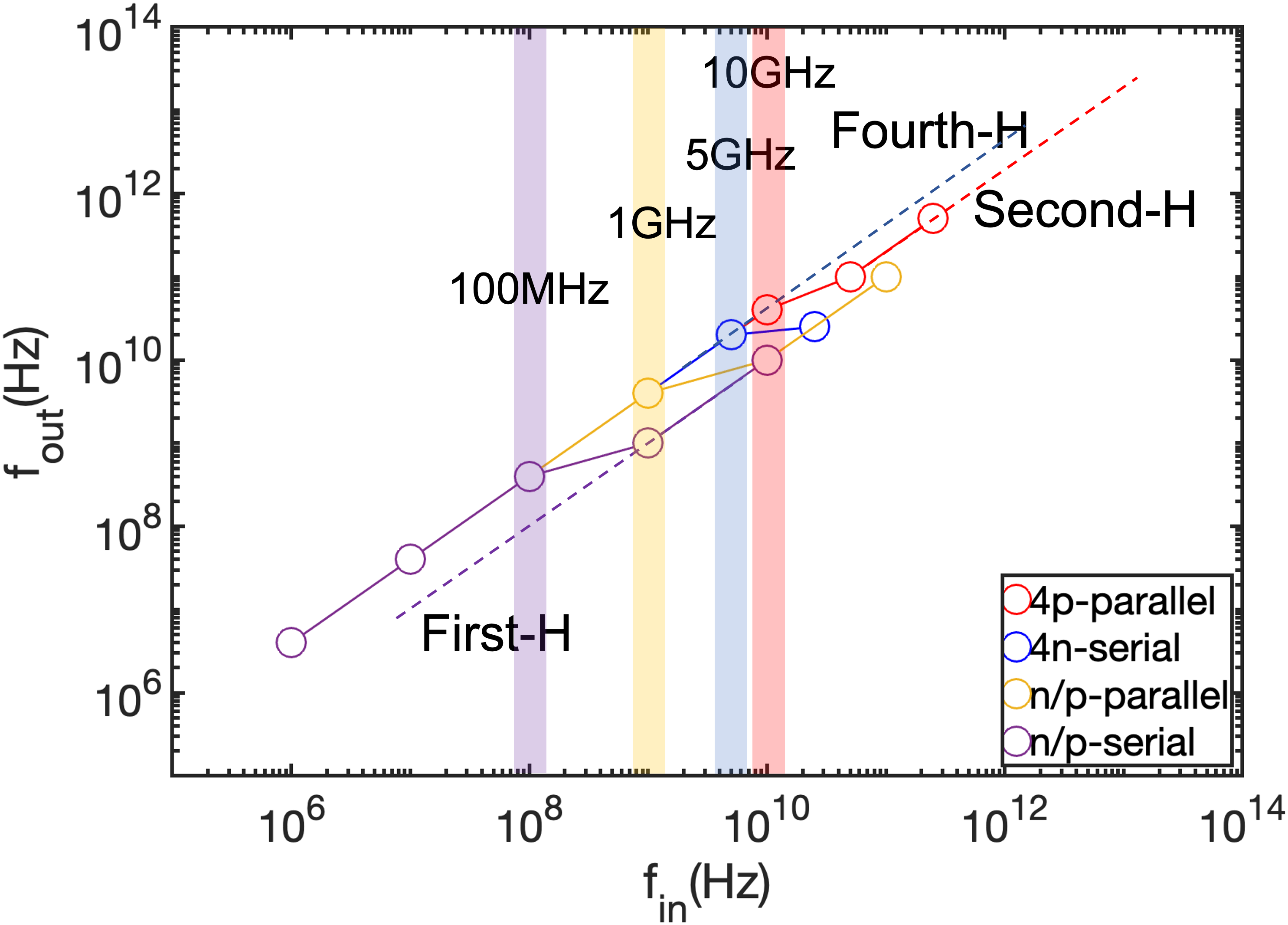
Table I summarizes the performance metrics of the proposed and existing frequency multipliers. It is evident that, compared to traditional CMOS multipliers[17], the reconfigurable multipliers based on FeFETs offer the advantages of smaller area and extremely low power consumption. However, the maximum operating frequencies of the reconfigurable multipliers in [18, 20] are much lower than those of traditional multipliers. Our proposed four reconfigurable multipliers have much higher maximum operating frequencies than those in [18, 20]. Furthermore, the maximum operating frequency of the 4p-parallel design approaches that of traditional CMOS multipliers. All four proposed reconfigurable multipliers offer four different frequency multiplication modes (and potentially more modes given the scalability), surpassing traditional multipliers with fixed multiplication mode [17] and the two modes in [18, 20].
IV-B Case study: Frequency Shift Keying
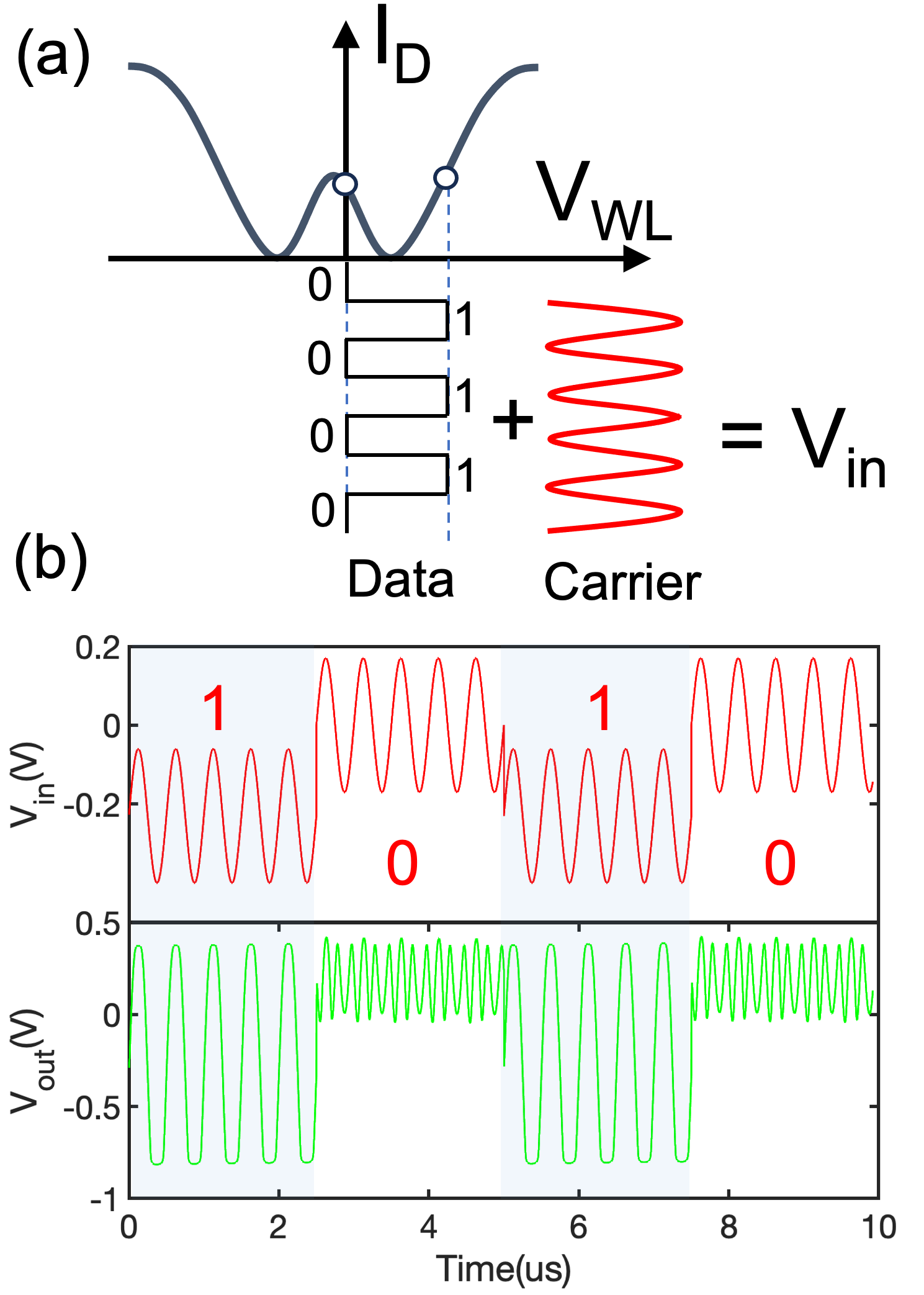
We showcase that our proposed frequency multiplier designs can achieve frequency shift keying (FSK) functionality, which is widely used in communication systems [27]. The FSK can be implemented by applying the data pulses and carrier signals at the input of our multipliers, i.e., . The valley and the peak of data pulses are aligned with the operating points of the multipliers as depicted in Fig.8(a), respectively. When the data signal is at ’1’ level, the input signal oscillates at the operating point that achieves First-H, i.e., signal transmission. When the data signal is at ’0’ level, aligning with the operating point that achieves Third-H, the output frequency is triple of input. In this way, the output frequency periodically shifts between single frequency and triple frequency, as shown in Fig.8(b). As can be seen, the alignment of data pulses with the operating points within the transfer curve of multipliers is the key enabler of FSK. This alignment can be realized by adjusting the peak/valley amplitude of data pulses and carrier signal, while maintaining the FeFET programming configurations. However, this method can only achieve the frequency shifts between single and double/triple/quadruple frequencies, as well as the shift between double and quadruple frequencies111Aligning the valley/peak of data pulses with the operating points corresponding to Second-H (Fig.2(a)/(c))/Fourth-H (Fig.4(c)/(f)) and (Fig.5(c)/(f)).. Altering the FeFET programming configuration of multipliers, on the contrary, can generally achieve the shifts between any frequency modes, while consuming extra programming time.
V Conclusion
We exploit the programmable characteristics of complementary FeFETs to build four 2FeFET structures for reconfigurable frequency doubling and signal transmission functions. These 2FeFET structures resemble similar parabolic-shape curves to prior ambipolar FeFETs, while requiring much simpler technology and characteristic tuning. Based on 2FeFET structures, four novel reconfigurable frequency multipliers allowing for seamless switching between frequency multiplication modes are proposed. The performance of the propsoed multipliers are evaluated, and an example case of FSK is demonstrated. As emerging FeFETs continue to evolve, this work will provide insights to more compact, efficient and flexible frequency multiplier designs with enhanced multiplication modes compared to traditional counterparts and existing designs.
Acknowledgements
This work was supported in part by NSFC (92164203, 62104213), Zhejiang Provincial Natural Science Foundation (LD21F040003, LQ21F040006), National Key R&D Program of China (2022YFB4400300).
References
- [1] M. Lanza et al., “Memristive technologies for data storage, computation, encryption, and radio-frequency communication,” Science, vol. 376, no. 6597, p. eabj9979, 2022.
- [2] U. J. Lewark et al., “Mmic-based module-level frequency generation for e-band communication systems,” pp. 85–87, 2014.
- [3] H. Zheng et al., “Coarray tensor direction-of-arrival estimation,” IEEE Transactions on Signal Processing, vol. 71, pp. 1128–1142, 2023.
- [4] S. Abdulazhanov et al., “Reconfigurable ferroelectric hafnium oxide fefet fabricated in 28 nm cmos technology for mmwave applications,” in ESSDERC, pp. 113–116, IEEE, 2023.
- [5] A. Maestrini, J. Ward, G. Chattopadhyay, E. Schlecht, and I. Mehdi, “Terahertz sources based on frequency multiplication and their applications,” Frequenz, vol. 62, no. 5-6, pp. 118–122, 2008.
- [6] G. Chien and P. Gray, “A 900-mhz local oscillator using a dll-based frequency multiplier technique for pcs applications,” IEEE JSSC, vol. 35, no. 12, pp. 1996–1999, 2000.
- [7] D. Thomas and G. Branner, “Optimization of active microwave frequency multiplier performance utilizing harmonic terminating impedances,” IEEE TMTT, vol. 44, no. 12, pp. 2617–2624, 1996.
- [8] U. R. Pfeiffer et al., “Schottky barrier diode circuits in silicon for future millimeter-wave and terahertz applications,” IEEE TMTT, vol. 56, no. 2, pp. 364–371, 2008.
- [9] C. Mishra et al., “Silicon schottky diode power converters beyond 100 ghz,” in 2007 IEEE RFIC Symposium, pp. 547–550, 2007.
- [10] P. Chen et al., “A 220ghz frequency doubler based on plannar schottky diodes,” pp. 1–2, 2013.
- [11] M. Abbasi et al., “Single-chip frequency multiplier chains for millimeter-wave signal generation,” IEEE TMTT, vol. 57(12), pp. 3134–3142, 2009.
- [12] E. Monaco et al., “Injection-locked cmos frequency doublers for -wave and mm-wave applications,” IEEE JSSC, vol. 45(8), pp. 1565–1574, 2010.
- [13] C. Mao et al., “125-ghz diode frequency doubler in 0.13- cmos,” IEEE JSSC, vol. 44, no. 5, pp. 1531–1538, 2009.
- [14] U. R. Pfeiffer et al., “Schottky barrier diode circuits in silicon for future millimeter-wave and terahertz applications,” IEEE TMTT, vol. 56, no. 2, pp. 364–371, 2008.
- [15] C. Mao et al., “Millimeter wave varistor mode schottky diode frequency doubler in cmos,” IEEE MWCL, vol. 19, no. 3, pp. 173–175, 2009.
- [16] D. Shim et al., “150 ghz complementary anti-parallel diode frequency tripler in 130 nm cmos,” IEEE MWCL, vol. 21, no. 1, pp. 43–45, 2011.
- [17] J.-H. Chen et al., “A high gain, high power k-band frequency doubler in 0.18 cmos process,” IEEE MWCL, vol. 20(9), pp. 522–524, 2010.
- [18] H. Mulaosmanovic et al., “Reconfigurable frequency multiplication with a ferroelectric transistor,” Nature Electronics, vol. 3(7), pp. 391–397, 2020.
- [19] H. Xu et al., “On the challenges and design mitigations of single transistor ferroelectric content addressable memory,” IEEE EDL, 2023.
- [20] Z. Zhu et al., “Reconfigurable signal modulation in a ferroelectric tunnel field-effect transistor,” Nature Communications, vol. 14(1), p. 2530, 2023.
- [21] X. S. Hu et al., “In-memory computing with associative memories: A cross-layer perspective,” in IEDM, pp. 25–2, IEEE, 2021.
- [22] T. Soliman et al., “Ultra-low power flexible precision fefet based analog in-memory computing,” in 2020 IEEE IEDM, pp. 29.2.1–29.2.4, 2020.
- [23] X. Yin et al., “An ultracompact single-ferroelectric field-effect transistor binary and multibit associative search engine,” Adv. Intelli. Syst., p. 2200428, 2023.
- [24] Q. Huang et al., “Fefet based in-memory hyperdimensional encoding design,” IEEE TCAD, 2023.
- [25] S. Deng et al., “Unraveling the dynamics of charge trapping and de-trapping in ferroelectric fets,” IEEE TED, vol. 69(3), pp. 1503–1511, 2022.
- [26] K. Ni et al., “A circuit compatible accurate compact model for ferroelectric-fets,” in IEEE symp. on VLSI, pp. 131–132, IEEE, 2018.
- [27] B. Watson, “Fsk: signals and demodulation,” Watkins–Johnson Company Tech–notes, vol. 7, no. 5, 1980.