Photonic crystal cavity IQ modulators in thin-film lithium niobate for coherent communications
Abstract
Thin-Film Lithium Niobate (TFLN) is an emerging integrated photonic platform showing great promise due to its large second-order nonlinearity at microwave and optical frequencies Boyd (2008), cryogenic compatibility Lomonte et al. (2021), large piezoelectric response Maleki and Matsko (2009), and low optical loss at visible Desiatov et al. (2019) and near-infrared Zhang et al. (2017) wavelengths. These properties enabled Mach-Zehnder interferometer-based devices to demonstrate amplitude- Wang et al. (2018a) and in-phase/quadrature (IQ) Xu et al. (2022) modulation at voltage levels compatible with complementary metal-oxide-semiconductor (CMOS) electronics. Maintaining low-voltage operation requires centimeter-scale device lengths, making it challenging to realize the large-scale circuits required by ever-increasing bandwidth demands in data communications Cheng et al. (2018). Reduced device sizes reaching the 10 m scale are possible with photonic crystal (PhC) cavities. So far, their operation has been limited to modulation of amplitudes and required circulators Li et al. (2020a) or lacked cascadability Prencipe et al. (2021). Here, we demonstrate a compact IQ modulator using two PhC cavities operating as phase shifters in a Fabry-Perot-enhanced Michelson interferometer configuration Shoemaker et al. (1991). It supports cascadable Xu et al. (2006) amplitude and phase modulation at GHz bandwidths with CMOS-compatible voltages. While the bandwidth limitation of resonant devices is often considered detrimental, their compactness enables dense co-integration with CMOS electronics where clock-rate-level operation (few GHz) removes power-hungry electrical time-multiplexing Miller (2017); Lee et al. (2023). Recent demonstrations of chip-scale transceivers with dense-wavelength division multiplied transceivers Rizzo et al. (2023) could be monolithically implemented and driven toward ultimate information densities using TFLN electro-optic frequency combs Hu et al. (2022) and our PhC IQ modulators.
I Introduction
Modern telecommunications rely on electro-optic (EO) modulators to convert information between electrical and optical signals Sinatkas et al. (2021); Liu et al. (2004); Xu et al. (2005); Reed et al. (2010); Timurdogan et al. (2014); Han et al. (2017); Hiraki et al. (2017); Pintus et al. (2022); Xiong et al. (2012); Wang et al. (2018a); Abel et al. (2019). The exponentially increasing demand for information capacity Winzer and Neilson (2017) and growing interest in networking superconducting quantum circuits Xiang et al. (2013) motivates the development of small-footprint EO modulators with low power consumption that can be densely integrated with electronic processors Miller (2017) while operating near the fundamental limits given by the interaction between microwave and optical photons Han et al. (2021). Coherent communications have proven instrumental in leveraging existing technology for high bandwidth internet protocol optical routing Rohde et al. (2014); Agrell et al. (2016) and enhancing throughput in long-haul fiber networks Schmogrow et al. (2012); Pfeifle et al. (2014); Kikuchi (2016); Wang et al. (2018b), while promising similar features for data center interconnects and edge computing Cheng et al. (2018); Sludds et al. (2022).
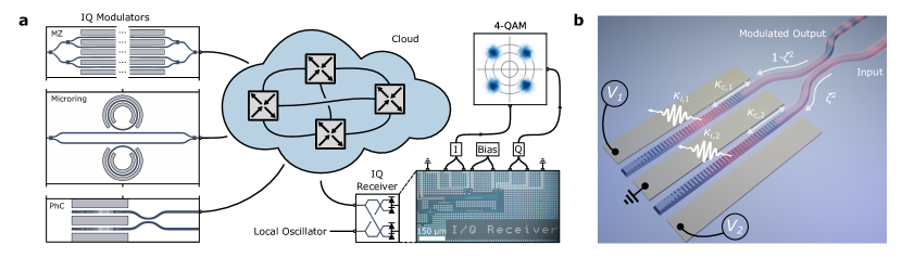
As illustrated in Fig. 1a, these advances in coherent communications hinge on in-phase/quadrature (IQ) modulators, which are able to control both the amplitude and phase of optical fields and are currently sustained by commercially available InP-based devices Rouvalis (2015); Ozaki et al. (2018).
Further technological requirements have driven rapid advances in photonic integrated circuits (PICs) with EO modulators Sinatkas et al. (2021) based on interactions including free-carrier dispersion Liu et al. (2004); Xu et al. (2005); Reed et al. (2010); Timurdogan et al. (2014), the quantum confined Stark effect Han et al. (2017); Hiraki et al. (2017); Pintus et al. (2022), and the Pockels effect Xiong et al. (2012); Wang et al. (2018a); Abel et al. (2019). Advances in silicon photonics have notably enabled a new generation of coherent optical engines Novack et al. (2018); Nokia (2023) along with more compact implementations relying on microring phase shifters Dong et al. (2012). Such free carrier-based devices face fundamental trade-offs between insertion loss and modulation efficiency that ultimately cap their performance. The pure phase response of Pockels materials can overcome these challenges. For example, thin-film lithium niobate (TFLN) is a promising PIC platform due to its wide transparency window, large Pockels coefficients , and low waveguide loss Wang et al. (2018a). When arranged in a traveling-wave Mach-Zehnder configuration, TFLN modulators achieve modulation rates exceeding 100 GHz Wang et al. (2018a); Xu et al. (2020, 2022); Kharel et al. (2021) and can naturally integrate into IQ modulator architectures Xu et al. (2020, 2022). However, as emphasized in Fig. 1a, their length needs to extend over several millimeters to reach sufficient microwave-to-optical interaction strengths, which could prevent their use in applications requiring high co-integration densities. The modulator size has been reduced using structures such as folded Michelson interferometers Xu et al. (2019) and microring-assisted Mach-Zehnder interferometers Feng et al. (2022); Menssen et al. (2023). Dielectric photonic crystal (PhC) cavities provide wavelength-scale confinement without compromising insertion loss. As shown in a recent demonstration of off-keying in TFLN PhC cavities Li et al. (2020a), this resonant modulation scheme preserves the alignment between LN’s Pockels tensor and the modulating electric field over a device with an ultra-small capacitance and an optical mode volume as low as 0.58 µm3. However, it has remained an open challenge to develop devices with 2 degrees of freedom – the minimum needed for arbitrary modulation of the two field quadratures.
Here, we solve this challenge by introducing an ultrasmall TFLN PhC IQ modulator, taking advantage of wavelength-scale confinement through PhC cavities in an interferometric configuration. We demonstrate four symbol quadrature- and amplitude modulation (4-QAM) with a complementary-metal-oxide-semiconductor (CMOS) compatible peak-to-peak driving voltage of 2 V. The modulation rate of GHz is limited by the cavity quality factor () of , and our electrode configuration results in a tuning efficiency of GHz/V. Through iterative co-design and testing of cavity Bragg mirrors and stable fabrication process control in wafer-scale TFLN manufacturing, we achieve a fabrication yield exceeding 64% for PhCs with values above across devices with design parameters specified in the Supplementary.
II Results
The conventional ring-resonator-enhanced Mach-Zehnder architecture Dong et al. (2012); Feng et al. (2022); Menssen et al. (2023) does not carry over to PhC cavities, as they couple the incident field to forward- and backward-propagating waves. We therefore developed a different design: a cavity-assisted on-chip Michelson interferometer, inspired by laser interferometric gravitational wave detectors Shoemaker et al. (1991) that use two arms of one-sided Fabry Perot cavities. In our design, a directional coupler with a : splitting ratio distributes an input optical signal to two one-sided Fabry-Perot PhC cavities where light couples to the waveguides at rates and , see Fig. 1b.
Pairs of electrodes apply electric fields across the TFLN cavities by means of the voltages and . To first order in , the cavity resonance frequencies shift by (see Supplementary Section II)
| (1) |
where is the resonance at zero voltage, and is the tuning efficiency. Cavity loss is described by the intrinsic decay rates and . After reflection from the cavities, the modulated signals travel back across the directional coupler and interfere. The input-output transmission is (see Supplementary Section III)
| (2a) | ||||
| (2b) | ||||
where is the cavity reflection coefficient, is the detuning from the input carrier frequency, is the total linewidth, and describes the relative phase between the interferometer arms. The transmission attains any complex value within the unit circle in the limit of highly over-coupled cavities () with a 50:50 directional coupler. The condition for complete extinction () is independent of the splitting ratio , which is not the case for Mach-Zehnder implementations containing two distinct couplers.
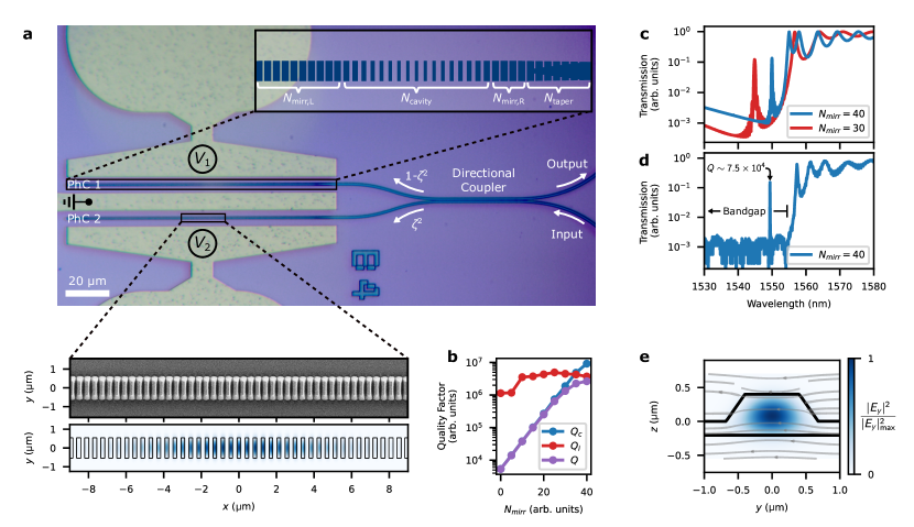
Figure 2a shows a micrograph of our fabricated TFLN IQ modulator. The top-right inset sketches the PhC cavity to illustrate its formation by modulating the width of a waveguide. As detailed in Supplementary Section IV, we vary the duty cycle parabolically over periods to produce a high resonance Quan et al. (2010). Placing fewer mirror periods on the side facing the waveguide () achieves a one-sided configuration. A smooth transition to the propagating waveguide mode minimizes out-of-plane scattering by linearly reducing the width modulation to zero over periods. Figure 2b plots the total- (purple), coupling- (blue), and intrinsic (red) quality factors, calculated using finite-difference-time-domain (FDTD) simulations, as a function of the number of mirror periods for a two-sided cavity (). It highlights how is easily adjusted to match a targeted modulation speed without sacrificing the intrinsic quality factor . The corresponding simulated transmission spectra are shown in Fig. 2c, and the measured spectrum from a two-sided reference cavity is plotted in Fig. 2d. The good agreement between measurement and simulation (blue curves in Figs. 2c,d) results from extracting geometrical information via scanning-electron-microscope images and additional reference structures (see Supplemental Section V for details).
We calculate a tuning efficiency of GHz/V via first-order perturbation theory based on the overlap between the optical cavity mode and the field from the electrodes (see Supplementary Section VI). Figure 2e shows how the electrode field (streamlines) and the optical field (blue contour) are parallel to maximize their overlap.
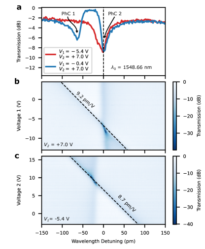
Experimentally, we determine the tuning efficiency by measuring the transmission at different voltage settings. Figure 3a plots two spectra with the resonances aligned (red) or separated (blue). Maps of transmission versus frequency and voltage across one of the cavities are shown in Figs. 3b,c. The transmission dips caused by cavity resonances are observed to shift linearly in response to the applied voltage. As described in Supplementary Section VII, we fit the data from Figs. 3b,c to Eq. (2), thereby obtaining the model parameters listed in Table 1.
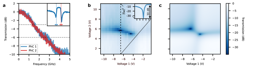
Figure 4a plots the small-signal modulator response when each PhC cavity is driven by a sinusoidal voltage signal. We choose the DC voltage offsets and laser wavelength to maximize the signal-to-noise of the transmitted light (see inset). Each cavity has a 3 dB cutoff around 1.5 GHz, which matches well with the fitted decay rates listed in Table 1.
| Cavity 1 | Cavity 2 | ||
| 1548.60 nm | 1548.71 nm | ||
| GHz | GHz | ||
| 0.46 | 1.42 | ||
| GHz/V | GHz/V | ||
| Michelson Interferometer | |||
To better understand how to set DC bias voltages for QAM modulation, we measure the transmission as a function of both voltages at a fixed laser wavelength. The result is shown in Fig. 4b, and Fig. 4c plots the simulated transmission map from Eq. (2a) using the parameters in Table 1. Destructive interference between the signals reflected from the two PhC cavities gives rise to the local minima exhibiting more than 30 dB extinction.
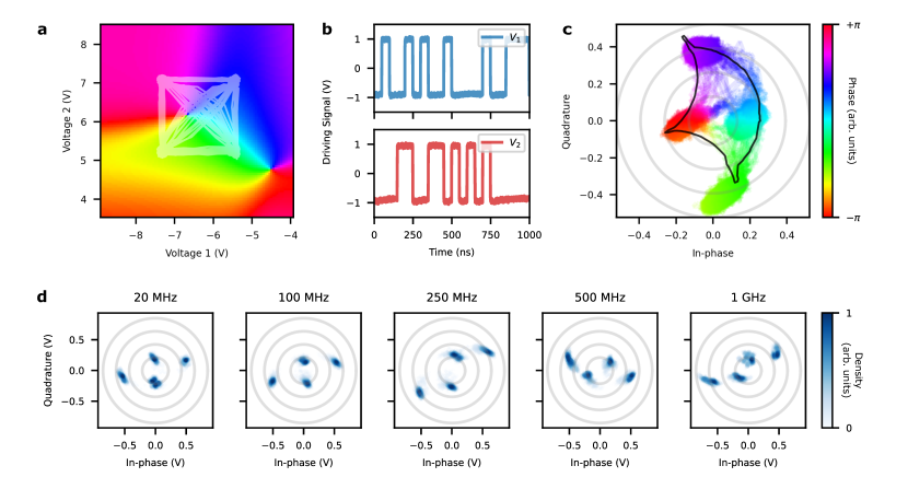
The good agreement between measurement and modeling allows us to use the transmission phase calculated from Eq. (2a) to set the DC-bias point at VV) while applying a radio-frequency (RF) modulation of 1 V to each cavity. Figure 5a plots this phase map, and the RF voltages of a pseudo-random bit sequence with symbols are plotted with semi-transparent white lines. Notice the large phase variations in the region between the two singularity points corresponding to the transmission minima in Fig. 4c. Separated minima are only possible when the cavities are sufficiently close to being over-coupled. Figure 5b plots the voltages of a subset of the applied bit sequence for an example with a 20 MHz repetition rate. We collect the IQ-modulated signal by a lensed fiber and detect it using a silicon-photonics integrated IQ receiver (see Supplementary Section VIII). In Fig. 5c, we plot the measured raw coherent transmission trace of a continuous wave (CW) input field modulated over a time span of 6.5 µs. Sampling the clustered points in Fig. 5c allows the reconstruction of the modulated field’s constellation diagram. We opt for a 1 GHz sampling frequency instead of the repetition rate of the driving pulses to consider a consistent amount of samples across the full set of modulation frequencies. Figure 5d provides such diagrams for modulation frequencies of 20 MHz, 100 MHz, 250 MHz, 500 MHz, and 1 GHz. Our results feature good data clustering at four distinct symbols exhibiting error vector magnitudes below 0.27 (see Methods) up to driving frequencies approaching the 3 dB cutoff of our IQ modulator. As discussed in Supplementary Section IX, optimized symbol separation is possible with more advanced encoding to account for the nontrivial dependence of on and . Such optimization procedures can also determine minimum device metrics for running coherent modulation processes. For example, given the insertion loss of our device, we require PhC cavity quality factors of at least to run the 4-QAM experiments shown in this work. This condition determined our reported cavity fabrication yield of 64%.
III Discussion
The compact size of our IQ modulator allows its energy consumption to be limited by its capacitance. This is a key requirement for low energy information processing Miller (2017) based on attojoule optoelectronics that could benefit emerging applications in photonics-based edge computing and inference Sludds et al. (2022). As discussed in Supplementary Section IV, we estimate an average value of 25.8 fJ per bit, though it could be reduced below 1 fJ/bit by appropriate design modifications Li et al. (2020a). Compact and energy-efficient modulators reopens the trade space comprised by multiplexing in the temporal, spatial, and spectral domains Lee et al. (2023). The moderate bandwidth of energy-efficient high- resonant modulators need not be a drawback since operating at a few GHz avoids power-hungry tasks such as electronic serialization Miller (2017) as well as clock and data recovery. For instance, a recent demonstration used silicon microring resonators for amplitude-modulation of 32 wavelength channels generated from a single laser using a silicon-nitride Kerr comb Rizzo et al. (2023). Similar TFLN implementations could monolithically integrate electro-optic combs Hu et al. (2022) and our PhC IQ modulators to reduce footprint further and eliminate chip-to-chip coupling loss. Importantly, our PhC IQ modulators are cascadable like rings Rizzo et al. (2023) since the transmission approaches 1 away from the resonances when and . The TFLN platform also benefits from recently introduced components, such as on-chip lasers Shams-Ansari et al. (2022); Guo et al. (2023); Snigirev et al. (2023), amplifiers Chen et al. (2021), and isolators Yu et al. (2023). Compact multiport switches were also proposed based on one-sided PhC cavity phase modulators Heuck (2023).
Reducing the interaction volume of electro-optic coupling between optical and RF fields and TFLN’s cryogenic compatibility Lomonte et al. (2021) introduces new prospects for quantum computing and networking, especially between microwave and optical single photons. Current implementations rely on coupled racetrack cavities McKenna et al. (2020); Holzgrafe et al. (2020) with footprints that could be reduced by several orders of magnitude by switching to PhC cavities. Electro-optic control over tightly confined optical cavity modes was proposed for nonlinear quantum information processing Heuck et al. (2020); Li et al. (2020b); Krastanov et al. (2021) and would similarly benefit systems with integrated quantum emitters Yang et al. (2023).
Future work should focus on stabilizing the optical response of our devices. Such considerations include minimizing transmission drifts due to photorefractive effects, which are known to be significant in TFLN cavities Zhu et al. (2021). Mitigation strategies include cladding removal Xu et al. (2021), elevated operating temperature Yariv et al. (1996); Rams et al. (2000), and doping Wang et al. (2018c); Jankowski et al. (2020); Kong et al. (2020). For classical interconnect applications with significant variations in operating temperature, feedback control loops will be necessary Christen et al. ; Lee et al. (2023); Rizzo et al. (2023). Machine learning-assisted state-estimation Lohani et al. (2020); Danaci et al. (2021); Lohani et al. (2022, 2023) could play a crucial role in stabilizing the modulator’s transmission and replacing conventional discrete signal processing methods to address channel mixing in coherent communications. Future investigations should additionally include energy reductions by replacing ohmic heaters Lee et al. (2023); Rizzo et al. (2023) with non-volatile tuning mechanisms, such as phase-change materials Bente et al. (2023), electro-mechanical effects Jiang et al. (2020), or laser annealing of oxides Lee et al. (2009); Chen et al. (2011); Panuski et al. (2022).
In summary, we introduced an ultra-compact PIC-based electro-optic IQ modulator. By incorporating a pair of tunable PhC cavities in TFLN integrated photonics, we demonstrated GHz-rate coherent modulation of an optical field using CMOS-compatible driving voltages and a footprint of 40-by-200 µm2. Further size reduction is straightforward Li et al. (2020a), which will pave the way towards dense co-integrated CMOS electronics and optical IQ modulators for large-scale EO modulation.
IV Methods
Device Fabrication We fabricated our chip in one of CSEM’s TFLN multi-project fabrication runs based on a 600 nm thick -cut TFLN on insulator wafer from NanoLN. We etch the LN waveguides and PhCs using an HSQ mask patterned with electron-beam lithography. The etch is configured to remove 400 nm of LN and result in waveguides with a sidewall angle with respect to the normal of the chip. Within the gaps of the PhC’s Bragg mirrors, SEM imaging and modeling of measured transmission data reveal that the sidewall angle is closer to (see Supplemental Section V). We pattern 500 nm thick gold electrodes with a liftoff process. Waveguides are designed to have a width of 800 nm that tapers out to 900 nm once they reach the PhC region of the device. We use a 660 nm gap in our modulator’s directional coupler.
PhC Design Parameters We set the Bragg period in our IQ modulator’s PhC cavities to 426 nm and the number of Bragg periods in the input mirror to . The duty cycle of the Bragg mirrors is 68% and tapers up to 83% at the cavity center. We provide further details related to this tapering in Supplementary Section IV. For the experimental transmission measurements of the two-sided cavity shown in Fig. 2f, we show the results of the fabricated cavity with parameters most similar to our IQ modulator device. Here, the number of mirror periods is and the duty cycle of the cavity region is 80%, while the Bragg period and the duty cycle of the mirrors are the same.
Simulation parameters As specified by the fabrication process, our simulations assume a 600 nm thick TFLN membrane with a 400 nm ridge and a sidewall angle of attributed to the sides of the waveguide. We set the sidewall angles in the gaps formed by the Bragg structure to as approximated from SEM imaging and modeling. We provide further details on how these geometric parameters affect the transmission of the cavities in the Supplementary. We performed all finite-difference-time-domain (FDTD) simulations provided in this work with Ansys’s Lumerical tools. Bandgap wavelengths of infinite Bragg mirrors were simulated using MIT Photonic Bands (MPB). We performed all finite element method (FEM) simulations with COMSOL Multiphysics.
Error Vector Magnitude Calculation We rely on the following definition of the error vector magnitude (EVM) for each symbol of a constellation diagram:
where is the number of acquired samples attributed to a symbol, corresponds to the measured quadratures of the samples, and are the expected quadrature values of the symbol. The reported values attributed to a single constellation diagram correspond to the average EVMs across all of the diagram’s symbols.
References
- Boyd (2008) R. W. Boyd, Nonlinear Optics, 3rd ed. (Academic Press, Inc., USA, 2008).
- Lomonte et al. (2021) E. Lomonte, M. A. Wolff, F. Beutel, S. Ferrari, C. Schuck, W. H. P. Pernice, and F. Lenzini, Nature Communications 12, 6847 (2021).
- Maleki and Matsko (2009) L. Maleki and A. Matsko, Ferroelectric Crystals for Photonic Applications, 2nd ed. (Springer, Germany, 2009).
- Desiatov et al. (2019) B. Desiatov, A. Shams-Ansari, M. Zhang, C. Wang, and M. Lončar, Optica 6, 380 (2019).
- Zhang et al. (2017) M. Zhang, C. Wang, R. Cheng, A. Shams-Ansari, and M. Lončar, Optica 4, 1536 (2017).
- Wang et al. (2018a) C. Wang, M. Zhang, X. Chen, M. Bertrand, A. Shams-Ansari, S. Chandrasekhar, P. Winzer, and M. Lončar, Nature 562, 101 (2018a).
- Xu et al. (2022) M. Xu, Y. Zhu, F. Pittalà, J. Tang, M. He, W. C. Ng, J. Wang, Z. Ruan, X. Tang, M. Kuschnerov, L. Liu, S. Yu, B. Zheng, and X. Cai, Optica 9, 61 (2022).
- Cheng et al. (2018) Q. Cheng, M. Bahadori, M. Glick, S. Rumley, and K. Bergman, Optica 5, 1354 (2018).
- Li et al. (2020a) M. Li, J. Ling, Y. He, U. A. Javid, S. Xue, and Q. Lin, Nat. Commun. 11, 4123 (2020a).
- Prencipe et al. (2021) A. Prencipe, M. A. Baghban, and K. Gallo, ACS Photonics 8, 2923 (2021).
- Shoemaker et al. (1991) D. Shoemaker, P. Fritschel, J. Giaime, N. Christensen, and R. Weiss, Appl. Opt. 30, 3133 (1991).
- Xu et al. (2006) Q. Xu, B. Schmidt, J. Shakya, and M. Lipson, Opt. Express 14, 9431 (2006).
- Miller (2017) D. A. B. Miller, J. Lightwave Technol. 35, 346 (2017).
- Lee et al. (2023) B. G. Lee, N. Nedovic, T. H. Greer, and C. T. Gray, Journal of Lightwave Technology 41, 1152 (2023).
- Rizzo et al. (2023) A. Rizzo, A. Novick, V. Gopal, B. Y. Kim, X. Ji, S. Daudlin, Y. Okawachi, Q. Cheng, M. Lipson, A. L. Gaeta, and K. Bergman, Nat. Photon. 17, 781 (2023).
- Hu et al. (2022) Y. Hu, M. Yu, B. Buscaino, N. Sinclair, D. Zhu, R. Cheng, A. Shams-Ansari, L. Shao, M. Zhang, J. M. Kahn, and M. Lončar, Nat. Photon. 16, 679 (2022).
- Sinatkas et al. (2021) G. Sinatkas, T. Christopoulos, O. Tsilipakos, and E. E. Kriezis, J. Appl. Phys. 130, 010901 (2021).
- Liu et al. (2004) A. Liu, R. Jones, L. Liao, D. Samara-Rubio, D. Rubin, O. Cohen, R. Nicolaescu, and M. Paniccia, Nature 427, 615 (2004).
- Xu et al. (2005) Q. Xu, B. Schmidt, S. Pradhan, and M. Lipson, Nature 435, 325 (2005).
- Reed et al. (2010) G. T. Reed, G. Mashanovich, F. Y. Gardes, and D. J. Thomson, Nat. Photon. 4, 518 (2010).
- Timurdogan et al. (2014) E. Timurdogan, C. M. Sorace-Agaskar, J. Sun, E. Shah Hosseini, A. Biberman, and M. R. Watts, Nat. Commun. 5, 4008 (2014).
- Han et al. (2017) J.-H. Han, F. Boeuf, J. Fujikata, S. Takahashi, S. Takagi, and M. Takenaka, Nat. Photon. 11, 486 (2017).
- Hiraki et al. (2017) T. Hiraki, T. Aihara, K. Hasebe, K. Takeda, T. Fujii, T. Kakitsuka, T. Tsuchizawa, H. Fukuda, and S. Matsuo, Nat. Photon. 11, 482 (2017).
- Pintus et al. (2022) P. Pintus, A. Singh, W. Xie, L. Ranzani, M. V. Gustafsson, M. A. Tran, C. Xiang, J. Peters, J. E. Bowers, and M. Soltani, Optica 9, 1176 (2022).
- Xiong et al. (2012) C. Xiong, W. H. P. Pernice, and H. X. Tang, Nano Letters, Nano Lett. 12, 3562 (2012).
- Abel et al. (2019) S. Abel, F. Eltes, J. E. Ortmann, A. Messner, P. Castera, T. Wagner, D. Urbonas, A. Rosa, A. M. Gutierrez, D. Tulli, P. Ma, B. Baeuerle, A. Josten, W. Heni, D. Caimi, L. Czornomaz, A. A. Demkov, J. Leuthold, P. Sanchis, and J. Fompeyrine, Nat. Mater. 18, 42 (2019).
- Winzer and Neilson (2017) P. J. Winzer and D. T. Neilson, J. Lightwave Technol. 35, 1099 (2017).
- Xiang et al. (2013) Z.-L. Xiang, S. Ashhab, J. Q. You, and F. Nori, Rev. Mod. Phys. 85, 623 (2013).
- Han et al. (2021) X. Han, W. Fu, C.-L. Zou, L. Jiang, and H. X. Tang, Optica 8, 1050 (2021).
- Rohde et al. (2014) H. Rohde, E. Gottwald, A. Teixeira, J. D. Reis, A. Shahpari, K. Pulverer, and J. S. Wey, J. Lightwave Technol. 32, 2041 (2014).
- Agrell et al. (2016) E. Agrell, M. Karlsson, A. R. Chraplyvy, D. J. Richardson, P. M. Krummrich, P. Winzer, K. Roberts, J. K. Fischer, S. J. Savory, B. J. Eggleton, M. Secondini, F. R. Kschischang, A. Lord, J. Prat, I. Tomkos, J. E. Bowers, S. Srinivasan, M. Brandt-Pearce, and N. Gisin, J. Opt. 18, 063002 (2016).
- Schmogrow et al. (2012) R. Schmogrow, D. Hillerkuss, S. Wolf, B. Bäuerle, M. Winter, P. Kleinow, B. Nebendahl, T. Dippon, P. C. Schindler, C. Koos, W. Freude, and J. Leuthold, Opt. Express 20, 6439 (2012).
- Pfeifle et al. (2014) J. Pfeifle, V. Brasch, M. Lauermann, Y. Yu, D. Wegner, T. Herr, K. Hartinger, P. Schindler, J. Li, D. Hillerkuss, R. Schmogrow, C. Weimann, R. Holzwarth, W. Freude, J. Leuthold, T. J. Kippenberg, and C. Koos, Nat. Photon. 8, 375 (2014).
- Kikuchi (2016) K. Kikuchi, J. Lightwave Technol. 34, 157 (2016).
- Wang et al. (2018b) Y. Wang, S. Okamoto, K. Kasai, M. Yoshida, and M. Nakazawa, Opt. Express 26, 17015 (2018b).
- Sludds et al. (2022) A. Sludds, S. Bandyopadhyay, Z. Chen, Z. Zhong, J. Cochrane, L. Bernstein, D. Bunandar, P. B. Dixon, S. A. Hamilton, M. Streshinsky, A. Novack, T. Baehr-Jones, M. Hochberg, M. Ghobadi, R. Hamerly, and D. Englund, Science 378, 270 (2022).
- Rouvalis (2015) E. Rouvalis, in 2015 IEEE Compound Semiconductor Integrated Circuit Symposium (CSICS) (2015) pp. 1–4.
- Ozaki et al. (2018) J. Ozaki, S. Nakano, Y. Ogiso, S. Kanazawa, Y. Ueda, Y. Hashizume, H. Yamazaki, H. Tanobe, E. Yamada, N. Nunoya, and N. Kikuchi, in 2018 European Conference on Optical Communication (ECOC) (2018) pp. 1–3.
- Novack et al. (2018) A. Novack, M. Streshinsky, T. Huynh, T. Galfsky, H. Guan, Y. Liu, Y. Ma, R. Shi, A. Horth, Y. Chen, A. Hanjani, J. Roman, Y. Dziashko, R. Ding, S. Fathololoumi, A. E.-J. Lim, K. Padmaraju, R. Sukkar, R. Younce, H. Rohde, R. Palmer, G. Saathoff, T. Wuth, M. Bohn, A. Ahmed, M. Ahmed, C. Williams, D. Lim, A. Elmoznine, A. Rylyakov, T. Baehr-Jones, P. Magill, D. Scordo, and M. Hochberg, in Optical Fiber Communication Conference Postdeadline Papers (Optica Publishing Group, 2018) p. Th4D.4.
- Nokia (2023) Nokia, Nokia launches next gen coherent optics to reduce network power consumption by 60 percent (2023).
- Dong et al. (2012) P. Dong, C. Xie, L. Chen, N. K. Fontaine, and Y. kai Chen, Opt. Lett. 37, 1178 (2012).
- Xu et al. (2020) M. Xu, M. He, H. Zhang, J. Jian, Y. Pan, X. Liu, L. Chen, X. Meng, H. Chen, Z. Li, X. Xiao, S. Yu, S. Yu, and X. Cai, Nat. Commun. 11, 3911 (2020).
- Kharel et al. (2021) P. Kharel, C. Reimer, K. Luke, L. He, and M. Zhang, Optica 8, 357 (2021).
- Xu et al. (2019) M. Xu, W. Chen, M. He, X. Wen, Z. Ruan, J. Xu, L. Chen, L. Liu, S. Yu, and X. Cai, APL Photonics 4, 100802 (2019).
- Feng et al. (2022) H. Feng, K. Zhang, W. Sun, Y. Ren, Y. Zhang, W. Zhang, and C. Wang, Photon. Res. 10, 2366 (2022).
- Menssen et al. (2023) A. J. Menssen, A. Hermans, I. Christen, T. Propson, C. Li, A. J. Leenheer, M. Zimmermann, M. Dong, H. Larocque, H. Raniwala, G. Gilbert, M. Eichenfield, and D. R. Englund, Optica 10, 1366 (2023).
- Quan et al. (2010) Q. Quan, P. B. Deotare, and M. Loncar, Applied Physics Letters 96, 203102 (2010).
- Shams-Ansari et al. (2022) A. Shams-Ansari, D. Renaud, R. Cheng, L. Shao, L. He, D. Zhu, M. Yu, H. R. Grant, L. Johansson, M. Zhang, and M. Lončar, Optica 9, 408 (2022).
- Guo et al. (2023) Q. Guo, B. K. Gutierrez, R. Sekine, R. M. Gray, J. A. Williams, L. Ledezma, L. Costa, A. Roy, S. Zhou, M. Liu, and A. Marandi, Science 382, 708 (2023).
- Snigirev et al. (2023) V. Snigirev, A. Riedhauser, G. Lihachev, M. Churaev, J. Riemensberger, R. N. Wang, A. Siddharth, G. Huang, C. Möhl, Y. Popoff, U. Drechsler, D. Caimi, S. Hönl, J. Liu, P. Seidler, and T. J. Kippenberg, Nature 615, 411 (2023).
- Chen et al. (2021) Z. Chen, Q. Xu, K. Zhang, W.-H. Wong, D.-L. Zhang, E. Y.-B. Pun, and C. Wang, Opt. Lett. 46, 1161 (2021).
- Yu et al. (2023) M. Yu, R. Cheng, C. Reimer, L. He, K. Luke, E. Puma, L. Shao, A. Shams-Ansari, X. Ren, H. R. Grant, L. Johansson, M. Zhang, and M. Lončar, Nat. Photon. 17, 666 (2023).
- Heuck (2023) M. Heuck, in 2023 Conference on Lasers and Electro-Optics Europe (CLEO/Europe-EQEC) (2023).
- McKenna et al. (2020) T. P. McKenna, J. D. Witmer, R. N. Patel, W. Jiang, R. V. Laer, P. Arrangoiz-Arriola, E. A. Wollack, J. F. Herrmann, and A. H. Safavi-Naeini, Optica 7, 1737 (2020).
- Holzgrafe et al. (2020) J. Holzgrafe, N. Sinclair, D. Zhu, A. Shams-Ansari, M. Colangelo, Y. Hu, M. Zhang, K. K. Berggren, and M. Lončar, Optica 7, 1714 (2020).
- Heuck et al. (2020) M. Heuck, K. Jacobs, and D. R. Englund, Phys. Rev. Lett. 124, 160501 (2020).
- Li et al. (2020b) M. Li, Y.-L. Zhang, H. X. Tang, C.-H. Dong, G.-C. Guo, and C.-L. Zou, Phys. Rev. Appl. 13, 044013 (2020b).
- Krastanov et al. (2021) S. Krastanov, M. Heuck, J. H. Shapiro, P. Narang, D. R. Englund, and K. Jacobs, Nat. Commun. 12, 191 (2021).
- Yang et al. (2023) L. Yang, S. Wang, M. Shen, J. Xie, and H. X. Tang, Nature Communications 14, 1718 (2023).
- Zhu et al. (2021) D. Zhu, L. Shao, M. Yu, R. Cheng, B. Desiatov, C. Xin, Y. Hu, J. Holzgrafe, S. Ghosh, A. Shams-Ansari, et al., Adv. Opt. Photonics 13, 242 (2021).
- Xu et al. (2021) Y. Xu, M. Shen, J. Lu, J. B. Surya, A. A. Sayem, and H. X. Tang, Opt. Express 29, 5497 (2021).
- Yariv et al. (1996) A. Yariv, S. S. Orlov, and G. A. Rakuljic, J. Opt. Soc. Am. B 13, 2513 (1996).
- Rams et al. (2000) J. Rams, A. A. de Velasco, M. Carrascosa, J. Cabrera, and F. Agulló-López, Opt. Commun. 178, 211 (2000).
- Wang et al. (2018c) C. Wang, C. Langrock, A. Marandi, M. Jankowski, M. Zhang, B. Desiatov, M. M. Fejer, and M. Lončar, Optica 5, 1438 (2018c).
- Jankowski et al. (2020) M. Jankowski, C. Langrock, B. Desiatov, A. Marandi, C. Wang, M. Zhang, C. R. Phillips, M. Lončar, and M. M. Fejer, Optica 7, 40 (2020).
- Kong et al. (2020) Y. Kong, F. Bo, W. Wang, D. Zheng, H. Liu, G. Zhang, R. Rupp, and J. Xu, Advanced Materials 32, 1806452 (2020), https://onlinelibrary.wiley.com/doi/pdf/10.1002/adma.201806452 .
- (67) I. Christen, M. Sutula, T. Propson, H. Sattari, G. Choong, C. Panuski, A. Melville, J. Mallek, S. Hamilton, P. B. Dixon, et al., arXiv preprint arXiv:2208.06732 .
- Lohani et al. (2020) S. Lohani, B. T. Kirby, M. Brodsky, O. Danaci, and R. T. Glasser, Mach. Learn.: Sci. Technol. 1, 035007 (2020).
- Danaci et al. (2021) O. Danaci, S. Lohani, B. T. Kirby, and R. T. Glasser, Mach. Learn.: Sci. Technol. 2, 035014 (2021).
- Lohani et al. (2022) S. Lohani, S. Regmi, J. M. Lukens, R. T. Glasser, T. A. Searles, and B. T. Kirby, Quantum Mach. Intell. 5, 1 (2022).
- Lohani et al. (2023) S. Lohani, J. M. Lukens, A. A. Davis, A. Khannejad, S. Regmi, D. E. Jones, R. T. Glasser, T. A. Searles, and B. T. Kirby, New J. Phys. 25, 083009 (2023).
- Bente et al. (2023) I. Bente, R. Bankwitz, F. Brückerhoff-Plückelmann, S. Jo, F. Lenzini, and W. Pernice, in CLEO 2023 (2023) p. JW2A.138.
- Jiang et al. (2020) W. Jiang, F. M. Mayor, R. N. Patel, T. P. McKenna, C. J. Sarabalis, and A. H. Safavi-Naeini, Communications Physics 3, 156 (2020).
- Lee et al. (2009) H. S. Lee, S. Kiravittaya, S. Kumar, J. D. Plumhof, L. Balet, L. H. Li, M. Francardi, A. Gerardino, A. Fiore, A. Rastelli, and O. G. Schmidt, Appl. Phys. Lett. 95, 191109 (2009), https://pubs.aip.org/aip/apl/article-pdf/doi/10.1063/1.3262961/13411908/191109_1_online.pdf .
- Chen et al. (2011) C. J. Chen, J. Zheng, T. Gu, J. F. McMillan, M. Yu, G.-Q. Lo, D.-L. Kwong, and C. W. Wong, Opt. Express 19, 12480 (2011).
- Panuski et al. (2022) C. L. Panuski, I. Christen, M. Minkov, C. J. Brabec, S. Trajtenberg-Mills, A. D. Griffiths, J. J. D. McKendry, G. L. Leake, D. J. Coleman, C. Tran, J. St Louis, J. Mucci, C. Horvath, J. N. Westwood-Bachman, S. F. Preble, M. D. Dawson, M. J. Strain, M. L. Fanto, and D. R. Englund, Nat. Photon. 16, 834 (2022).
Acknowledgements H. L. acknowledges the support of the Natural Sciences and Engineering Research Council of Canada (NSERC), the Army Research Laboratory (Awards W911NF2120099 and W911NF2220127), and the QISE-NET program of the NSF (NSF award DMR-1747426). M. H. acknowledges funding from Villum Fonden (QNET-NODES grant no. 37417). The authors acknowledge Ryan Hamerly, Cole Brabec, Saumil Bandyopadhyay, Jane E. Heyes, Mingxiao Li, and Usman A. Javid for useful discussions.