Latent electronic (anti-)ferroelectricity in BiNiO3
Abstract
BiNiO3 exhibits an unusual metal-insulator transition from to that is related to charge ordering at the Bi sites, which is intriguingly distinct from the charge ordering at Ni sites usually observed in related rare-earth nickelates. Here, using first principles calculations, we first rationalize the phase transition from to , revealing an overlooked intermediate phase and a very unusual phase transition mechanism. Going further, we point out that the charge ordering at Bi sites in the phase is not unique. We highlight an alternative polar orderings giving rise to a ferroelectric phase nearly degenerated in energy with and showing an in-plane electric polarisation of 53 /cm2 directly resulting from the charge ordering. The close energy of and phases, together with low energy barrier between them, make BiNiO3 a potential electronic antiferroelectric in which the field-induced transition from non-polar to polar would relate to non-adiabatic inter-site electron transfer. We also demonstrate the possibility to stabilize an electronic ferroelectric ground state from strain engineering in thin films, using an appropriate substrate.
Nickelate perovskites (NiO3 with = Y or a rare-earth element) have generated a significant interest over the last years due to their fascinating electronic, magnetic and structural properties, potentially linked to a wide variety of functional applications[1, 2]. NiO3 compounds (except =La) undergo a metal to insulator transition (MIT) with associated structural phase transition from high-temperature orthorhombic to low-temperature monoclinic structure [3]. The critical temperature of the MIT decreases with increasing ionic radius and is finally suppressed for LaNiO3, which exhibits a distinct metallic phase at all temperatures. For smaller ion, the MIT is driven by a breathing distortion of the NiO6 octahedra, which creates two inequivalent Ni sites and subsequent charge ordering (CO), [4, 5]. At the electronic level, considering Ni-O hybridizations, this formal transition is often better reformulated in terms of oxygen holes (): [6, 7]. At the structural level, it has been shown that the breathing distortion is triggered by the oxygen octahedra rotations (OOR) inherent to the phase [8]. This behavior is ubiquitous amongst the NiO3 compounds, making them a distinct and well-defined family of materials.
We might naturally expect BiNiO3 to belong to this class of compounds. In view of the similar size of Bi3+ and La3+ cations, it is questionable why BiNiO3 does not behave like LaNiO3 [9, 10]. However, relying instead on bond-valence analysis [11], it appears that BiNiO3 has a Goldschmidt tolerance factor [12] very similar to SmNiO3 (see Fig.S1(a)). In line with that, BiNiO3 shows a metallic phase with OOR amplitudes comparable to those of SmNiO3 (see SI). Like the latter, it then exhibits an insulating ground state but instead of crystallizing in the same insulating phase with CO at the Ni sites, it is reported in an unusual phase combining an unexpected Ni2+ state with CO at the Bi sites () [13, 14]. Although the phase has been theoretically predicted to be metastable [15], it has never been experimentally observed. A temperature versus pressure phase diagram has been reported experimentally, suggesting direct phase transition from to at a critical temperature decreasing linearly with increasing pressure [16].
Various studies have discussed the MIT in BiNiO3, focusing mainly on the electronic properties. Dynamical mean field theory calculations [17, 18] reproduce CO of Bi3+ and Bi5+ in the insulating phase assuming Bi4+ to be a valence skipper with an attractive Hubbard interaction, while the formal Bi3+Ni3+ occupancy makes BiNiO3 a metal in the phase. This integer valence description is too simple to reflect the exact electronic configurations and X-ray absorption spectroscopy finds a charge state away from Ni3+ [19] in the metallic state. Paul et al. [20] then better proposed an description of the form involving oxygen holes and explained the pressure dependence of the MIT from changes of Bi-O and Ni-O hybridizations. Although this alternative view is likely more accurate, we continue hereafter using an integer description of Bi valence that provides a simplified but qualitatively correct global picture.
Here, we report a detailed first-principles study of BiNiO3 addressing together electronic and structural aspects. Our approach accurately reproduces the CO and ground state. First, we unveil the existence of an intermediate phase along the path from the high-temperature phase to the ground state and an unusual transition mechanism from to involving only stable modes. Then, we point out that the CO of the phase is not unique and identify an alternative CO giving rise to a ferroelectric phase of comparable energy. We clarify that ferroelectricity in that phase is electronic in nature and discuss practical implication of our findings in terms of electronic (anti-)ferroelectricity.
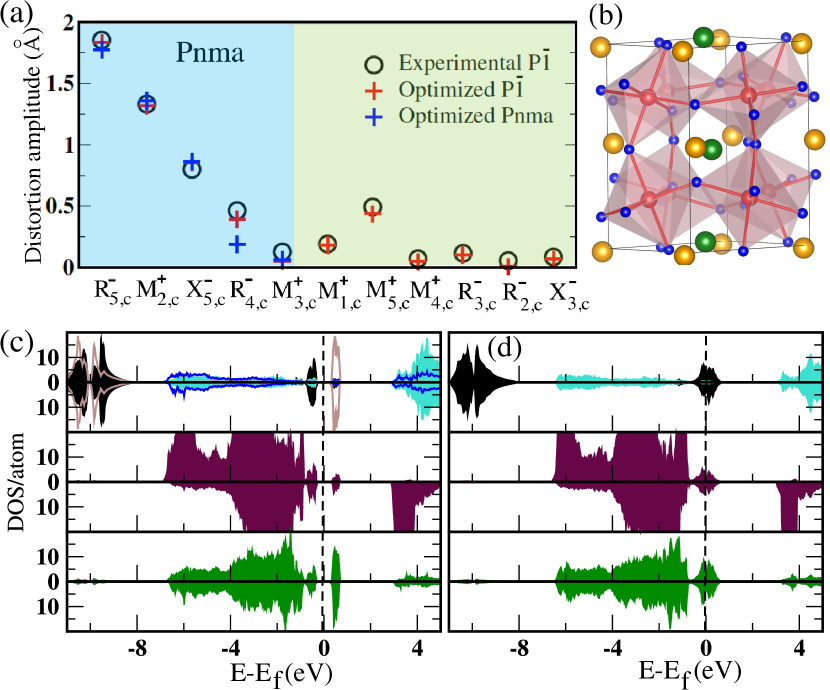
Our calculations are performed using a DFT+U approach, relying on the PBEsol [21] exchange-correlation functional, as implemented in ABINIT software[22, 23, 24] (see SI). U and J corrections are included for Ni 3 states [25]. We checked the results for different (U,J) values and found that (6,1) eV provides excellent theoretical description of the experimental ground state (see SI Table.ST1 and Fig.1(a)). For too small U, cannot be stabilized, consistently with Ref.[15]. Symmetry-adapted mode analysis is performed using Isodistort [26]. The phase to which refer each symmetry label is identified with a subscript : for cubic (m), for orthorhombic () and for monoclinic (). Connection between symmetry labels of the three phases is reported in Table.ST3. Non adiabatic charge transfer is probed using constrained DFT, as implemented in ABINIT [27].
– Starting from the experimental structure, we first carry out full structural optimization for different collinear magnetic configurations of Ni. Comparing ferromagnetic (FM) with A, C and G type antiferromagnetic (AFM) spin orders, we find G-AFM to be energetically the most favorable order (Table.ST2), with a theoretical unit cell volume (233 Å3) comparable to experiment (233-235 Å3) [14, 16]. Since G-AFM spin configuration also remains the most favorable in other phases, it is kept all along this work.
Relying on symmetry-adapted mode analysis [26], we point out in Fig.1a the excellent agreement between the optimized and experimental [28] atomic distortions of the structure, with respect to the cubic reference. Amongst these distortions, some are already inherent to the intermediate phase [29, 8]: primary in-phase () and anti-phase () NiO6 octahedra rotations together with secondary anti-polar motions of Bi atoms ( and ) and more negligible Jahn-Teller distortion (). Then, additional and distortions (Fig.S3) are also present, which explain together the lowering of symmetry from to : motions of O atoms in ab-plane, which induce a breathing-like distortion of BiO12 polyhedra and anti-phase motions of O atoms along c, which distort the polyhedra further. This gives rise to large (BiL, 51.07 Å3) and small (BiS, 47.24 Å3) Bi sites that order according to a C-type pattern in which BiL and BiS alternate along two directions and are preserved in the third one (Fig.1b). Small , and distortions are also present. The negligible contribution of the mode confirms the absence of breathing distortion at Ni sites, dominant in the insulating phase of other NiO3 perovskites [5, 8].
The partial density of states (PDOS) in Fig.1(c) reveal dominant antibonding Bi + O contributions around the Fermi energy (Ef), whereas bonding states are lying much deeper (i.e. 10 eV below Ef). In the phase, a splitting between antibonding Bi + O states is opening a band gap of 0.5 eV in line with experiment[30]. Distinct BiL and BiS contributions with occupied (unoccupied) levels near Ef are consistent with Bi3+ and Bi5+ (or Bi) states, giving rise to CO according to a C-type pattern [20]. This is confirmed by charge density plots of top valence electrons (Fig.S4a, Fig.2c), highlighting the presence of a Bi lone pairs at BiL site only. These lone pairs are pointing along the pseudo-cubic diagonal in each -plane; they are lying on the same side of Bi atoms in a given -plane and in opposite sides in consecutive layers, in line with anti-polar motion of Bi atoms and inversion symmetry of the system.
Also, PDOS of the Ni- show that states are occupied for both the spin channel and states are occupied (empty) for majority (minority) spin channel. This confirms a high-spin Ni2+() state, consistent with the calculated magnetic moment of 1.67 /Ni. Small differences in the Ni magnetic moments results in an uncompensated ferrimagnetic (FiM) net magnetization of 0.01 . Such a weak magnetisation is also observed experimentally, but as a result of a canted G-AFM ordering[28].
– The phase lies 61 meV/f.u higher in energy than . Its relaxed unit cell volume (228 Å3) is 2.4 % smaller than that of , consistently with the 2.5 % volume shrinkage observed experimentally during the transition at 3.5 GPa[16]. Structurally, the phase ( in Glazer’s notations) shows large out-of-phase and in-phase NiO6 octahedra rotations of 9.6∘ and 11.2∘, which remain similar in the phase (Fig.1a). At the electronic level, the PDOS (Fig.1d) point out a metallic character, with partially occupied Bi and O antibonding states at . The significant occupancy of Ni states and the Ni magnetic moment of 1.65 indicate a charge state closer to high-spin Ni+2 than to Ni+3, in line with experimental observations [19]. Consequently, the nominal charge state of Bi should be Bi4+, which suggests a strong tendency to electronic instability since Bi4+ is a valence skipper[31]. Accordingly, the phase shows two unstable phonon modes at : a ( 310 cm-1) and a mode (149 cm-1) that both induce CO at Bi sites.
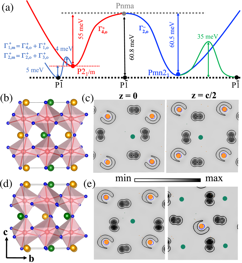
Condensing the mode lowers the symmetry to and give rise to a relaxed insulating metastable phase located 55 meV/f.u. below the phase (Fig. 2a). Inspection of the PDOS highlights a bandgap of 0.46 eV and confirms charge disproportionation at the Bi sites (Fig.-S5). This phase shows a C-type CO and lone-pair orientations similar to (Fig. 2b-c).
Condensing instead the mode lowers the symmetry to and give rise to another insultating metastable phase located 60.5 meV/f.u. below the phase (i.e. only 0.3 meV/f.u. above ). Inspection of the PDOS also show charge disproportionation at the Bi sites (shown in Fig.S5) but BiL 6s states are much broaden at the conduction level (compared to and ), indicating stronger Bi – O hybridizations resulting in a smaller bandgap of 0.3 eV. Moreover, Bi3+ and Bi5+ sites now alternate along the three directions giving rise to a G-type CO that breaks the inversion symmetry in line with the polar character of the phase.
Interestingly, the only appearance of C-type (resp. G-type) CO in already lowers the symmetry to (resp. ). Together with the close energies of , and phases, this emphasizes that the major driving force destabilizing the structure is CO, whatever the resulting order.
Path to the ground state – Amazingly the and phases are both dynamically stable. The natural path from to should preferably go through , which already condense distortion. In the monoclinic phase, none of the mode is however unstable but additional condensation of the low frequency mode (50 cm-1) properly brings the system to the ground state. Doing so requires however to overcome an energy barrier of 4 meV/f.u..
In order to clarify the mechanism of this unusual phase transition condensing a stable mode, we studied the energy landscape around the phase from a Landau-type expansion (up to 4th order) involving = and = lattice modes as well as and macroscopic strains degrees of freedom.
The expansion coefficients have been adjusted on a training set of DFT data including 300 configurations (Fig.S6 and are reported in Table ST5). Amongst the various coupling terms, we find that the 3rd order coupling is the most significant in lowering the energy (-456 meV/f.u.). Then, strain couplings (-100 meV/f.u.) and (-232 meV/f.u.) are also significant. This highlights a rather complex and unusual phase transition mechanism in which many anharmonic couplings of with , and cooperate to lower the energy and produce the ground state.
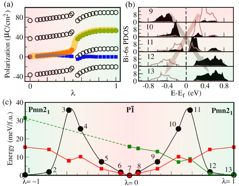
Competing polar phase and electronic ferroelectricity – Being only 0.3 meV/f.u. higher in energy than the observed ground state, the phase emerges as a close and competing phase. As previously discussed, its G-type CO (Fig.3) phase breaks inversion symmetry, yielding a spontaneous polarization along , . Further, the direction of can be reversed by reversing the charge ordering (i.e. condensing in opposite direction). Together, this makes a conceptual electronic ferroelectric phase, as long as experimental switching is practically achievable.
Estimating is not so trivial. Berry-phase calculation in the phase delivers a set of values C/cm2 (with an integer and C/cm2 the polarization quantum), without clarifying which value of is appropriate. Using a Nudged Elastic Band (NEB) technique, we identified an insulating low-energy path from non-polar to polar phase (with an energy barrier of 35 meV/f.u., Fig.2a). From this, we can follow the evolution of along the path, as illustrated in Fig.3a. This shows first that the spontaneous polarization of the phase is C/cm2, which is even larger than that of a conventional ferroelectric like BaTiO3. Then, it clarifies that the change of polarization is strongly non-linear with a jump of about 40 C/cm2. This jump that can be assigned to the change from C-type to G-type CO as highlighted from the PDOS of Bi in Fig.3b. It is also compatible (see SI) with the transfer of 2 electrons between Bi sites in one layer ( in Fig.2b) , confirming that mainly originates from electronic CO.
The non-polar character of the ground state, combined with the very close energy of the ferroelectric phase ( meV/f.u.), makes BiNiO3 a potential antiferroelectric. Applying an electric field kV/cm should be enough to stabilize thermodynamically against the phase. However, achieving electric field transition would a priori require a much larger field to overcome the adiabatic energy barrier between the two phases ( 35 meV/f.u. at zero field and zero kelvin). Alternatively, it might be questioned if non-adiabatic electron transfer would eventually be possible. Following the scheme proposed Qi and Rabe [32] (see Fig.3c and SI), we estimate the field required for non-adiabatic transition to kV/cm ( meV/f.u.). As discussed by Qi and Rabe, this should not be taken as an exact value but rather as an estimate to compare distinct compounds. Our computed is larger than that in Fe3O4 [32] showing a similar bandgap and in which ferroelectric switching has been experimentally observed [33]. It is however significantly smaller than in other electronic ferroelectrics like SrVO3/LaVO3 or LuFe2O4 [32]. As such, BiNiO3 remains a plausible candidate for electronic antiferroelectricity, with field induced non-polar to polar transition potentially accessible and driven by non-adiabatic electron transfer.
Strain engineering – Interestingly, the lattice parameters (along a and c) of the phase are significantly different from those of the ground state (see Table.-ST7), which opens the perspective of using strain engineering to stabilize a ferroelectric ground state. It appears that the lattice parameters of the NdGaO3, a widely used substrate for the growth of perovskite oxide films, perfectly match with those of the phase. Comparing then the energies of different possible orientations of and phases, epitaxially strained on commercially available (110)o and (001)o NdGaO3 substrates (Table.ST8,ST9), it appears that the ferroelectric phase is always elastically favored. In the case of the (110)o substrate, the strained ferroelectric phase lies 7 meV/f.u. below the strained and moreover aligns its long axis in plane as that of the substrate, which makes it a likely case to be realized experimentally. Polarization switching in such a marginally strained polar phase would require reversing the CO and as such electron transfer in each of the two layers ( and of Fig.2d). According to Fig.3c, it should be accessible from non-adiabatic electron transfer at the same reasonable field kV/cm as before, making the system a potential electronic ferroelectric.
Conclusions – BiNiO3 behaves differently than other nickelate perovskites, which show CO at Ni sites. The charge transfer , yielding the valence skipper state, is the starting point for the electronic instability of the metallic phase, which is then further stabilized by CO at Bi sites in the insulating non-polar ground state and close feroelectric phase. TlMnO3[35] is another alternative perovskite we found hosting a ground state. Interestingly, it also shows a metallic to insulating phase transition but coming instead from orbital ordering at Mn3+ sites. We want to stress that ferroelectricity in BiNiO3 is distinct from that in other BiO3 perovskites (= Fe, Co, In) [36, 37, 38] in which only Bi3+ is present and polarisation driven by the lone pair of Bi3+. In BiNiO3, the polarisation arises from the G-type Bi3+/Bi5+ CO and is electronic in nature. Electronic ferroelectricty has been reported in non-perovskite Fe3O4[33], Fe2O4 compounds [39, 40] and perovskite oxide superlattices [41, 42] but remains a rare phenomena. Stabilizing the polar phase of BiNiO3 by electric field or strain enginering appears as a promising new platform to probe further the intriguing concept of electronic (anti-)ferroelectricity.
SB thanks He Xu for useful discussions and technical support. This work was supported by F.R.S.-FNRS Belgium under PDR grant T.0107.20 (PROMOSPAN). The authors acknowledge the use of the CECI supercomputer facilities funded by the F.R.S-FNRS (Grant No. 2.5020.1) and of the Tier-1 supercomputer of the Fédération Wallonie-Bruxelles funded by the Walloon Region (Grant No. 1117545).
References
- Zhou et al. [2016] Y. Zhou, X. Guan, H. Zhou, K. Ramadoss, S. Adam, H. Liu, S. Lee, J. Shi, M. Tsuchiya, D. D. Fong, and S. Ramanathan, Nature 534, 231 (2016).
- Shi et al. [2013] J. Shi, S. D. Ha, Y. Zhou, F. Schoofs, and S. Ramanathan, Nature Communications 4, 2676 (2013).
- Alonso et al. [1999] J. A. Alonso, M. J. Martínez-Lope, M. T. Casais, M. A. G. Aranda, and M. T. Fernández-Díaz, Journal of the American Chemical Society 121, 4754 (1999), https://doi.org/10.1021/ja984015x .
- Mazin et al. [2007] I. I. Mazin, D. I. Khomskii, R. Lengsdorf, J. A. Alonso, W. G. Marshall, R. M. Ibberson, A. Podlesnyak, M. J. Martínez-Lope, and M. M. Abd-Elmeguid, Phys. Rev. Lett. 98, 176406 (2007).
- Varignon et al. [2017a] J. Varignon, M. N. Grisolia, J. Íñiguez, A. Barthélémy, and M. Bibes, npj Quantum Materials 2, 21 (2017a).
- Johnston et al. [2014] S. Johnston, A. Mukherjee, I. Elfimov, M. Berciu, and G. A. Sawatzky, Phys. Rev. Lett. 112, 106404 (2014).
- Bisogni et al. [2016] V. Bisogni, S. Catalano, R. J. Green, M. Gibert, R. Scherwitzl, Y. Huang, V. N. Strocov, P. Zubko, S. Balandeh, J.-M. Triscone, G. Sawatzky, and T. Schmitt, Nature Communications 7, 13017 (2016).
- Mercy et al. [2017] A. Mercy, J. Bieder, J. Íñiguez, and P. Ghosez, Nature Communications 8, 1677 (2017).
- Shannon [1976] R. D. Shannon, Acta Crystallographica Section A 32, 751 (1976).
- [10] M. Lufaso, https://www.unf.edu/ michael.lufaso/spuds/radii-alpha.pdf .
- Brese and O’Keeffe [1991] N. E. Brese and M. O’Keeffe, Acta Crystallographica Section B 47, 192 (1991).
- Goldschmidt [1926] V. M. Goldschmidt, Naturwissenschaften 14, 477 (1926).
- Ishiwata et al. [2002a] S. Ishiwata, M. Azuma, M. Takano, E. Nishibori, M. Takata, M. Sakata, and K. Kato, J. Mater. Chem. 12, 3733 (2002a).
- Azuma et al. [2007] M. Azuma, S. Carlsson, J. Rodgers, M. G. Tucker, M. Tsujimoto, S. Ishiwata, S. Isoda, Y. Shimakawa, M. Takano, and J. P. Attfield, Journal of the American Chemical Society 129, 14433 (2007).
- Cohen and Diéguez [2021] N. Cohen and O. Diéguez, Phys. Rev. B 104, 064111 (2021).
- Azuma et al. [2011] M. Azuma, W.-t. Chen, H. Seki, M. Czapski, S. Olga, K. Oka, M. Mizumaki, T. Watanuki, N. Ishimatsu, N. Kawamura, S. Ishiwata, M. G. Tucker, Y. Shimakawa, and J. P. Attfield, Nature Communications 2, 347 (2011).
- Naka et al. [2016] M. Naka, H. Seo, and Y. Motome, Phys. Rev. Lett. 116, 056402 (2016).
- Kojima et al. [2016] S. Kojima, J. Nasu, and A. Koga, Phys. Rev. B 94, 045103 (2016).
- Mizumaki et al. [2009] M. Mizumaki, N. Ishimatsu, N. Kawamura, M. Azuma, Y. Shimakawa, M. Takano, and T. Uozumi, Phys. Rev. B 80, 233104 (2009).
- Paul et al. [2019] A. Paul, A. Mukherjee, I. Dasgupta, A. Paramekanti, and T. Saha-Dasgupta, Phys. Rev. Lett. 122, 016404 (2019).
- Perdew et al. [2008] J. P. Perdew, A. Ruzsinszky, G. I. Csonka, O. A. Vydrov, G. E. Scuseria, L. A. Constantin, X. Zhou, and K. Burke, Phys. Rev. Lett. 100, 136406 (2008).
- Gonze et al. [2002] X. Gonze, J.-M. Beuken, R. Caracas, F. Detraux, M. Fuchs, G.-M. Rignanese, L. Sindic, M. Verstraete, G. Zerah, F. Jollet, M. Torrent, A. Roy, M. Mikami, P. Ghosez, J.-Y. Raty, and D. Allan, Computational Materials Science 25, 478 (2002).
- Gonze [2005] X. Gonze, Zeitschrift für Kristallographie - Crystalline Materials 220, 558 (2005).
- Torrent et al. [2008] M. Torrent, F. Jollet, F. Bottin, G. Zérah, and X. Gonze, Computational Materials Science 42, 337 (2008).
- Liechtenstein et al. [1995] A. I. Liechtenstein, V. I. Anisimov, and J. Zaanen, Phys. Rev. B 52, R5467 (1995).
- [26] H. T. Stokes, D. M. Hatch, and B. J. Campbell, ISOTROPY Software Suite .
- Gonze et al. [2022] X. Gonze, B. Seddon, J. A. Elliott, C. Tantardini, and A. V. Shapeev, Journal of Chemical Theory and Computation 18, 6099 (2022), pMID: 36099643, https://doi.org/10.1021/acs.jctc.2c00673 .
- Carlsson et al. [2008] S. J. Carlsson, M. Azuma, Y. Shimakawa, M. Takano, A. Hewat, and J. P. Attfield, Journal of Solid State Chemistry 181, 611 (2008).
- Varignon et al. [2017b] J. Varignon, M. N. Grisolia, D. Preziosi, P. Ghosez, and M. Bibes, Phys. Rev. B 96, 235106 (2017b).
- Ishiwata et al. [2002b] S. Ishiwata, M. Azuma, M. Takano, E. Nishibori, M. Takata, M. Sakata, and K. Kato, J. Mater. Chem. 12, 3733 (2002b).
- Varma [1988] C. M. Varma, Phys. Rev. Lett. 61, 2713 (1988).
- Qi and Rabe [2022] Y. Qi and K. M. Rabe, Phys. Rev. B 106, 125131 (2022).
- Yamauchi et al. [2009] K. Yamauchi, T. Fukushima, and S. Picozzi, Phys. Rev. B 79, 212404 (2009).
- [34] Non-adiabatic paths have been obtained fixing the atomic geometry to or and then constraining the electronic charge at each point to what it is along the adiabatic path, using constrained- calculations.
- Yi et al. [2014] W. Yi, Y. Kumagai, N. A. Spaldin, Y. Matsushita, A. Sato, I. A. Presniakov, A. V. Sobolev, Y. S. Glazkova, and A. A. Belik, Inorganic Chemistry 53, 9800 (2014).
- Neaton et al. [2005] J. B. Neaton, C. Ederer, U. V. Waghmare, N. A. Spaldin, and K. M. Rabe, Phys. Rev. B 71, 014113 (2005).
- Oka et al. [2010] K. Oka, M. Azuma, W.-t. Chen, H. Yusa, A. A. Belik, E. Takayama-Muromachi, M. Mizumaki, N. Ishimatsu, N. Hiraoka, M. Tsujimoto, M. G. Tucker, J. P. Attfield, and Y. Shimakawa, Journal of the American Chemical Society 132, 9438 (2010), pMID: 20568754.
- Belik et al. [2006] A. A. Belik, S. Y. Stefanovich, B. I. Lazoryak, and E. Takayama-Muromachi, Chemistry of Materials 18, 1964 (2006), https://doi.org/10.1021/cm052627s .
- Ikeda et al. [2005] N. Ikeda, H. Ohsumi, K. Ohwada, K. Ishii, T. Inami, K. Kakurai, Y. Murakami, K. Yoshii, S. Mori, Y. Horibe, and H. Kitô, Nature 436, 1136 (2005).
- Fujiwara et al. [2021] K. Fujiwara, Y. Fukada, Y. Okuda, R. Seimiya, N. Ikeda, K. Yokoyama, H. Yu, S. Koshihara, and Y. Okimoto, Scientific Reports 11, 4277 (2021).
- Park et al. [2019] S. Y. Park, K. M. Rabe, and J. B. Neaton, Proceedings of the National Academy of Sciences 116, 23972 (2019).
- Park et al. [2017] S. Y. Park, A. Kumar, and K. M. Rabe, Physical Review Letters 118, 087602 (2017).