WWW: What, When, Where to Compute-in-Memory
Abstract
Compute-in-memory (CiM) has emerged as a compelling solution to alleviate high data movement costs in von Neumann machines. CiM can perform massively parallel general matrix multiplication (GEMM) operations in memory, the dominant computation in Machine Learning (ML) inference.
However, re-purposing memory for compute poses key questions on 1) What type of CiM to use: Given a multitude of analog and digital CiMs, determining their suitability from systems perspective is needed. 2) When to use CiM: ML inference includes workloads with a variety of memory and compute requirements, making it difficult to identify when CiM is more beneficial than standard processing cores. 3) Where to integrate CiM: Each memory level has different bandwidth and capacity, that affects the data movement and locality benefits of CiM integration.
In this paper, we explore answers to these questions regarding CiM integration for ML inference acceleration. We use Timeloop-Accelergy [1, 2] for early system-level evaluation of CiM prototypes, including both analog and digital primitives. We integrate CiM into different cache memory levels in an Nvidia A100-like baseline architecture and tailor the dataflow for various ML workloads. Our experiments show CiM architectures improve energy efficiency, achieving up to 0.12x lower energy than the established baseline with INT-8 precision, and upto 4x performance gains with weight interleaving and duplication. The proposed work provides insights into what type of CiM to use, and when and where to optimally integrate it in the cache hierarchy for GEMM acceleration.
Index Terms:
compute-in-memory, SRAM, GEMMs, memory hierarchy, machine learning inference, hybrid architecturesI Introduction
Machine learning (ML) applications have become ubiquitous across various domains such as automotive, health care, finance, and technology. This has led to an increase in demand for high-performance and energy-efficient ML hardware solutions.
Matrix-vector multiplications and general matrix-matrix multiplications, known as GEMMs, are at the core of ML workloads such as convolutional networks and transformers[3, 4].
Due to the data intensive nature of such computations, they could incur high energy costs, particularly in von Neumann architectures such as Central Processing Units (CPUs) and Graphics Processing Units (GPUs). Such high energy costs are attributed to the separation of processing units from memory in such architectures among others, resulting in costly memory accesses and data movements between the processing unit and memory, commonly known as the “memory wall” or “von-Neumann bottleneck”
[5]. To address this, Compute-in-Memory (CiM) paradigms have been proposed to reduce the expensive data movement costs and provide energy-efficient solutions by performing computations in the memory [6, 7].
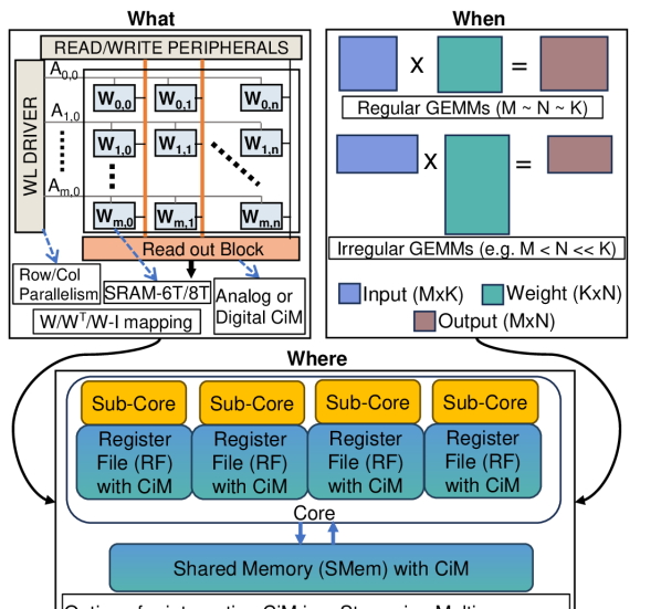
There are numerous ways of integrating CiM across the memory hierarchy: from CMOS on-chip cache memory to DRAM or Flash [8, 9, 10]. In this work, we focus on adding CiM in on-chip memory subsystem, as it does not require radical technological changes. While integrating CiM in caches has been explored [11, 12, 13], a comprehensive evaluation for effectiveness of different types of CiM primitives (or designs) at the system level, particularly for ML inference, is yet to be studied. Our work explores the benefits of integrating CiM to different cache levels, Register File (RF) and Shared Memory (SMem), in a Streaming Multiprocessor (SM) of a GPU (Fig. 1). GPUs consist of hundreds of SMs which are connected through large crossbar interconnect to DRAM via L2 memory [14]. To efficiently utilize CiM in a memory subsystem, there is a need to determine the optimum type of CiM, when to use it, and where to use it, for ML inference.
What type of CiM: CiM can be broadly classified as analog or digital based on their nature of computing [15, 16, 17, 18, 19, 20, 21]. Analog CiM performs multiply and accumulate (MAC) operations in the analog/mixed signal domain inside a memory array. For communications among different CiM blocks, peripheral circuits such as Digital-to-Analog (DAC) and Analog-to-Digital (ADC) converters are required to reduce the impact of analog noise on computation. ADCs usually have high area, latency and energy costs, increasing the overhead of analog CiM. In contrast, digital CiM performs all the computations in the digital domain by performing bit-wise AND/XOR or multiply operations. To calculate the final MAC output, multiple bit-wise operations are performed that can increase the compute latency for Digital CiM. Also, design choices such as the type of memory cell (SRAM-6T/8T), the number of wordlines or bitlines enabled at a time, and the mapping scheme for weights in the memory array have made it increasingly challenging to identify the most effective CiM primitive in a system.
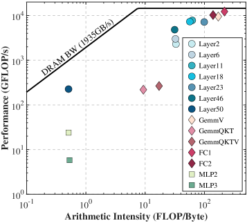
When to use CiM: ML models consist of a variety of GEMM shapes and sizes. GEMM () computation can be thought of as multiplying input matrix of size with weight matrix of size to get an output matrix of size [22]. Arithmetic intensity, or data reuse, gives an idea of the dependence of GEMM computations on memory, by calculating the ratio of arithmetic operations (Floating Point Operations or FLOPs) to memory accesses (bytes). A roofline representation of performance versus arithmetic intensity for GEMMs is shown in Fig. 2. The graph demonstrates that 1) not all GEMMs require the full capabilities of the GPUs, resulting in under-utilization of SM. CiM has the potential to maintain performance comparable to standard computing paradigms, when adopted for GEMM computations. 2) GEMMs have a wide range of compute and memory requirements. Hence, it is not clear when those energy and performance benefits of CiM would be higher than the baseline.
Where to integrate CiM: Since GEMMs have regular data access patterns and offer high temporal and spatial locality, the matrices are fetched from main memory to caches in blocks or smaller tiles [23]. Typically, GPUs optimize their memory hierarchy to efficiently reuse the tile data and parallelize GEMM operations across hundreds of tensor cores present in sub-cores of SMs. CiM based hardware designs are also capable of performing parallel matrix multiplications by enabling multiple columns and rows inside a memory array and leveraging parallelism from multiple memory arrays. However, each memory level differs in terms of bandwidth and storage capacity (Table V), which affects the data reuse opportunities and compute parallelism when re-purposed with CiM features. Hence, it is crucial to find if there is a memory level that can exploit the locality well and provide highest CIM benefits.
Our approach: To fully leverage and evaluate the benefits of CiM compared to general-purpose processors, we consider a range of workload specifications, memory levels and CiM characteristics. Subsequently, choosing optimal dataflow for given specifications is important to achieve highest possible performance and energy efficiency. Optimal dataflow affects the data reuse by reducing the number of memory accesses through efficient scheduling and allocation of GEMMs on given hardware resources. While Algorithmic data reuse for GEMMs can be calculated as the number of MAC operations divided by the total size of matrices. Note however, the observed data reuse is determined by the dataflow because it is dependent on the actual number of memory accesses.
The main contributions of the work can be summarized as follows:
-
•
An analytical evaluation of SRAM-based analog and digital CiM primitives at RF and SMem levels in an Nvidia-A100 like baseline architecture.
-
•
Optimizing the performance and energy efficiency gains from CiM by finding optimal dataflow for a given CiM architecture and GEMM shape.
-
•
Detailed answers to the questions on what, when and where to CiM for various GEMM shapes from energy/performance perspective.
The rest of the paper is organized as follows: Section II distinguishes our work from other studies done in the past. The next section (III) provides relevant background for this work. Section IV describes details of the set of CiM primitives used for the experiments.
The following section (V) highlights the key takeaways along with results and discussions, followed by conclusion in the last section.
II Related Works
While there has been work considering in-cache computing in CPUs, there have not been studies re-purposing GPU memory for compute. For example, Duality cache [11] architecture re-purposes last level cache in Server class Xeon processors to accelerate data parallel applications. They also extend the system stack to develop a CUDA like Single Instruction Multiple Thread (SIMT) programming model for executing floating point and integer arithmetic operations in cache. MLIMP [12] extends the concept of Duality Cache for graph neural networks, by developing a concurrent task scheduler for multi-layer in-memory processing systems. They propose job scheduling and memory allocation algorithms based on the memory type (bit-serial in-memory/in-ReRAM/in-DRAM). On the other hand, this work focuses on analyzing the benefits of re-purposing different levels in the memory hierarchy of a GPU for ML inference. We consider GPUs because of their widespread dominance in accelerating GEMMs, the core computation in inference tasks. In addition, GPUs are programmable accelerators and the same programming model could be potentially re-used for CiM integrated GPUs.
Livia [13] also looked at modifying cache memory in CPUs to minimize overall data movement for irregular data access applications. It proposes a system architecture that dynamically schedules tasks and data at different locations in the memory hierarchy. In contrast, we focus on highly regular workloads (GEMMs) and determining if the parallelism offered by CiM primitives can match the locality benefits offered by cache hierarchy.
To-Pim-or-Not [25] is the first work to raise the questions on how, and when to use processing-in-memory (PIM) for different applications. It focuses on the development of a software framework to determine when and how to effectively offload computations to PIM while analyzing the trade-offs between performance benefits and offload costs. However, the scope of the work is limited to emerging general purpose DDR Memory Systems, creating a gap in the understanding of SRAM based CIM primitives. Our work fills this gap by considering CiM in cache hierarchy for general purpose GPUs. Another recent work [26] on benchmarking analog vs. digital compute in memory develops a quantitative energy model based on fixed analog CiM and digital CiM designs, referred to as templates. However, CiM macros vary significantly in terms of the peripheral circuits and using a template limits the design options for CiM primitive macros. Moreover, it does not mention about CiM latency or performance estimation in a system with configurable dataflow options. We leverage the Timeloop model [1] methodology to perform an analytical evaluation of a system for different CiM primitives. Timeloop considers a generic architecture template with arithmetic units and a memory hierarchy.
III Background
III-A Importance of GEMMs in ML Workloads
Machine learning workloads consist of a broad range of neural networks from convolutional, fully connected, to transformer and recommendation models. Matrix-vector multiplication and matrix-matrix multiplications are at the core of computation in these neural networks [3, 4]. In this work, we refer to such multiplications under one umbrella term, known as general matrix-matrix multiplications or GEMMs (). , and are used to represent the dimension of matrices (Fig. 1), where is the reduction dimension.
Convolution neural networks (CNNs) can be implemented as GEMMs by transforming the convolution operation of input and weight feature maps to matrix-matrix multiplication using im2col [22]. im2col or image-to-column transformation converts the 3D convolution operation to a GEMM () such that represents the reduction dimension for the MAC operation between inputs and weights, represents the total number of such reductions or convolutions and is decided based on the number of output channels. The initial layers of a CNN generally have larger input feature maps compared to other layers, for larger datasets such as ImageNet. The last layer is a classifier, which is essentially a fully connected (FC) layer. It consists of matrix vector multiplications, which can be thought of as a special case of GEMM. Similarly, transformer models perform computation of the Query (), Key (), and Value () matrices from input embedding in the initial layers, which can be visualized as same shaped GEMMs. Additionally, transformer models comprise of other GEMMs such as logit (), attention (), and output () calculations, followed by FC layers. On the other hand, recommendation models incorporate multilayer perceptrons (MLPs) to predict items from a pool of dense features and user preferences [27], basically consisting of FC layers. GEMM shapes, representing a range of shapes and sizes from various ML workloads, are listed in Table I.
| Model name | Layer | M | N | K | #MACs | Data Reuse |
|---|---|---|---|---|---|---|
| ResNet50 | Layer2 | 3136 | 64 | 64 | 12845056 | 63.35 |
| Layer6 | 3136 | 64 | 576 | 115605504 | 113.12 | |
| Layer11 | 3136 | 128 | 256 | 102760448 | 166.15 | |
| Layer18 | 784 | 128 | 1152 | 115605504 | 200.88 | |
| Layer23 | 784 | 256 | 512 | 102760448 | 280.31 | |
| Layer46 | 49 | 2048 | 512 | 51380224 | 87.53 | |
| Layer50 | 1 | 1000 | 2048 | 2048000 | 2.00 | |
| BERT | GemmV | 512 | 1024 | 1024 | 536870912 | 512.00 |
| GemmQKT | 32 | 32 | 1024 | 1048576 | 31.51 | |
| GemmQKTV | 32 | 1024 | 32 | 1048576 | 31.51 | |
| FC1 | 512 | 4096 | 1024 | 2147483648 | 630.15 | |
| FC2 | 512 | 1024 | 4096 | 2147483648 | 630.15 | |
| DLRM | MLP2 | 1 | 256 | 512 | 131072 | 1.99 |
| MLP3 | 1 | 64 | 256 | 16384 | 1.96 |
III-B SRAM based Compute-in-Memory Primitives
Given the high cost of memory accesses compared to logic operations [28], many works have been proposed to perform computations in on-chip SRAM [29]. These CiM macros can be designed in various ways based
– analog or digital. Another key factor is the type of SRAM cells used. These cells vary in their transistor counts, with common examples including 6T [20], 8T [17], and 10T [30] cells. Additionally, CiM macros vary in the way input data are stored or applied to CiM compute. For instance, input can be stored in the CiM macro itself or it can be applied to the CiM macro from an external buffer.
In digital CiM, the multiply and accumulate operations are performed in the digital domain through bit-serial logic gates. A sequence of such logic operations can be then combined to perform arithmetic operations. Such logic is usually placed in the peripheral circuitry of the CiM macro [15, 18, 19]. The degree of compute parallelism in digital CiM macros generally depends on the amount of logic resources added in the macro. However, adding more logic circuits to digital CiM designs leads to significant area overhead [18], resulting in performance/energy – area trade-off. On the other hand, analog CiM macros perform MAC operations by applying input bits through wordlines while storing the weights in the CiM macro [16, 17]. The output is produced as an analog voltage or current at the bitlines, which needs to be converted to digital through an Analog to Digital Converter (ADC) for robust inter-macro communication. Notably, ADCs are the major area/latency/energy bottlenecks in analog CiM macros [31]. Prior art tried to amortize the cost of ADCs for better energy-efficiency/performance through narrower output precision or novel ADC circuit designs [16, 17]. It is worth mentioning that digital CiM scales with the most advanced technology nodes [19] unlike analog CiM where ADCs suffer from significant noise at such advanced technology nodes [32].
As mentioned before, CiM macros comprise various SRAM cell types. 8T-cells are commonly adopted in CiM macros since they have decoupled read and write ports, leading to minimal read-disturb issues [15] and higher noise margin than 6T cells. 8T-based CiMs enable multiple wordlines simultaneously leading to more parallel MAC operations and energy efficiency. On the other hand, 6T-cells are the de-facto standard for conventional SRAM designs due their compact area. 6T-based CiM have been proposed to reduce the area overhead of 8T cells. To avoid the read disturb issue in 6T-based CiM macros, several circuit techniques have been proposed [16, 20, 18]. For example, to perform 6T-based analog CiM, [16, 20] added a local computing block to a group of 6T cells that share the same bitline. There are multiple groups in a column where two cells from different groups do not share the same bitline. Note, only one 6T cell is activated per local computing group during computation to avoid read disturb. In addition to 6T and 8T based CiM, some reported macros adopted other cell types (e.g. 10T [30]) that can perform more complex computations (such as in-memory addition and membrane potential updates for spiking neural networks) within the cell while leading to larger area overhead.
CiM macros also vary in the way inputs are applied. Input data can be stored in the CiM macro itself prior computations [15], or streamed in the macro during the CiM operation from an external buffer [17]. Input storing/streaming imposes different mapping/dataflow constraints on the corresponding CiM macro leading to different optimal data orchestration.
Additionally, various input/output precisions have been shown in such works leading to comparisons challenges. To have a fair comparison, we fix input/output precision to 8-bit integer in this work. It is also worth mentioning that different CiM macros might impose certain dataflows at the macro level due to their unique compute nature [15, 16].
III-C Dataflow Optimization in Cache Hierarchy
GEMMs exhibit high spatial and temporal locality owing to their regular data access patterns. To exploit this locality, GPUs implement GEMMs by tiling (or blocking) the output matrix, and performing tile computations in parallel [23]. For a given dataflow, loop factor explains the size of such tiles and loop order (order of in loop representation of dataflow) decides the reuse of tile at a given memory level. Algorithmically, arithmetic intensity or data reuse can be calculated as number of operations divided by the total size of matrices fetched from the memory:
| (1) |
assuming each matrix is accessed once from the main memory, where BP is the bit-precision.
The number of memory accesses is decided by how the matrices are divided into tiles and the order of fetching the different matrix dimension, referred as dataflow. Hence, observed data reuse could be different than algorithmic data reuse.
The performance of GEMMs is limited by their algorithmic arithmetic intensity and the hardware resources. Low arithmetic intensity GEMMs are limited by the memory bandwidth, while high arithmetic intensity GEMMs are limited by the peak performance. Libraries such as cuDNN and cuBLAS are used to decide the tile sizes for achieving highest possible performance for given GEMM shape. Larger tiles often lead to greater data reuse. This increase in data reuse can result in lower bandwidth requirements and improved efficiency. However, opting for larger tiles could reduce the number of tiles that can run in parallel. This reduction can potentially lead to lower performance.
Given that the implementation of GEMMs is optimized on GPUs to get the best performance, it is important to realize the best dataflow for CiM intergrated architecture as well. There are several studies for exploring the dataflow search space and choosing the optimal dataflow. SCNN [33] was one of the first works which introduced dataflow optimization for deep neural networks (DNNs). They proposed an input-stationary dataflow, where input activation is held stationary, allowing it to be multiplied by all the filter weights necessary for each output channel. Further, Timeloop [1] presented a low cost mapper and model to explore dataflow search space for DNNs and GEMMs. It models the input problem size as a nested loop, allowing for the assessment of data reuse opportunities and efficient mapping across different architectures and workloads. Maestro [34] is another tool that proposes an analytical cost model to assesses the cost-benefit tradeoffs in dataflow using their data centric approach. ZigZag [35] also explores the DNN accelerator design space by expanding the search to uneven scheduling opportunities.
IV CiM Architecture Construction
To get an estimate of energy and performance of different CiM primitives, all the evaluations are done using Timeloop-Accelergy framework[1]. We choose Timeloop/Accelergy infrastructure because 1. it is a fast analytical model that is used widely in research projects for early design estimations, 2. it provides a mapper to chose the optimal dataflow for a given architecture, and 3. it is a flexible tool, used to model analog CiM in the past[36].
| Parameter | Description |
|---|---|
| Rp | Row parallelism or number of rows turned on in an array |
| Cp | Column parallelism or number of columns turned on in an array |
| n | Number of weight (and/or input) elements stored in each CiM unit |
| Storage size | Capacity of each CiM Unit (may include memory cells used for reduction) |
| MeshX | Number of CiM arrays in X dimension |
| MeshY | Number of CiM arrays in Y dimension |
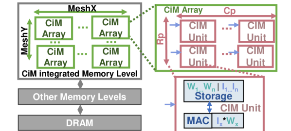
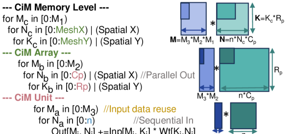
The framework takes architecture, constraint, mapper configuration and energy table files as inputs. For our evaluation, separate architecture template files are created for integrating CiM at RF and SMem levels (Fig. 1). As shown in Fig. 3, such an architecture template replaces the arithmetic block with memory level re-purposed into CiM. Such CiM integrated memory level consists of multiple CiM arrays (, ) dependent on the memory size and capacity. Each CiM array is a network of CiM units, which can compute one MAC at a time. The number of CiM units is decided by the number of rows () and columns () turned on simultaneously in an array. All CiM units can, thus, perform MAC operations in parallel. Since all columns/rows are not generally turned on simultaneously in a CiM array, this sequential nature of CiM array is incorporated in the form of a temporal loop factor () (refer Figure 6). n decides the size of the storage component associated with each CiM unit to represent the sequential behaviour in dataflow representation. Such parallel out - sequential in template approach (Fig. 3) captures both analog and digital based CiM types. The detailed list of parameters used in CiM architecture template is described in Table II.
A CiM energy table is provided to Accelergy based on the measured performance numbers from the original CiM silicon prototypes. Since the prototypes differ in terms of supply voltage and technology, the energy numbers are scaled to match 32nm technology with 1V supply according to the established work on scaling [37]. The difference in frequency of operation of the CiM primitives is captured through compute cycles in terms of latency, by assuming 1GHz frequency in Timeloop architecture template. Constraint configuration is adjusted to get the optimum dataflow for each input specification, as described in the next section.
V Evaluation
V-A Experimental Setup
V-A1 Cim Primitives
| Attributes | CiM Primitive | |||
|---|---|---|---|---|
| Analog-1 | Analog-2 | Digital-1 | Digital-2 | |
| 8b-8b MAC Energy (pJ) | 0.14 | 0.17 | 0.64 | 0.82 |
| Compute Latency (ns) | 9 | 144 | 18 | 233 |
| Area increase (x) | 1.34 | 2.17 | 1.4 | 1.1 |
| n (temporal loop) | 16 | 16 | 1 | 10 |
| CiM Unit Storage (B) | 16 | 16 | 1 | 32 |
| (Rp, Cp) | (4,64) | (64,4) | (256,32) | (1,128) |
| CiM Array size (rows x col) | 512x64 | 64x512 | 256x256 | 256x128 |
| Mapping (Stationarity) | Weight | Weight | Weight | Weight-Input |
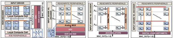
We have chosen two state-of-the-art SRAM-based primitives for both analog/mixed-signal and digital CiM, as shown in Fig. 4. These primitives cover a range of distinct and varying parameters, as listed in Table III and explained below.
The Analog-1 [16] CiM primitive, illustrated in Fig. 4(a), consists of 4 banks, each with 4 blocks of 128x64 SRAM6T cells. It employs a transpose mapping technique, feeding inputs to multiple columns. This configuration results in 256 (464) CiM units, each with 128b (168b) storage. Each unit can perform an 8b-8b MAC operation in 9 cycles, processing 2b inputs and activating 8 rows of weight bits simultaneously. However, due to the limited number of ADCs shared per bank, the temporal loop factor for this primitive is set at 16.
The Analog-2[17] primitive, depicted in Fig. 4(b), features a re-configurable ADC design with 8 arrays, each array (6464) storing a different bit of weight and having 4 ADC outputs per compute cycle. This design results in 256 (644) CiM units, each capable of performing 8b-8b MAC in 144 cycles, including bit-serial latency and scaling adjustments from 65nm to 32nm. Each CiM unit contains 8(644) weight bits which are computed in sequence due to ADC limitation. This primitive has lower energy per compute but suffers from higher area overhead due to the re-configurable nature.
The Digital-1[18], shown in Fig. 4(c), employs a fully digital design, feeding inputs into each row and executing a MAC operation at every column using an adder tree. Here, each CiM unit computes 1 8b-8b MAC by combining weight bits stored in 8 columns. The adder tree reduction incurs an area overhead and results in a compute latency of 18 cycles.
The Digital-2[15] primitive, in Fig. 4(d), shows a design where both inputs and weights are mapped to the same column. This configuration allows each CiM unit, comprising a single column, to perform approximately 10 8b-8b MAC operations. However, each operation requires 233 cycles, attributed to multiple additions involved in the process. Despite a small area overhead, the compute parallelism is limited here due to the allocation of some array bits in a column for output reduction.
V-A2 GEMM shapes
We characterized a variety of GEMM shapes from commonly used ML models such as ResNet50 [38] with ImageNet [39], BERT-medium [40] with sequence length equal to 1024 and DLRM [27]. We pruned the GEMM shapes based on their unique properties as listed in Table IV to cover different weight sizes, shapes and compute nature. Compute intensive GEMMs lie below the flat roof in roofline representation as shown in Fig. 2. Their data reuse is higher, implying the number of computations done per memory access is high. On the other hand, memory intensive GEMMs lie below the bandwidth bound roof, dominated by memory accesses rather than computations. The less compute intensive GEMMs in the table technically fall in the compute intensive region. However, they have medium data reuse with skewed shapes.
| Model name | Layer | Type | Attributes |
|---|---|---|---|
| ResNet50 | Layer2 | Compute intensive | , Small weight |
| Layer6 | Compute intensive | , Small weight | |
| Layer11 | Compute intensive | , Medium weight | |
| Layer18 | Compute intensive | , Large weight | |
| Layer23 | Compute intensive | , Large weight | |
| Layer46 | Compute intensive | , Large weight | |
| Layer50 | Memory intensive | , Large weight | |
| BERT | GemmV | Compute intensive | , Large weight |
| GemmQKT | Less Compute intensive | , Medium weight | |
| GemmQKTV | Less Compute intensive | , Medium weight | |
| FC1 | Compute intensive | , Largest weight | |
| FC2 | Compute intensive | , Largest weight | |
| DLRM | MLP2 | Memory intensive | , Medium weight |
| MLP3 | Memory intensive | , Small weight |
V-A3 Baseline
We assume a single SM baseline architecture, consistent with the specifications of one of the latest GPUs (Nvidia A100), as detailed in Table V. All experiments are conducted under INT-8 precision, weight stationary dataflow and iso-area constraints using Timeloop/Accelergy framework. INT-8 is chosen for its acceptable accuracy in ML inference tasks[41, 42]. Iso-area assumes that the memory level area remains the same after CiM integration by adjusting the capacity. Since A100 consists of 108 SMs, we approximately assume 10% of the total HBM bandwidth for 1 SM architecture.
V-B Impact of Dataflow
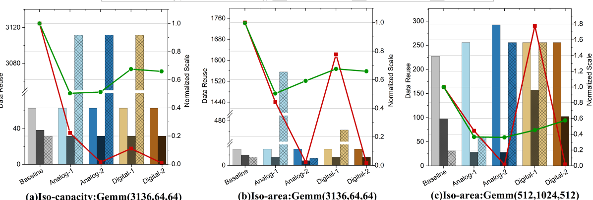
In this sub-section, we briefly discuss two GEMM shapes with CiM integrated at RF to highlight how the different primitives leverage data reuse opportunities. Optimal dataflow is found using Timeloop mapper by setting the constraint file for each primitive. A sample dataflow at the CiM level is shown in Fig. 5 where highlighted parameters are set in the constraint file based on the CiM type. To maximise performance, we set the constraints for mapping such that maximum computations are done in parallel in CiM units, i.e., using weight interleaving. Other priorities are to maximize input data reuse for mapped weights and allowing weight duplication when beneficial.
For the case when the weight () matrix is small and M significantly exceeds and (in Fig. 5(a) Gemm-), weight can fit in the CiM integrated RF memory. Here, each CiM primitive consists of 4096 CiM units. The baseline already achieves the highest data reuse (63, see Table I) at DRAM and it is maintained across CiM primitives. However, CiM can better exploit input data reuse (3112) at RF level by reusing the whole input tile () stored at SMem. This results in lower number of memory accesses with CiM, thus reducing the total energy consumption by 0.50x-0.67x. In terms of throughput, CiM suffers heavily achieving only 1% to 22% of baseline throughput. The high compute cycles of CiM primitives compared to 1 cycle in baseline directly translate to the final throughput even with weight interleaving mapping. Hence, with iso-capacity constraints, it is not possible to achieve the baseline throughput due to limited parallelism.
Throughput losses in CiM can be partially offset under iso-area constraints, as demonstrated in Fig. 5(b) Gemm-3136x64x64. These constraints allow having as many CiM units as the area overhead of each primitive permits, expanding beyond 4096 CiM units. Particularly, Digital-1 primitive is able to achieve 77% of baseline throughput by duplicating weights. Weight duplication improves throughput with minimal energy cost, because writing to SRAM cells takes lower energy than DRAM accesses [6]. Note, the number of duplications are limited by the number of CiM units and the memory capacity of the upper memory level which broadcasts the inputs to CiM units.
For the case when weight matrix is too large to fit in the memory (Fig. 5(c) Gemm-512x1024x512)) and , the CiM primitives leverage higher data reuse at DRAM compared to baseline. This results in reduction in last level accesses, and higher energy savings (0.36-0.57x of baseline). For throughput, having a smaller input matrix () reduced the constraint on shared memory capacity. This implies all M dimensions could be stored in SMem for the mapped K dimension and hence, permits more weight duplication if enough CiM units are available. Digital-1 leverages this opportunity to achieve throughput higher than baseline. Analog-2 and Digital-2 show lowest throughput because their performance is limited by their high compute latency. In addition, area overhead and mapping constraint also restrict their throughput. Analog-2 has a high area overhead which restricts the number of CiM units that can fit in the same area. Digital-2 has an inherent area overhead caused by the constraints of mapping inputs and partial output bits in the same column, which further restricts the number of CiM units that can operate in parallel.
On the same lines, we ensure that all workloads are mapped optimally and discuss the results for different GEMM shapes, CiM types and memory levels in the next sub-sections, to get insights on the what, when and where questions.
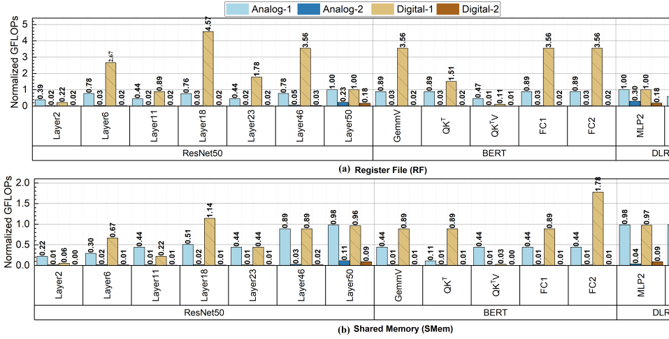
V-C Results on performance
Fig. 7(a) and Fig. 7(c) compare the performance observed when CiM is integrated at RF and SMem level respectively.
What: Comparing different CiM primitives, Analog-1 with the least compute latency (9 cycles) shows performance ranging from 22% to 100% of baseline throughput. On the other hand, Digital-1 (18 cycle compute latency) can achieve as high as 450% of baseline throughput and in general achieves close to baseline throughput, except for certain GEMMs (discussed under when). This implies that the ability to exploit full row and column parallelism is more important, in CiM design, for throughput than achieving lowest possible latency. However, latency can not be ignored completely as depicted by the lower performance of Analog-2 and Digital-2 primitives, having high compute latency of 144 and 233 cycles respectively.
When: Compute-bound layers with bigger weight matrix (Layer6, Layer18, Layer46, GemmV, FC1 and FC2) achieve the highest performance with CiM primitives (minimum 78% of baseline when re-purposed at RF level) compared to other GEMM shapes. Few compute-bound GEMMs, specifically Layer2 and QKTV which have smaller value of K, perform sub-optimally across all CiM primitives and achieve only up to 39% and 47% of baseline throughput respectively. This lower performance is attributed to the lower performance from Digital-1, which stems from the mapping constraints on K dimension. CiM architectures have weights () mapped to reduce multiple partial sums across the K dimension, limiting their parallelism for small K. Whereas baseline does not have such constraints and hence, achieves higher performance for such GEMMs. It is also important to note that the maximum performance from CiM primitives does not go beyond baseline for memory-bound layers (Layer50, MLP2, MLP3) because of limited data reuse.
Where: Considering the highest performance across all CiM primitives, the maximum observed throughput at RF level (400%) is significantly greater than that observed at SMem level (170%). This can be attributed to the smaller area of SMem (164KB) compared to 4 instances of RF (256KB) in a single core, which allows for fewer CiM units in the same area, thereby limiting the maximum achievable throughput. An anomaly to such behaviour is the case when the mapper finds a better mapping with higher utilization at SMem instead of RF due to difference in memory width and height constraints. e.g. MLP3 performs 50% better at SMem with Analog-1 than at RF in spite of having bandwidth throttling when computing at SMem level.
V-D Results on energy consumption
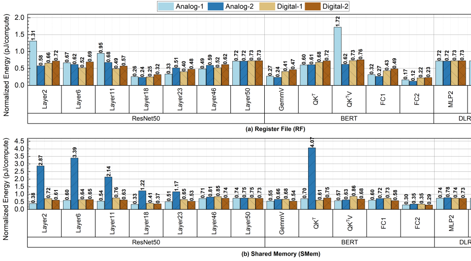
Based on the energy consumption as depicted in Fig. 8(b) and Fig. 8(d), we can make the following observations:
What: There is no clear winner among CiM primitives when it comes to energy efficiency. While the Analog-1 and Analog-2 show the best energy benefits with as low 0.16x and 0.12x of baseline energy for FC2 layer respectively, they also shoot upto 1.7x and 4x of baseline energy for QKTV and QKT layer respectively. On the other hand, Digital-1 and Digital-2 primitives always show reduction in energy consumption ranging from 0.22x-0.86x and 0.23x-0.75x of baseline energy respectively. This suggests that the primitive with the highest TOPS/W (Analog-1 in this case) may not necessarily be the most energy-efficient when main memory is taken into perspective. Nonetheless, CiM primitives can always achieve higher energy efficiency than baseline for all GEMM shapes. For the cases when the primitive is not able to map all the weights (either high or high ) depending on the primitive type and memory level, the total energy consumption becomes larger than baseline due to increase in the number of temporal reductions of the output values. As an example, Analog-2 performs poorly for large , particularly at SMem, because the design parallelizes N dimension and limits K to 64. The effect is pronounced when weight matrix is small (e.g. QKTV for Analog-2-SMem where ) because baseline can efficiently reduce the partial sums and does not require as many accesses to main memory level. Digital-2 at SMem also has fewer CiM units but allows mapping K dimension to different columns in the same array, unlike its analog counterparts.
When: We observed the highest reduction in energy for Layer18, Layer23, GemmV, FC1 and FC2, with upto 0.24x, 0.33x, 0.24x, 0.27x and 0.12x of baseline energy, particularly when re-purposed at RF level. All of these layers have high K value, which explains that the energy benefits from CiM primitives are maximised when there are high number of partial sum reductions. For memory-bound layers (Layer50, MLP2 and MLP3), all CiM primitives exhibit similar benefits with 30% reduction in energy, because the total energy is dominated by DRAM accesses.
Where: RF has more number of CiM units than SMem due to larger area and more instances, which generally leads to lower memory accesses or energy consumption. e.g. Analog-2 benefits the most from computing at RF compared to SMem for QKT layer. The total energy consumption is reduced from 4x to 0.6x of baseline energy with CiM added to SMem and RF respectively. Similarly, Analog-1, Digital-1 and Digital-2 energy consumption is approximately 0.5x, 0.6x and 0.8x at RF as compared to SMem for GemmV, FC1 and FC2 layers respectively. However, on an average across different GEMM shapes, one CiM primitive maybe more suitable for a given memory level depending on the primitive design and GEMM shape. For example, Analog-2 primitive, one with high area overhead, always consumes lower energy when integrated at RF than SMem. For other primitives, energy consumption at SMem could be lower than that at RF, such as that for Layer2 (MNK). Another example is Digital-2 achieving higher energy efficiency on average at SMem as compared to RF.
| Category | Key observation | Reason |
|---|---|---|
| Impact of CiM macro | Maximum throughput gain is achieved by Digital-1 compared to baseline for certain GEMM shapes, across all CiM primitives and memory levels. | The ability to exploit full row and column parallelism helps in increasing the throughput more than compute latency. |
| Analog-2 achieves maximum energy reduction (or highest energy efficiency) with respect to baseline, in spite of Analog-1 being most energy efficient. | Better mapping could compensate for small energy efficiency differences. In this case, mapping of Analog-1 limits the parallelism across K dimension, whereas the mapping of Analog-2 limits the parallelism across N dimension. | |
| Impact of Workload | CiM integrated caches do not increase the performance of memory bound layers. | The throughput of memory bound layers is limited by the main memory bandwidth. |
| GEMMs with high value such as Layer18, Layer23, GemmV, FC1 and FC2 have the highest energy and performance benefits from CiM integration. In contrast, small GEMMs (Layer2 and QKTV) achieve better throughput with baseline than CiM primitives. | CiM primitives inherently perform reduction across K dimensions. This reduces the number of memory accesses for partial sum reductions, but limits the parallelism across dimension. | |
| Impact of Memory Level | Highest performance gains are observed at RF level as compared to SMem level. | Bigger memory capacity allows for more parallelism and can compensate for small data access costs from other cache levels. |
| On an average, Digital-1 achieves better energy efficiency than Digital-2 at RF level whereas Digital-2 gains better energy efficiency than Digital-1 at SMem level. | One CiM primitive may be more suitable for a given memory level depending on their mapping constraints. Digital-2 primitive reserves some bit cells for output values which helps in efficient in-array reduction. This capability becomes more useful when CiM is integrated at memory closer to main memory, by reducing the last level accesses. |
V-E Discussion and Future Work
Takeaways: As the ML models become larger and memory hierarchy evolves, the absolute numbers for performance and energy efficiency gain might change. However, we expect the takeaways (Table VI) to remain the same with iso-area constraints. The takeaways are dependent on the analytical evaluations, considering that 1) performance benefits are decided by the compute latency and compute parallelism, and 2) energy benefits depend on memory accesses and compute cost. For CiM primitives, parallelism, in turn, is decided by the mapping constraints of the CiM primitive, memory capacity, and area overhead. For example, Digital-1 CiM primitive has approximately same area overhead as Analog-1, and almost double the compute latency. Still, Digital-1 achieves higher parallelism due to more flexible mapping constraints which allow full row/column parallelism. On the other hand, energy benefits of CiM depend on the reduction in number of memory accesses and the inherently more energy efficient CiM units. Dataflow plays an important role in reducing the memory accesses and, hence, maximizing CiM benefits, which is taken into account in the analysis.
Assumptions: Our evaluations are based on analytical modelling used in Timeloop and assumes a simplified architecture with fully pipelined memory subsystem. The latency of one memory level access is hidden by the other memory level access in such an architecture if there is no bandwidth throttling. Bandwidth throttling depends on the total number of memory accesses and bandwidth at that memory level. It assumes all accesses are coalesced and does not consider effects such as bank conflicts, limited miss handling buffer capacity, and other architectural optimizations in memory. It still captures the approximate performance of different CiM primitives and helps in gaining an understanding of their impact at system level.
There can be several ways of integrating CiM to the memory subsystem. Integrating CiM at iso-capacity could provide higher parallelism but comes at the cost of increased area. Integrating CiM at iso-memory-area constraints affects the cache memory capacity. This could further affect the baseline throughput of an SM. However, our work envisions an architecture with heterogeneous cores having both CiM and non-CiM SMs in the system architecture. Such an architecture would have similar baseline SM performance.
Additionally, we assumed weight stationary dataflow for all scenarios, as it is the most commonly used dataflow. Adding more flexibility in CiM dataflow could lead to a bigger design space and remains an open search space to explore. Further, recent works [44, 45] have demonstrated floating point CiM accelerators, expanding the scope of computation in memory. However, all experiments in this work assumed INT-8 precision including that in baseline to make it inclusive of a variety of CiM primitives. Further, we only evaluate individual GEMM operations present in ML workloads to estimate the maximum possible performance and energy efficiency gains. For end-to-end analysis, one approach could be to extend Timeloop to include features such as layer-fusion, and non-GEMM operations cost overhead. Inter-layer evaluations also require Timeloop to consider where the inputs, weights and outputs from previous layer reside in the memory hierarchy, which is not supported in the current version. Note, that CiM integrated architectures would also incur a programming cost overhead that should be considered when finalizing the design. Our work provides early-stage estimations for developing such CiM integrated architecture designs.
Future Possibilities: To overcome the area and latency bottleneck from ADC blocks that affect compute parallelism in Analog primitives, Analog ADCless primitives can be considered [46]. Analog ADCless primitives only employ sense amplifiers as peripheral circuits to convert the partial sum from array to a 1bit output. Such low area overhead primitive would results in higher number of CIM units in the same memory area. This would further help in achieving higher performance from higher parallelism, with massive improvements in energy consumption. One caveat with analog primitives is the loss in accuracy of computation. An ADC-less design could lead to large accuracy loss due to aggressive hardware quantization. However, studies[47] suggest that it is possible to achieve minimal accuracy degradation with quantization-aware training techniques.
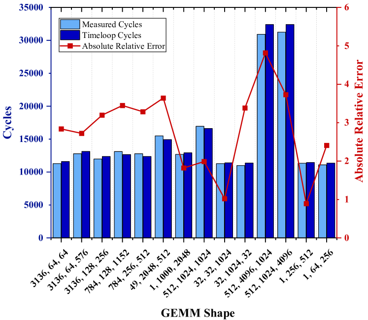
Another way of integrating CiM in a memory subsystem could be to include additional memory levels or change memory technology to include emerging devices. Such studies are outside of scope of this work. However, our methodology can be extended for such analysis and new CiM primitives. The analysis can also be extended to more than one SM architecture to include inter-SM communication or network costs. The complete A100-like GPU model will have 108 SMs and can be used to map bigger models. The performance correlation of our full model version of GPU in Timeloop with specifications from Table V are shown in Fig. 9, where the measured GEMM kernels are run on A100-80GB using CUTLASS 3.2 [48]. However, the design space explodes with full GPU model and increases the dataflow search time manifold. Evaluating full GPU-like model would require optimizations or new methodologies to efficiently find the best mapping in such a large design space.
VI Conclusion
We integrated Compute-in-Memory (CiM) in on-chip cache memory of a GPU architecture. Our experiments provide comprehensive analysis of CIM benefits for accelerating general matrix multiplication (GEMM) workloads, based on Machine Learning (ML) inference tasks, on such a system. Particularly, the iso-area based analytical evaluations lead to the following conclusions:
Regarding what, Digital-1 CiM primitive achieves higher performance (GFLOPs) than baseline for most GEMM shapes because of full row/column parallelism and low area overhead. In contrast, although analog primitives do not reach the high performance levels of Digital-1, they excel in energy efficiency, consuming as little as 0.12x of the baseline energy. Digital primitives follow closely, with best energy savings at 0.22x of baseline. Such trade-offs in energy efficiency and performance with CiM could benefit GPUs, particularly when they operate at a reduced frequency to manage power [49].
The investigation for when indicates that compute-bound layers with high data reuse and large () values benefit the most from CiM in both performance and energy efficiency. For example, fully connected (FC1, FC2) layers in BERT model. Conversely, compute-bound GEMMs with low data reuse and smaller () usually achieve higher throughput with baseline, but show energy advantages with CiM. The initial layers of ResNet50 with Imagenet dataset such as Layer2 and Layer11 in our analysis constitute for such results. Similarly, skewed GEMMs
exhibit energy reduction and comparable throughput for scenarios, but performance declines when . Memory-bound GEMMs such as the fully connected layers in ResNet50 and DLRM only demonstrate energy benefits with CiM, with no improvement in throughput.
Furthermore, the findings for where suggest that capacity of memory is more important than the level number in the memory hierarchy when integrating CiM. Higher memory capacity could lead to higher performance with weight duplication. Energy benefits are also slightly more with higher memory capacity by reducing the number of memory accesses. However, CiM characteristics such as mapping constraints and compute latency could still limit the performance and energy benefits with high memory capacity.
In summary, this work performs a comprehensive evaluation of the trade-offs between energy, area, and performance for CiM primitives across the on-chip memory hierarchy. We believe our work provides key insights in understanding the potential of SRAM based CIM to alleviate the energy problem while achieving comparable performance. In turn, our approach facilitates the optimization of CiM-based architectures for ML inference.
Acknowledgments
The authors would like to acknowledge North America Qualcomn Innovation Fellowship offered in 2021 for funding the project and inputs from Ramesh Chauhan in the initial stage of the project. Part of the research was also funded by CoCoSys, one of the 7 JUMP centers funded by DARPA and SRC. The authors would also like to thank Aayush Ankit for the brainstorming and discussion sessions.
References
- [1] Angshuman Parashar, Priyanka Raina, Yakun Sophia Shao, Yu-Hsin Chen, Victor A Ying, Anurag Mukkara, Rangharajan Venkatesan, Brucek Khailany, Stephen W Keckler, and Joel Emer. Timeloop: A systematic approach to dnn accelerator evaluation. In 2019 IEEE international symposium on performance analysis of systems and software (ISPASS), pages 304–315. IEEE, 2019.
- [2] Yannan N. Wu, Joel S. Emer, and Vivienne Sze. Accelergy: An Architecture-Level Energy Estimation Methodology for Accelerator Designs. In IEEE/ACM International Conference On Computer Aided Design (ICCAD), 2019.
- [3] Jeffrey Welser, Jed W Pitera, and Cindy Goldberg. Future computing hardware for ai. In 2018 IEEE International Electron Devices Meeting (IEDM), pages 1–3. IEEE, 2018.
- [4] Sehoon Kim, Coleman Hooper, Thanakul Wattanawong, Minwoo Kang, Ruohan Yan, Hasan Genc, Grace Dinh, Qijing Huang, Kurt Keutzer, Michael W Mahoney, et al. Full stack optimization of transformer inference: a survey. arXiv preprint arXiv:2302.14017, 2023.
- [5] Wm A Wulf and Sally A McKee. Hitting the memory wall: Implications of the obvious. ACM SIGARCH computer architecture news, 23(1):20–24, 1995.
- [6] Naveen Verma, Hongyang Jia, Hossein Valavi, Yinqi Tang, Murat Ozatay, Lung-Yen Chen, Bonan Zhang, and Peter Deaville. In-memory computing: Advances and prospects. IEEE Solid-State Circuits Magazine, 11(3):43–55, 2019.
- [7] Indranil Chakraborty, Mustafa Ali, Aayush Ankit, Shubham Jain, Sourjya Roy, Shrihari Sridharan, Amogh Agrawal, Anand Raghunathan, and Kaushik Roy. Resistive crossbars as approximate hardware building blocks for machine learning: Opportunities and challenges. Proceedings of the IEEE, 108(12):2276–2310, 2020.
- [8] Jae-Sun Seo. Advances and trends on on-chip compute-in-memory macros and accelerators. In 2023 60th ACM/IEEE Design Automation Conference (DAC), pages 1–6. IEEE, 2023.
- [9] Onur Mutlu, Saugata Ghose, Juan Gómez-Luna, and Rachata Ausavarungnirun. A modern primer on processing in memory. In Emerging Computing: From Devices to Systems: Looking Beyond Moore and Von Neumann, pages 171–243. Springer, 2022.
- [10] Myeonggu Kang, Hyeonuk Kim, Hyein Shin, Jaehyeong Sim, Kyeonghan Kim, and Lee-Sup Kim. S-flash: A nand flash-based deep neural network accelerator exploiting bit-level sparsity. IEEE Transactions on Computers, 71(6):1291–1304, 2022.
- [11] Daichi Fujiki, Scott Mahlke, and Reetuparna Das. Duality cache for data parallel acceleration. In Proceedings of the 46th International Symposium on Computer Architecture, pages 397–410, 2019.
- [12] Daichi Fujiki, Alireza Khadem, Scott Mahlke, and Reetuparna Das. Multi-layer in-memory processing. In 2022 55th IEEE/ACM International Symposium on Microarchitecture (MICRO), pages 920–936. IEEE, 2022.
- [13] Elliot Lockerman, Axel Feldmann, Mohammad Bakhshalipour, Alexandru Stanescu, Shashwat Gupta, Daniel Sanchez, and Nathan Beckmann. Livia: Data-centric computing throughout the memory hierarchy. In ASPLOS, pages 417–433, 2020.
- [14] NVIDIA. Ampere Architecture. https://developer.nvidia.com/blog/nvidia-ampere-architecture-in-depth.
- [15] Jingcheng Wang, Xiaowei Wang, Charles Eckert, Arun Subramaniyan, Reetuparna Das, David Blaauw, and Dennis Sylvester. A 28-nm compute sram with bit-serial logic/arithmetic operations for programmable in-memory vector computing. IEEE Journal of Solid-State Circuits, 55(1):76–86, 2020.
- [16] Xin Si and et al. A local computing cell and 6t sram-based computing-in-memory macro with 8-b mac operation for edge ai chips. IEEE Journal of Solid-State Circuits, 56(9):2817–2831, 2021.
- [17] Mustafa Ali, Indranil Chakraborty, Sakshi Choudhary, Muya Chang, Dong Eun Kim, Arijit Raychowdhury, and Kaushik Roy. A 65 nm 1.4-6.7 tops/w adaptive-snr sparsity-aware cim core with load balancing support for dl workloads. In 2023 IEEE Custom Integrated Circuits Conference (CICC), pages 1–2, 2023.
- [18] Yu-Der Chih et al. 16.4 an 89tops/w and 16.3tops/mm2 all-digital sram-based full-precision compute-in memory macro in 22nm for machine-learning edge applications. In 2021 IEEE International Solid- State Circuits Conference (ISSCC), volume 64, pages 252–254, 2021.
- [19] Haruki Mori et al. A 4nm 6163-tops/w/b sram based digital-computing-in-memory macro supporting bit-width flexibility and simultaneous mac and weight update. In 2023 IEEE International Solid- State Circuits Conference (ISSCC), pages 132–134, 2023.
- [20] Ping-Chun Wu et al. A 28nm 1mb time-domain computing-in-memory 6t-sram macro with a 6.6ns latency, 1241gops and 37.01tops/w for 8b-mac operations for edge-ai devices. In 2022 IEEE International Solid- State Circuits Conference (ISSCC), volume 65, pages 1–3, 2022.
- [21] Hidehiro Fujiwara et al. A 5-nm 254-tops/w 221-tops/mm2 fully-digital computing-in-memory macro supporting wide-range dynamic-voltage-frequency scaling and simultaneous mac and write operations. In 2022 IEEE International Solid- State Circuits Conference (ISSCC), volume 65, pages 1–3, 2022.
- [22] Sharan Chetlur, Cliff Woolley, Philippe Vandermersch, Jonathan Cohen, John Tran, Bryan Catanzaro, and Evan Shelhamer. cudnn: Efficient primitives for deep learning. arXiv preprint arXiv:1410.0759, 2014.
- [23] Nvidia Docs. Matrix Multiplication Background User’s Guide. https://docs.nvidia.com/deeplearning/performance/dl-performance-matrix-multiplication/index.html, 2020-23.
- [24] Samuel Williams, Andrew Waterman, and David Patterson. Roofline: an insightful visual performance model for multicore architectures. Communications of the ACM, 52(4):65–76, 2009.
- [25] Alexandar Devic, Siddhartha Balakrishna Rai, Anand Sivasubramaniam, Ameen Akel, Sean Eilert, and Justin Eno. To pim or not for emerging general purpose processing in ddr memory systems. In Proceedings of the 49th Annual International Symposium on Computer Architecture, pages 231–244, 2022.
- [26] Pouya Houshmand, Jiacong Sun, and Marian Verhelst. Benchmarking and modeling of analog and digital sram in-memory computing architectures. arXiv preprint arXiv:2305.18335, 2023.
- [27] Maxim Naumov, Dheevatsa Mudigere, Hao-Jun Michael Shi, Jianyu Huang, Narayanan Sundaraman, Jongsoo Park, Xiaodong Wang, Udit Gupta, Carole-Jean Wu, Alisson G Azzolini, et al. Deep learning recommendation model for personalization and recommendation systems. arXiv preprint arXiv:1906.00091, 2019.
- [28] Mark Horowitz. 1.1 computing’s energy problem (and what we can do about it). In 2014 IEEE international solid-state circuits conference digest of technical papers (ISSCC), pages 10–14. IEEE, 2014.
- [29] Naresh R Shanbhag and Saion K Roy. Benchmarking in-memory computing architectures. IEEE Open Journal of the Solid-State Circuits Society, 2:288–300, 2022.
- [30] Amogh Agrawal, Mustafa Ali, Minsuk Koo, Nitin Rathi, Akhilesh Jaiswal, and Kaushik Roy. Impulse: A 65-nm digital compute-in-memory macro with fused weights and membrane potential for spike-based sequential learning tasks. IEEE Solid-State Circuits Letters, 4:137–140, 2021.
- [31] Aayush Ankit, Izzat El Hajj, Sai Rahul Chalamalasetti, Geoffrey Ndu, Martin Foltin, R Stanley Williams, Paolo Faraboschi, Wen-mei W Hwu, John Paul Strachan, and Kaushik Roy. Puma: A programmable ultra-efficient memristor-based accelerator for machine learning inference. In ASPLOS, 2019.
- [32] Qing Dong, Mahmut E. Sinangil, Burak Erbagci, Dar Sun, Win-San Khwa, Hung-Jen Liao, Yih Wang, and Jonathan Chang. 15.3 a 351tops/w and 372.4gops compute-in-memory sram macro in 7nm finfet cmos for machine-learning applications. In 2020 IEEE International Solid-State Circuits Conference - (ISSCC), pages 242–244, 2020.
- [33] Angshuman Parashar, Minsoo Rhu, Anurag Mukkara, Antonio Puglielli, Rangharajan Venkatesan, Brucek Khailany, Joel Emer, Stephen W Keckler, and William J Dally. Scnn: An accelerator for compressed-sparse convolutional neural networks. ACM SIGARCH computer architecture news, 45(2):27–40, 2017.
- [34] Hyoukjun Kwon, Prasanth Chatarasi, Vivek Sarkar, Tushar Krishna, Michael Pellauer, and Angshuman Parashar. Maestro: A data-centric approach to understand reuse, performance, and hardware cost of dnn mappings. IEEE micro, 40(3):20–29, 2020.
- [35] Linyan Mei, Pouya Houshmand, Vikram Jain, Sebastian Giraldo, and Marian Verhelst. Zigzag: A memory-centric rapid dnn accelerator design space exploration framework. arXiv preprint arXiv:2007.11360, 2020.
- [36] Yannan Nellie Wu, Vivienne Sze, and Joel S. Emer. Accelergy-Timeloop Processing-in-memory (PIM) Example. https://github.com/Accelergy-Project/processing-in-memory-design, 2020.
- [37] Aaron Stillmaker and Bevan Baas. Scaling equations for the accurate prediction of cmos device performance from 180 nm to 7 nm. Integration, 58:74–81, 2017.
- [38] Kaiming He, Xiangyu Zhang, Shaoqing Ren, and Jian Sun. Deep residual learning for image recognition. corr abs/1512.03385 (2015), 2015.
- [39] Jia Deng, Wei Dong, Richard Socher, Li-Jia Li, Kai Li, and Li Fei-Fei. Imagenet: A large-scale hierarchical image database. In 2009 IEEE conference on computer vision and pattern recognition, pages 248–255. Ieee, 2009.
- [40] Jacob Devlin, Ming-Wei Chang, Kenton Lee, and Kristina Toutanova. Bert: Pre-training of deep bidirectional transformers for language understanding. arXiv preprint arXiv:1810.04805, 2018.
- [41] Markus Nagel, Mart van Baalen, Tijmen Blankevoort, and Max Welling. Data-free quantization through weight equalization and bias correction. In Proceedings of the IEEE/CVF International Conference on Computer Vision, pages 1325–1334, 2019.
- [42] Tim Dettmers, Mike Lewis, Younes Belkada, and Luke Zettlemoyer. Llm. int8 (): 8-bit matrix multiplication for transformers at scale. arXiv preprint arXiv:2208.07339, 2022.
- [43] Tim Rogers and Mahmoud Khairy. Machine Learning Accelerator War. https://www.sigarch.org/an-academics-attempt-to-clear-the-fog-of-the-machine-learning-accelerator-war/.
- [44] Ping-Chun Wu, Jian-Wei Su, Li-Yang Hong, Jin-Sheng Ren, Chih-Han Chien, Ho-Yu Chen, Chao-En Ke, Hsu-Ming Hsiao, Sih-Han Li, Shyh-Shyuan Sheu, et al. A 22nm 832kb hybrid-domain floating-point sram in-memory-compute macro with 16.2-70.2 tflops/w for high-accuracy ai-edge devices. In 2023 IEEE International Solid-State Circuits Conference (ISSCC), pages 126–128. IEEE, 2023.
- [45] Jinshan Yue, Chaojie He, Zi Wang, Zhaori Cong, Yifan He, Mufeng Zhou, Wenyu Sun, Xueqing Li, Chunmeng Dou, Feng Zhang, et al. A 28nm 16.9-300tops/w computing-in-memory processor supporting floating-point nn inference/training with intensive-cim sparse-digital architecture. In 2023 IEEE International Solid-State Circuits Conference (ISSCC), pages 1–3. IEEE, 2023.
- [46] Bonan Yan et al. A 1.041-mb/mm2 27.38-tops/w signed-int8 dynamic-logic-based adc-less sram compute-in-memory macro in 28nm with reconfigurable bitwise operation for ai and embedded applications. In 2022 IEEE International Solid- State Circuits Conference (ISSCC), volume 65, pages 188–190, 2022.
- [47] Utkarsh Saxena, Indranil Chakraborty, and Kaushik Roy. Towards adc-less compute-in-memory accelerators for energy efficient deep learning. In 2022 Design, Automation & Test in Europe Conference & Exhibition (DATE), pages 624–627. IEEE, 2022.
- [48] Vijay Thakkar, Pradeep Ramani, Cris Cecka, Aniket Shivam, Honghao Lu, Ethan Yan, Jack Kosaian, Mark Hoemmen, Haicheng Wu, Andrew Kerr, Matt Nicely, Duane Merrill, Dustyn Blasig, Fengqi Qiao, Piotr Majcher, Paul Springer, Markus Hohnerbach, Jin Wang, and Manish Gupta. CUTLASS. https://github.com/NVIDIA/cutlass, 2023.
- [49] Vijay Kandiah, Scott Peverelle, Mahmoud Khairy, Junrui Pan, Amogh Manjunath, Timothy G Rogers, Tor M Aamodt, and Nikos Hardavellas. Accelwattch: A power modeling framework for modern gpus. In MICRO-54: 54th Annual IEEE/ACM International Symposium on Microarchitecture, pages 738–753, 2021.
VII Biography Section
![[Uncaptioned image]](/html/2312.15896/assets/tanvi.jpg) |
Tanvi Sharma received her bachelor’s degree from Indian Institute of Technology, Roorkee in 2018 and worked as a Digital Design Engineer at Texas Instruments before joining Purdue University in 2019. She is in the direct PhD program at Purdue, under the guidance of Professor Kaushik Roy. She has been a recipient of Qualcomn Innovation Fellowship in 2021, and MLSys Rising Stars Award in 2023. Her research interests lie at the intersection of machine learning and systems, with focus on developing energy efficient ML hardware accelerators using compute-in-memory solutions. |
![[Uncaptioned image]](/html/2312.15896/assets/mustafa_ali.jpg) |
Mustafa Ali received his B.Sc. ans M.Sc. degrees in Electrical Engineering from MTC, Cairo, Egypt in 2011, 2016 respectively. He worked on flexible electronics applications using TFTs in his M.Sc from 2014 to 2016. Additionally, he worked as a TA and RA at MTC from 2013 to 2017. Mustafa was also a hardware and embedded systems engineer at Integreight, Inc. from 2012 to 2017. He joined the Nano-electronics Research Lab (NRL), Purdue University in Spring 2018 to Fall 2022 pursuing his Ph.D. under the guidance of Prof. Roy. His research interest lied in innovative HW accelerating of ML workloads inculding compute in memory. He is currently a hardware engineer at Microsoft Azure Hardware Systems and Infrastructure. |
![[Uncaptioned image]](/html/2312.15896/assets/indranil.jpeg) |
Indranil Chakraborty is currently a Hardware Engineer at Google, Sunnyvale, California. He received the B.Engg. degree in Electronics and Telecommunication Engineering from Jadavpur University, Kolkata, India, in 2013, an M.Tech. degree in Electrical Engineering from Indian Institute of Technology Bombay, Mumbai, India, in 2016 and Ph.D. degree in 2021 at Nanoelectronics Research Laboratory, Purdue University, West Lafayette, IN, USA. His primary research interests lie in architecture and design of hardware accelerators for machine-learning workloads using CMOS and emerging technologies. |
![[Uncaptioned image]](/html/2312.15896/assets/kaushik.png) |
Kaushik Roy is the Edward G. Tiedemann, Jr., Distinguished Professor of Electrical and Computer Engineering at Purdue University. He received his BTech from Indian Institute of Technology, Kharagpur, PhD from University of Illinois at Urbana-Champaign in 1990 and joined the Semiconductor Process and Design Center of Texas Instruments, Dallas, where he worked for three years on FPGA architecture development and low-power circuit design. His current research focuses on cognitive algorithms, circuits and architecture for energy-efficient neuromorphic computing/ machine learning, and neuro-mimetic devices. Kaushik has supervised 100 PhD dissertations and his students are well placed in universities and industry. He is the co-author of two books on Low Power CMOS VLSI Design (John Wiley & McGraw Hill). |