Switching dynamics in Al/InAs nanowire-based gate-controlled superconducting transistor
Abstract
The observation of the gate-controlled supercurrent (GCS) effect in superconducting nanostructures increased the hopes for realizing a superconducting equivalent of semiconductor field-effect transistors. However, recent works attribute this effect to various leakage-based scenarios, giving rise to a debate on its origin. A proper understanding of the microscopic process underlying the GCS effect and the relevant time scales would be beneficial to evaluate the possible applications. In this work, we observed gate-induced two-level fluctuations between the superconducting state and normal state in Al/InAs nanowires (NWs). Noise correlation measurements show a strong correlation with leakage current fluctuations. The time-domain measurements show that these fluctuations have Poissonian statistics. Our detailed analysis of the leakage current measurements reveals that it is consistent with the stress-induced leakage current (SILC), in which inelastic tunneling with phonon generation is the predominant transport mechanism. Our findings shed light on the microscopic origin of the GCS effect and give deeper insight into the switching dynamics of the superconducting NW under the influence of the strong gate voltage.
I Introduction
In 2018, De Simoni et al. De Simoni et al. (2018) observed a monotonic suppression of the supercurrent in titanium (Ti) NWs by increasing the voltage beyond a certain threshold at a nearby gate (side or back) electrode. With further increases in the gate voltage, the supercurrent is fully suppressed, and the device is switched to the normal state, providing a superconducting equivalent of semiconductor CMOS transistors with an expected high switching speed and low power consumption. Moreover, the structure of gate-controlled superconducting nanodevices can be readily scaled up with greater compatibility for interfacing with CMOS transistors in comparison to alternative superconducting devices Buck (1956); Matisoo (1966); Likharev and Semenov (1991); McCaughan and Berggren (2014). The earlier experimental observations of the GCS were associated with various unique fingerprints, which were attributed to the influence of the external -field De Simoni et al. (2018, 2019); Paolucci et al. (2019); Rocci et al. (2020); Puglia et al. (2020); Bours et al. (2020); Mercaldo et al. (2020); Solinas et al. (2021); Mercaldo et al. (2021); Chirolli et al. (2021); Amoretti et al. (2022); Chakraborty et al. (2023). Later on, most of these fingerprints were observed in other works suggesting leakage current-based scenarios Alegria et al. (2021); Ritter et al. (2021); Golokolenov et al. (2021); Elalaily et al. (2021); Ritter et al. (2022); Elalaily et al. (2023); Basset et al. (2021). Furthermore, the different experimental conditions, e.g., superconducting material, substrate, and device configuration, make it hard to compare different works Ruf et al. (2023a, b). As a result, the microscopic origin of the GCS remains controversial. In particular, the role of the leakage current is the key point in the ongoing debate between different studies. Therefore, it will be necessary to understand the microscopic origin behind the GCS effect to assess the reliability of the GCS-based devices to compete with semiconductor technology in various applications.
The low-frequency noise is widely observed in various nanoelectronic devices Balandin (2013); Paladino et al. (2014); Balogh et al. (2021); Falci et al. (2024). Investigation of noise can provide valuable information and a deeper understanding of the transport mechanisms and the dominant sources of fluctuations in different nanodevices Balandin (2013); Paladino et al. (2014); Balogh et al. (2021); Falci et al. (2024). In addition, noise correlation measurements are very powerful techniques that can be used for probing the cross-correlation between different fluctuating quantities in such systems, which has proven to be successful, for example in the investigation of the bosonic or fermionic, or even the anyonic nature of charge carriers in two-dimensional electron gas Büttiker (1992); Liu et al. (1998); Henny et al. (1999); Bartolomei et al. (2020). In this work, we address the GCS effect in Al/InAs NWs with noise measurements for the first time. By carrying out cross-correlation measurements, we show that gate-induced fluctuations in the superconducting NW are directly related to time-dependent leakage current. Furthermore, we performed time-domain measurements to explore the statistics of these fluctuations and the relevant time scales. Finally, based on the detailed analysis of our results, we give a plausible explanation for the microscopic process behind the GCS in the Al/InAs gate-controlled superconducting transistors.
II Experiments
II.1 Device outline and gate influence
We have investigated the GCS in Al/InAs NW-based devices with the device configuration shown in the false-colored SEM image in Fig. 1a (see Methods for the fabrication details). Four Ti/Al contacts (blue) were deposited on top of Al/InAs NW (green) for quasi-four probe measurements. Two Ti/Au side gates (yellow) are placed on opposite sides of the NW and used for tuning the supercurrent in the NW.

We first investigated the GCS effect by measuring the characteristics of the device as a function of in both positive and negative gate polarities, as shown in Fig. 1b, which is similar to earlier observations Elalaily et al. (2021, 2023). As the bias current is swept from negative to positive polarity, there are two borderlines separating the superconducting state (white region) from the normal state regions (blue and red regions). These lower and upper borderlines represent the gate dependence of the retrapping current and the switching current , respectively. At V, the device switches to the normal state at A, while it switches from the normal state to the superconducting state at A. As increases in either positive or negative gate polarity, is suppressed from a certain threshold gate voltage V until it is fully quenched at the critical gate voltage, V. At the gate voltages, where is suppressed, a corresponding enhancement in the leakage current, is observed (see Fig. 1c), similar to what was reported in Refs. 18; 20; 21; 22; 23. Fig. 1d shows selected curves at different gate voltages for the positive polarity of the bias current and gate voltage and separated vertically for clarity. The curve at V (blue curve) shows a well-developed zero resistance below , while at higher gate voltages, e.g., at V (green curve), finite voltage fluctuations across the NW are observed slightly below at the bias current values in the interval of [2,4] A.
Fig. 1e shows the curve measured at V with different current ramp speeds, . At A/s, the curve exhibits noisy region below A. As is increased up to 293 A/s, the NW device becomes less sensitive to these fluctuations, suggesting that the time scale of the fluctuations is the same order of magnitude as the time scale corresponding to the current ramping rate. It also implies that increasing gate voltage does not only suppresses , but also induces a dissipative region in which the voltage across the superconducting NW has dynamical fluctuations.
II.2 Noise correlation measurements
Considering the ongoing debate regarding the origin of the GCS effect, it is valuable to investigate the correlation between gate-induced voltage fluctuations in the superconducting NW and the leakage current, both of which are simultaneously monitored in our experimental setup (see schematic of the measurement setup in Fig. 1a and details in Methods). To investigate this, we first studied the low-frequency fluctuations in the leakage current by measuring the power spectral density of the current noise on the resistor as a function of the applied gate voltage (see the Supporting Information).
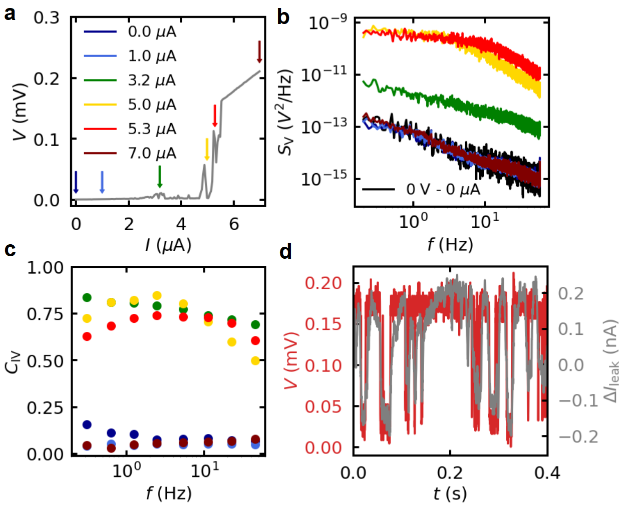
To investigate the gate-induced voltage fluctuations in the NW device, we fixed at 5 V and measured simultaneously the spectral density of the leakage current noise and the induced voltage noise across the NW device as a function of the bias current (see the Supporting Information for complete measurements). Fig. 2a shows the curve of the NW device measured in parallel with the noise measurements. The colored arrows point to working points along the curve where the behavior of the measured noise spectra of the NW device will be studied. These points are representative samples from the three characteristic regimes in which the curve exhibits a pure superconducting state (dark and light blue arrows), voltage fluctuations below (green, red, and yellow arrows), and a pure normal state (brown arrow) with corresponding noise spectra of shown in Fig. 2b. The noise spectra measured in the pure superconducting (dark and light blue curves) have the same amplitude as the background noise originating from the setup (black curve) measured at = 0 A and = 0 V. Similarly, the noise spectrum measured in the normal state (brown curve) also has the same noise level within our experimental resolution. On the other hand, the noise spectra measured in the voltage fluctuation region are more than an order of magnitude larger. Interestingly, the noise spectrum measured at A (green curve) has dependence (), while the spectra at higher bias current values (red and yellow curves) have a steeper slope at higher frequencies () resembling a Lorentzian spectrum (see the Supporting Information).
The cross-correlation between the leakage current noise and the induced noise in the NW was investigated in terms of the coherence (see Methods). If two signals are fully correlated, coherence has a value of 1, while for uncorrelated signals, it is 0. Fig. 2c shows the coherence (averaged per frequency octave) between the two noise signals at different bias current values. The coherence measurements show that it has high values (0.50.8) for the green, yellow, and red curves, corresponding to the entire current region where the voltage fluctuation is observed, while it is for the curves measured at the superconducting and normal states (see the complete measurements in the Supporting Information). This indicates that the voltage fluctuations observed in the superconducting wire are not independent, but they are strongly correlated with the current fluctuation of the leakage between the gate and the superconducting NW. This strong correlation was also confirmed by the time-domain measurements. Fig. 2d shows the time-domain measurements for the fluctuations on the top of the average leakage current (grey curve) and the induced voltage fluctuations in the NW (red curve) at V and at A. The time traces show that the leakage current fluctuates from a low to a high current state, whereas the voltage across the device changes from a zero-voltage state to a finite-voltage state. This strong correlation is a very robust effect as we have observed a high coherence between the leakage current noise and the induced voltage noise across the superconducting NW in three other devices (see the Supporting Information), which confirms the reproducibility of our results.
II.3 Time-domain measurements
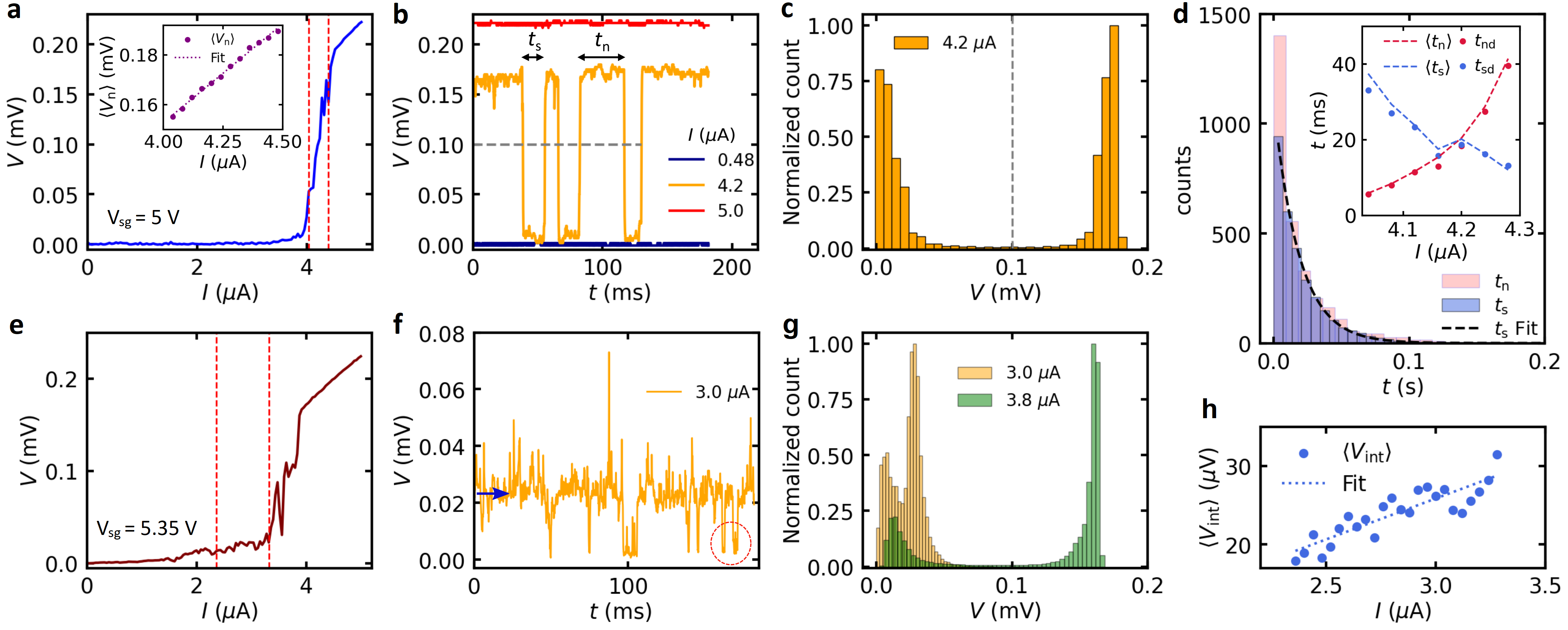
To understand the nature of the induced voltage fluctuations in the NW, we measured the voltage across the superconducting NW as a function of time at a finite gate voltage and different bias current values. Fig. 3a shows the time average curve measured at V. The curve is obtained by averaging a 119 s-long time trace for each bias current value. The time traces were measured by an ultra-high frequency lock-in amplifier (See Methods) with a sampling rate of 27.5 kS/s. Fig. 3b shows typical time traces of at different bias current values in which the device exhibits a pure superconducting state (blue trace measured at 0.48 A), a pure normal state (red trace measured at 5 A), and the regime below (orange trace measured at 4.2 A), where the large voltage fluctuations have been observed. As expected, the time traces measured in the superconducting and normal states show a constant zero-voltage and finite-voltage across the device with time, respectively. On the other hand, the time trace measured in the voltage fluctuation regime shows that the device has voltage fluctuations between two well-defined values, as already seen in Fig. 2d. Figure 3c presents the distribution of the measured voltages constructed from the time traces and normalized by the maximum bin counts at A. It shows a histogram with two peaks, one with a high probability at 0 V, which we identify as the superconducting state. To understand the nature of the high voltage state, we set a threshold at mV, as indicated by the gray dashed line between the two voltage states (see Fig. 2b,c). The voltage above the threshold was averaged for the whole period, denoted by . This average voltage was extracted for different bias currents in the region marked by the red dashed lines in Fig. 3a and plotted as a function of the corresponding bias current (see inset of Fig. 3a). The average voltage increases linearly with the bias current with a corresponding resistance of which is in the same order of magnitude as the normal state resistance measured at A (). This indicates that the high voltage state is the dissipative normal state, and the NW in the voltage fluctuation region oscillates between the superconducting and normal states. This is possible since, at = 5 V, the voltage fluctuations appear slightly below (see the Supporting Information), therefore, it is expected that if the device switches to the normal state, it will be retrapped to the superconducting state.
As the next step to analyze the dynamics of the induced fluctuations in the NW, we extracted the lifetimes and in which the NW is in the superconducting and normal state, respectively. This was implemented by extracting the periods at which the voltage across the device is above and below the threshold at 0.1 V (see Fig. 3b). Fig. 3d shows the distribution of the current-dependent lifetimes (blue color) and (red color) at V and A. The black-dashed curve in Fig. 3d is the fitting of the histogram (blue histogram) with an exponential, with as fitting parameter. The fitting shows that the distribution follows an exponential dependence (See also the Supporting Information). The same fitting was implemented for both distributions, for the bias current values in the interval indicated by the red dashed lines in Fig. 3a. The inset of Fig. 3d presents the extracted decay times and (blue and red circles) and the average lifetimes (blue and red curves) for both distributions as a function of the bias current. The nice matching between the two quantities for both lifetimes indicates that the switching of the NW under the influence of the gate in this region resembles the Poisson process Da Silva et al. (2011). Furthermore, as the bias current is increased, the lifetime of the NW in the normal state is increased, while it stays for a shorter time in the superconducting state. On the other hand, the distribution of the lifetimes indicates that the gate-induced fluctuations in the NW are slow and can have long time scales.
The analysis of the time-domain measurements for the voltage across the NW at = 5 V shows well-defined two-level fluctuations between the superconducting and normal states. However, at higher gate voltages, we noticed that the fluctuations of the system were different. Fig. 3e presents the time-average curve measured at V. Even though the ramp rate of the bias current is very slow (0.336 nA/s), we observed that the time-average of the voltage has almost a constant value where the bias current was increased from A up to A (the bias current interval indicated by the two red dashed lines in Fig. 3e) compared to the same interval in the curve measured at V shown in Fig. 3a. The time trace of the voltage at A is plotted in Fig. 3f, which shows that the system fluctuates between the superconducting state (red circle) and a wide range of different finite voltage values (blue arrow). This can also be observed from the normalized distribution (yellow distribution) of these voltage states shown in Fig. 3g. Since the finite-voltage state is not at the same level as the normal-state voltage, we will denote it as the intermediate-voltage state. Fig. 3h shows the average voltage of the intermediate state as a function of the bias current in the interval indicated by the two red dashed lines in Fig. 3e. The resistance obtained from fitting the curve with a linear function is . which is significantly lower than that of the normal state. As the bias current increases beyond this regime, e.g., at A, the distribution (green distribution in Fig. 3g) shows that the system fluctuates between a low-voltage state and the normal state (see also the Supporting Information). These fluctuations resemble those observed at V, i.e., Fig. 3c (having a resistance of 80 ).
III Discussion
In order to understand the origin of the noise in the leakage current, we should emphasize that the gate dependence of the device has been investigated in two different cooldowns. In the first cooldown, the switching current of the NW device was fully suppressed at 15 V applied on the gate (see the Supporting Information) after initial training measurements Elalaily et al. (2021). In the second cooldown, this gate voltage window where is fully suppressed has been reduced to 6 V (see Fig. 1b) after initial training. Fig. 4a shows the as a function of in both cooldowns. The enhancement of the leakage current at lower gate voltages in both cooldowns after increasing the applied gate voltage to a high value is consistent with the stress-induced leakage current (SILC) that was observed in thin gate oxides of the MOSFET transistors Maserjian and Zamani (1982); Chou et al. (1997); Alers et al. (1998).
As discussed in Ref. 36, as the gate oxide is stressed under a high electric field in the Fowler-Nordheim regime (see Fig. 4c), the high-energy electrons tunneling through the oxide potential barrier suffer collisions with the atoms of the oxide, resulting in damage and hence creating charge traps in the oxide layer. These charge traps serve as intermediate tunneling sites, which can increase the leakage current at lower applied voltages via trap-assisted tunneling. In the case of thick oxides, as in our case (the oxide layer between the gate and the NW), multiple traps are assumed to assist in the conduction process Schuler et al. (2002); Ielmini et al. (2002). The generated charge traps can trap electrons and randomly release them with long time constants giving rise to fluctuations in the trap-assisted tunneling and hence the presence of noise in the Ralls et al. (1984); Alers et al. (1998). These time scales are consistent with the time scales of fluctuations observed in our case (see Fig. 3d). Since originates from the tunneling of the electrons from one electrode to the other through the trap states, the trapping and detrapping of the electrons by the charge traps change the transmission probability through the oxide and result in resistance fluctuations. For this mechanism, the normalized current noise should be independent of the applied gate voltages Alers et al. (1998). Fig. 4b shows the as a function of at Hz in the gate voltage window at which is suppressed. The ratio is constant with increasing , which is consistent with the fluctuation of the charge traps generated in the oxide layer after the initial training period Alers et al. (1998). Furthermore, the dominant conduction mechanism in the SILC is inelastic tunneling Takagi et al. (1999), in which electron energy relaxation is usually associated with the emission of phonons (see Fig. 4d) Sakakibara et al. (1997); Jiménez-Molinos et al. (2001). In our case, the emitted phonons can propagate through the substrate, couple with the superconducting NW, and cause the GCS effect Ritter et al. (2022). In addition, this energy relaxation could also excite surface plasmons, and their decay with photon generation can also contribute to GCS Lambe and McCarthy (1976).
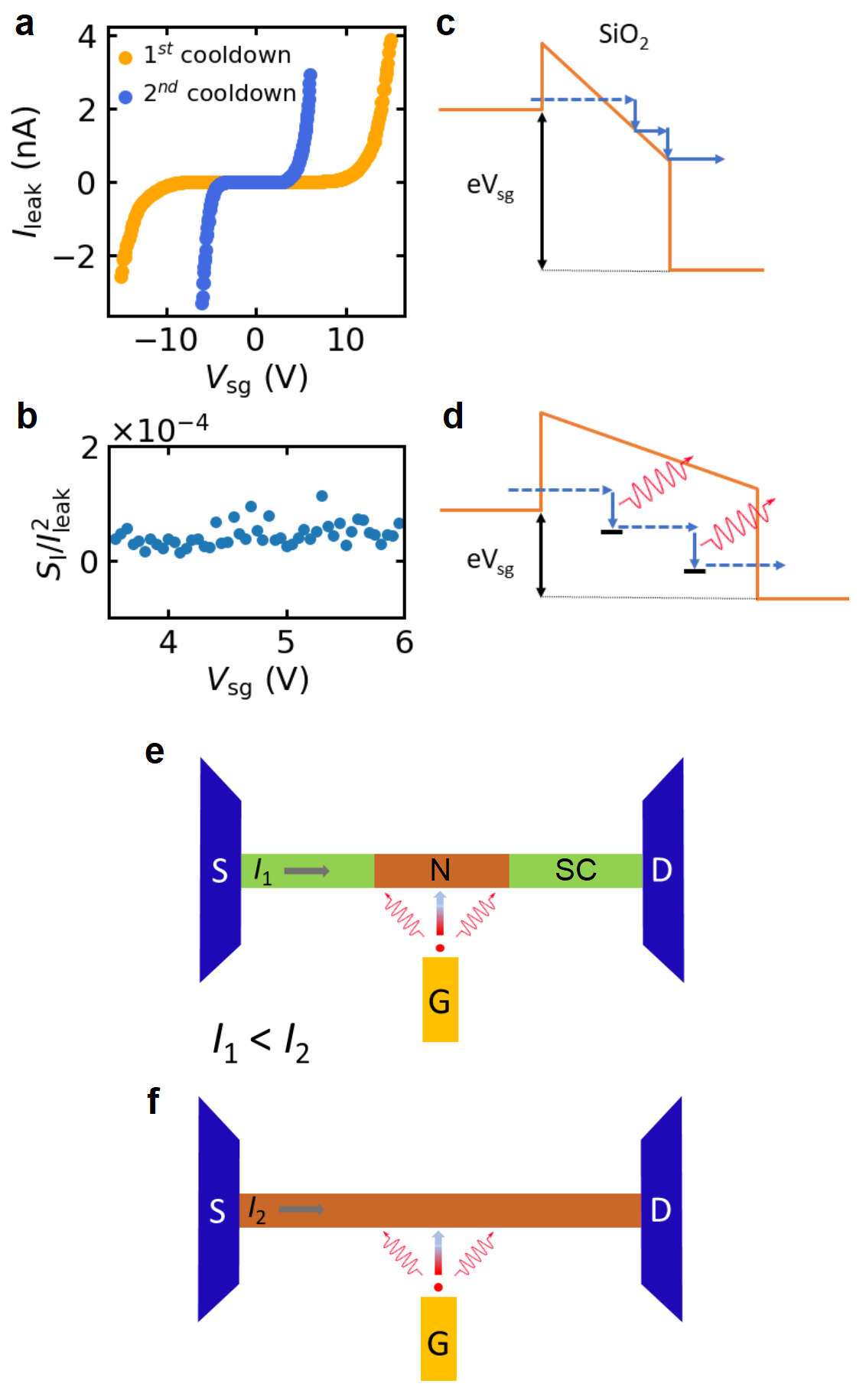
Considering the time-domain measurements at 5.35 V, the appearance of an intermediate-voltage state (see Fig. 3f) with a resistance of at lower bias current values is consistent with a short segment of the NW having been switched to the normal state (see Fig. 4e). As is increased, the leakage current fluctuations become stronger and more frequent. This can induce phase slips in the superconducting NW at the position where more energy is transferred (see orange region) Shah et al. (2008); Bezryadin (2013). Since the bias current is small, the heat dissipated by the phase slip is not enough to switch the whole superconducting NW to its normal state. The ratio indicates that the NW segment that switched to the normal state has a length of nm, which is consistent with the minimal size of a phase slip center, which has a value of nm (see Methods) Tinkham (2004), where is the coherence length in the Al shell. The scattering in the value of (see Fig. 3f) can be attributed to the wide energy distribution of the generated phonons Ritter et al. (2022); Basset et al. (2021); Elalaily et al. (2023), which results in fluctuations in the size of the normal segment. Another possibility is that the system exhibits rapid transitions between the superconducting and normal states, which cannot be resolved by the measurement setup. In this case, the entire NW switches to the normal state, and the intermediate-voltage value is determined by the time spent in the normal and superconducting states.
As the bias current is increased, the leakage current fluctuations drive the two-level fluctuation of the superconducting NW (see Fig. 2d). This is because the heat dissipated by the induced phase slips becomes sufficient to switch the whole NW to the normal state (see Fig. 4f). Since and are almost equal at this gate voltage, the device will be retrapped again to the superconducting state when the fluctuating leakage current gets reduced. As the system fluctuates between two discrete voltage states, the power spectral density of the NW noise will have a Lorentzian spectrum (see Fig. 2b). With further increasing the bias current, the heat dissipated by the phase slips will be enough to switch the device and keep it in its normal state. The measurements at two different gate voltages are consistent with this picture since at lower gate voltages (e.g., at ), the induced voltage fluctuations appear at larger bias current values, where the Joule heating switches the whole NW to the normal state and it retraps back to the superconducting state. At large gate voltages (e.g., at ), the gate-induced fluctuations are increased such that they can induce voltage fluctuations already at low bias current values, but this is only enough to switch a short segment of the NW to the normal state, while at larger bias current values the NW fluctuates between the entire superconducting and normal states as discussed before.
IV Conclusions and outlooks
We characterized the GCS effect in Al/InAs NW-based devices by noise measurements. The noise correlation measurements show a large correlation between the leakage current noise and the induced voltage noise in the superconducting NW. Our findings suggest that the GCS effect originated from phonons generated by inelastic tunneling of the electrons through the trap states created by stressing the oxide layer between the gate and the NW under a high electric field, which is qualitatively consistent with the microscopic picture proposed by Ref. Ritter et al. (2022).
Moreover, our results show that even an individual resistance fluctuator can control the switching of the supercurrent in the nanowire. This is an important finding, which means that even a very small change in the inelastic tunneling current at a critical spot can lead to abrupt switching of the supercurrent. Identification of such a critical spot would make these systems very promising elements for fast superconducting electronics. These spots are likely in close contact with the nanowire, where the influence of the generated phonons is maximized. Furthermore, besides phonon emission in inelastic tunneling, there should also be photon emission, which could also contribute to the switching of the superconductor. Such photons could be directly verified using low-temperature optical emission experiments.
Considering superconducting gating for fast logic circuits, the speed of switching back to the superconducting state is expected to be the limiting factor since it is governed by thermal processes and their intrinsic speed. With Al superconductor below 1 K the thermal response speeds are limited to frequencies GHz owing to low superconducting transition temperature. However, by using materials with large critical temperatures such as NbTiN Machhadani et al. (2019), much larger thermal speeds could be achieved. Presuming that the operation temperature can be increased from to 5 K, electronic thermal cooling will be replaced by electron-phonon heat transfer Gershenzon et al. (1990), and the operation speed can be increased by two orders of magnitude, which is suitable for the implementation of fast logic gates. Furthermore, the GCS effect can be useful in various quantum circuits as a fast gate tunable superconducting-normal switch. This could find application e.g., in SQUID-based CPR measurements Della Rocca et al. (2007) to switch off the reference junction, or such a unit can be used as a heat switch as well.
Methods
The devices were fabricated by depositing InAs NWs with a 20 nm-thick full Al shell layer (green) Krogstrup et al. (2015) on an undoped Si wafer with a 290 nm-thick oxide layer. After NWs deposition, four Ti/Al contacts (blue) with a thickness of 10/80 nm and two opposite side gates (yellow) made of Ti/Au with a thickness of 7/33 nm were fabricated in two separate electron beam lithography (EBL) steps. For the device shown in Fig. 1a, the separation between the Al contacts is nm. The distance between the upper gate electrode and the NW is nm, while for the lower gate electrode, it is nm. All the GCS-based measurements on this particular device were performed by applying a voltage to the upper gate electrode.
The characteristics of the device were measured using a quasi-4-probe method in which the current is ramped linearly from negative to positive values by an engineered voltage signal generated by an arbitrary wave function generator (KEYSIGHT 33600A) with a series resistor of 50 k, while the voltage across the device is measured with a differential low-noise voltage amplifier and a Zürich instruments (UHF-LI 600 MHz) used as an oscilloscope. The ramping rate of the bias current can be controlled by adjusting the sampling frequency of the waveform generator.
The leakage current noise and the voltage noise in the NW device were probed by measuring the noise signals at the gate resistor and the NW device, respectively. The noise signals were measured by a 2-channel spectrum analyzer (HP89410A). The obtained noise spectra were averaged 20 times. The cross-spectrum and the coherence between the two signals were calculated internally by the spectrum analyzer.
The high-resolution time traces for the voltage fluctuations in the NW device were measured by the quasi-4-probe measurements, whereas the bias current is kept fixed and the voltage across the device is measured as a function of time by the Zürich instruments. On the other hand, the time traces in which both the two signals (leakage current and NW fluctuations) were measured simultaneously were probed by a multi-channel oscilloscope (Tektronix TDS 2014B).
The coherence between two signals and is defined at a given frequency as follows: Carter (1987)
| (1) |
where,
| (2) |
is the cross-spectrum between the two signals, is the time delay between the two signals, denotes the the expectation value. and are the corresponding power spectral densities of the two signals. takes values between 0 and 1, and if the value of the coherence is close to 1, the two signals are strongly correlated. Conversely, the two signals are uncorrelated if the value of the coherence is close to 0 Carter (1987).
The coherence length was calculated by using De Simoni et al. (2018), where nm, nm and nm are the length, width, and thickness of the NW device, respectively, is the density of states at Fermi level, and , = 1 K.
Author contributions
T.E. and M.B. fabricated the devices, T.E., I.L., and A.S. performed the measurements T.E., M.B., G.F., and L. K. did the data analysis. T.K. and J.N. developed the nanowires. All authors discussed the results and worked on the manuscript. P.M., P.H., and S.C. guided the project.
Acknowledgments
This work was funded by the EU’s Horizon 2020 research and innovation program under grant Supergate (964398), COST Action CA 21144 superqumap, ERC Twistrain, the FET Open AndQC grant (828948), OTKA K138433 and EIC Pathfinder Challenge QuKiT (101115315), and by the Doctoral Excellence Fellowship Programme (DCEP) of NRDIF, BME and NKFIH, the grant TKP2021-NVA-02 of NKFIH and VEKOP 2.3.3-15-2017-00015. The work was also supported by Quantum Information National Laboratory of Hungary (Grant No. 2022-2.1.1-NL-2022-00004), the Academy of Finland projects 341913 (EFT), and 312295 & 352926 (CoE, Quantum Technology Finland). The research leading to these results has received funding from the European Union’s Horizon 2020 Research and Innovation Programme, under Grant Agreement no 824109 (EMP). This research made use of the OtaNano – Low-Temperature Laboratory infrastructure of Aalto University. This research was supported by the Carlsberg Foundation, and the Danish National Research Foundation (DNRF 101).
References
- De Simoni et al. (2018) G. De Simoni, F. Paolucci, P. Solinas, E. Strambini, and F. Giazotto, “Metallic supercurrent field-effect transistor,” Nature nanotechnology 13, 802–805 (2018).
- Buck (1956) D. A. Buck, “The cryotron-a superconductive computer component,” Proceedings of the IRE 44, 482–493 (1956).
- Matisoo (1966) J. Matisoo, “Subnanosecond pair-tunneling to single-particle tunneling transitions in josephson junctions,” Applied Physics Letters 9, 167–168 (1966).
- Likharev and Semenov (1991) K. K. Likharev and V. K. Semenov, “Rsfq logic/memory family: A new josephson-junction technology for sub-terahertz-clock-frequency digital systems,” IEEE Transactions on Applied Superconductivity 1, 3–28 (1991).
- McCaughan and Berggren (2014) A. N. McCaughan and K. K. Berggren, “A superconducting-nanowire three-terminal electrothermal device,” Nano letters 14, 5748–5753 (2014).
- De Simoni et al. (2019) G. De Simoni, F. Paolucci, C. Puglia, and F. Giazotto, “Josephson field-effect transistors based on all-metallic al/cu/al proximity nanojunctions,” ACS nano 13, 7871–7876 (2019).
- Paolucci et al. (2019) F. Paolucci, G. De Simoni, P. Solinas, E. Strambini, N. Ligato, P. Virtanen, A. Braggio, and F. Giazotto, “Magnetotransport experiments on fully metallic superconducting dayem-bridge field-effect transistors,” Physical Review Applied 11, 024061 (2019).
- Rocci et al. (2020) M. Rocci, G. De Simoni, C. Puglia, D. D. Esposti, E. Strambini, V. Zannier, L. Sorba, and F. Giazotto, “Gate-controlled suspended titanium nanobridge supercurrent transistor,” ACS nano 14, 12621–12628 (2020).
- Puglia et al. (2020) C. Puglia, G. De Simoni, and F. Giazotto, “Electrostatic control of phase slips in ti josephson nanotransistors,” Physical Review Applied 13, 054026 (2020).
- Bours et al. (2020) L. Bours, M. T. Mercaldo, M. Cuoco, E. Strambini, and F. Giazotto, “Unveiling mechanisms of electric field effects on superconductors by a magnetic field response,” Physical Review Research 2, 033353 (2020).
- Mercaldo et al. (2020) M. T. Mercaldo, P. Solinas, F. Giazotto, and M. Cuoco, “Electrically tunable superconductivity through surface orbital polarization,” Physical Review Applied 14, 034041 (2020).
- Solinas et al. (2021) P. Solinas, A. Amoretti, and F. Giazotto, “Sauter-schwinger effect in a bardeen-cooper-schrieffer superconductor,” Physical Review Letters 126, 117001 (2021).
- Mercaldo et al. (2021) M. T. Mercaldo, F. Giazotto, and M. Cuoco, “Spectroscopic signatures of gate-controlled superconducting phases,” Physical Review Research 3, 043042 (2021).
- Chirolli et al. (2021) L. Chirolli, T. Cea, and F. Giazotto, “Impact of electrostatic fields in layered crystalline bcs superconductors,” Physical Review Research 3, 023135 (2021).
- Amoretti et al. (2022) A. Amoretti, D. K. Brattan, N. Magnoli, L. Martinoia, I. Matthaiakakis, and P. Solinas, “Destroying superconductivity in thin films with an electric field,” Physical Review Research 4, 033211 (2022).
- Chakraborty et al. (2023) S. Chakraborty, D. Nikolić, J. C. Cuevas, F. Giazotto, A. Di Bernardo, E. Scheer, M. Cuoco, and W. Belzig, “Microscopic theory of supercurrent suppression by gate-controlled surface depairing,” arXiv preprint arXiv:2303.07801 (2023).
- Alegria et al. (2021) L. D. Alegria, C. G. Bøttcher, A. K. Saydjari, A. T. Pierce, S. H. Lee, S. P. Harvey, U. Vool, and A. Yacoby, “High-energy quasiparticle injection into mesoscopic superconductors,” Nature Nanotechnology , 1–5 (2021).
- Ritter et al. (2021) M. Ritter, A. Fuhrer, D. Haxell, S. Hart, P. Gumann, H. Riel, and F. Nichele, “A superconducting switch actuated by injection of high-energy electrons,” Nature communications 12, 1–6 (2021).
- Golokolenov et al. (2021) I. Golokolenov, A. Guthrie, S. Kafanov, Y. A. Pashkin, and V. Tsepelin, “On the origin of the controversial electrostatic field effect in superconductors,” Nature Communications 12, 1–7 (2021).
- Elalaily et al. (2021) T. Elalaily, O. Kürtössy, Z. Scherübl, M. Berke, G. Fülöp, I. E. Lukács, T. Kanne, J. Nygård, K. Watanabe, T. Taniguchi, P. Makk, and S. Csonka, “Gate-controlled supercurrent in epitaxial al/inas nanowires,” Nano letters 21, 9684–9690 (2021).
- Ritter et al. (2022) M. Ritter, N. Crescini, D. Haxell, M. Hinderling, H. Riel, C. Bruder, A. Fuhrer, and F. Nichele, “Out-of-equilibrium phonons in gated superconducting switches,” Nature Electronics 5, 71–77 (2022).
- Elalaily et al. (2023) T. Elalaily, M. Berke, M. Kedves, G. Fülöp, Z. Scherübl, T. Kanne, J. Nygård, P. Makk, and S. Csonka, “Signatures of gate-driven out-of-equilibrium superconductivity in ta/inas nanowires,” ACS nano 17, 5528–5535 (2023).
- Basset et al. (2021) J. Basset, O. Stanisavljević, M. Kuzmanović, J. Gabelli, C. Quay, J. Estève, and M. Aprili, “Gate-assisted phase fluctuations in all-metallic josephson junctions,” Physical Review Research 3, 043169 (2021).
- Ruf et al. (2023a) L. Ruf, T. Elalaily, C. Puglia, Y. P. Ivanov, F. Joint, M. Berke, A. Iorio, P. Makk, G. De Simoni, S. Gasparinetti, G. Divitini, S. Csonka, F. Giazotto, E. Scheer, and A. Di Bernardo, “Effects of fabrication routes and material parameters on the control of superconducting currents by gate voltage,” APL Materials 11, 091113 (2023a).
- Ruf et al. (2023b) L. Ruf, C. Puglia, G. De Simoni, Y. P. Ivanov, T. Elalaily, F. Joint, M. Berke, J. Koch, A. Iorio, S. Khorshidian, A. Makk, Peter Vecchione, S. Gasparinetti, S. Csonka, W. Belzig, M. Cuoco, G. Divitini, F. Giazotto, E. Scheer, and A. Di Bernardo, “Gate-control of superconducting current: relevant parameters and perspectives,” arXiv preprint arXiv:2302.13734 (2023b).
- Balandin (2013) A. A. Balandin, “Low-frequency 1/f noise in graphene devices,” Nature nanotechnology 8, 549–555 (2013).
- Paladino et al. (2014) E. Paladino, Y. Galperin, G. Falci, and B. Altshuler, “1/f noise: Implications for solid-state quantum information,” Reviews of Modern Physics 86, 361 (2014).
- Balogh et al. (2021) Z. Balogh, G. Mezei, L. Pósa, B. Sánta, A. Magyarkuti, and A. Halbritter, “1/f noise spectroscopy and noise tailoring of nanoelectronic devices,” Nano Futures 5, 042002 (2021).
- Falci et al. (2024) G. Falci, P. J. Hakonen, and E. Paladino, “1/f noise in quantum nanoscience,” in Encyclopedia of Condensed Matter Physics (Second Edition), edited by T. Chakraborty (Academic Press, Oxford, 2024) second edition ed., pp. 1003–1017.
- Büttiker (1992) M. Büttiker, “Scattering theory of current and intensity noise correlations in conductors and wave guides,” Physical Review B 46, 12485 (1992).
- Liu et al. (1998) R. Liu, B. Odom, Y. Yamamoto, and S. Tarucha, “Quantum interference in electron collision,” Nature 391, 263–265 (1998).
- Henny et al. (1999) M. Henny, S. Oberholzer, C. Strunk, T. Heinzel, K. Ensslin, M. Holland, and C. Schonenberger, “The fermionic hanbury brown and twiss experiment,” Science 284, 296–298 (1999).
- Bartolomei et al. (2020) H. Bartolomei, M. Kumar, R. Bisognin, A. Marguerite, J.-M. Berroir, E. Bocquillon, B. Placais, A. Cavanna, Q. Dong, U. Gennser, et al., “Fractional statistics in anyon collisions,” Science 368, 173–177 (2020).
- Da Silva et al. (2011) R. Da Silva, L. C. Lamb, and G. I. Wirth, “Collective poisson process with periodic rates: applications in physics from micro-to nanodevices,” Philosophical Transactions of the Royal Society A: Mathematical, Physical and Engineering Sciences 369, 307–321 (2011).
- Maserjian and Zamani (1982) J. Maserjian and N. Zamani, “Behavior of the si/sio2 interface observed by fowler-nordheim tunneling,” Journal of Applied Physics 53, 559–567 (1982).
- Chou et al. (1997) A. I. Chou, K. Lai, K. Kumar, P. Chowdhury, and J. C. Lee, “Modeling of stress-induced leakage current in ultrathin oxides with the trap-assisted tunneling mechanism,” Applied physics letters 70, 3407–3409 (1997).
- Alers et al. (1998) G. Alers, B. Weir, M. Alam, G. Timp, and T. Sorch, “Trap assisted tunneling as a mechanism of degradation and noise in 2-5 nm oxides,” in 1998 IEEE International Reliability Physics Symposium Proceedings. 36th Annual (Cat. No. 98CH36173) (IEEE, 1998) pp. 76–79.
- Schuler et al. (2002) F. Schuler, R. Degraeve, P. Hendrickx, and D. Wellekens, “Physical description of anomalous charge loss in floating gate based nvm’s and identification of its dominant parameter,” in 2002 IEEE International Reliability Physics Symposium. Proceedings. 40th Annual (Cat. No. 02CH37320) (IEEE, 2002) pp. 26–33.
- Ielmini et al. (2002) D. Ielmini, A. S. Spinelli, A. L. Lacaita, and A. Modelli, “Modeling of anomalous silc in flash memories based on tunneling at multiple defects,” Solid-State Electronics 46, 1749–1756 (2002).
- Ralls et al. (1984) K. Ralls, W. Skocpol, L. Jackel, R. Howard, L. Fetter, R. Epworth, and D. Tennant, “Discrete resistance switching in submicrometer silicon inversion layers: Individual interface traps and low-frequency (1 f?) noise,” Physical review letters 52, 228 (1984).
- Takagi et al. (1999) S.-i. Takagi, N. Yasuda, and A. Toriumi, “Experimental evidence of inelastic tunneling in stress-induced leakage current,” IEEE Transactions on Electron Devices 46, 335–341 (1999).
- Sakakibara et al. (1997) K. Sakakibara, N. Ajika, K. Eikyu, K. Ishikawa, and H. Miyoshi, “A quantitative analysis of time-decay reproducible stress-induced leakage current in sio/sub 2/films,” IEEE Transactions on Electron Devices 44, 1002–1008 (1997).
- Jiménez-Molinos et al. (2001) F. Jiménez-Molinos, A. Palma, F. Gámiz, J. Banqueri, and J. López-Villanueva, “Physical model for trap-assisted inelastic tunneling in metal-oxide-semiconductor structures,” Journal of Applied Physics 90, 3396–3404 (2001).
- Lambe and McCarthy (1976) J. Lambe and S. McCarthy, “Light emission from inelastic electron tunneling,” Physical Review Letters 37, 923 (1976).
- Shah et al. (2008) N. Shah, D. Pekker, and P. M. Goldbart, “Inherent stochasticity of superconductor-resistor switching behavior in nanowires,” Physical review letters 101, 207001 (2008).
- Bezryadin (2013) A. Bezryadin, Superconductivity in Nanowires: Fabrication and Quantum Transport (John Wiley & Sons, Weinheim, Germany, 2013).
- Tinkham (2004) M. Tinkham, Introduction to superconductivity (Courier Corporation, 2004).
- Machhadani et al. (2019) H. Machhadani, J. Zichi, C. Bougerol, S. Lequien, J.-L. Thomassin, N. Mollard, A. Mukhtarova, V. Zwiller, J.-M. Gérard, and E. Monroy, “Improvement of the critical temperature of nbtin films on iii-nitride substrates,” Superconductor Science and Technology 32, 035008 (2019).
- Gershenzon et al. (1990) E. Gershenzon, M. Gershenzon, G. Gol’tsman, A. Lyul’kin, A. Semenov, and A. Sergeev, “Electron-phonon interaction in ultrathin nb films,” Sov. Phys. JETP 70, 505–511 (1990).
- Della Rocca et al. (2007) M. Della Rocca, M. Chauvin, B. Huard, H. Pothier, D. Esteve, and C. Urbina, “Measurement of the current-phase relation of superconducting atomic contacts,” Physical review letters 99, 127005 (2007).
- Krogstrup et al. (2015) P. Krogstrup, N. Ziino, W. Chang, S. Albrecht, M. Madsen, E. Johnson, J. Nygård, C. M. Marcus, and T. Jespersen, “Epitaxy of semiconductor–superconductor nanowires,” Nature materials 14, 400–406 (2015).
- Carter (1987) G. C. Carter, “Coherence and time delay estimation,” Proceedings of the IEEE 75, 236–255 (1987).